Unit - 2
Applications of 8051 Microcontroller
In the design of all microprocessor-based system, Semiconductor memory are used as primary storage for code and data. It can be in units of K bits, M bits and so on. Semiconductor memories are conducted directly to the CPU and is also called as primary memory. The widely used semiconductor memories are ROM and RAM.
Characteristics of Semiconductor Memory
Memory capacity- The number of bits that a semiconductor memory chip can store is called chip capacity
Memory organization- Memory chips are organized into number of locations within the IC. Each location holds 1 bit, 4bits, 8bits or even 16 bits, depending on how it is designed internally.
1. A memory chip contains 2x locations where x is the number of address pins.
2. Each location contains y bits, where y is the number of data pins on the chip.
3. The entire chip will contain 2x x y bits, where x is the number of address pins and y is the number of data pins.
Speed- One of the most important characteristics of a memory chip is the speed at which its data can be accessed.
ROM (Read-Only-Memory)- It is a type of memory that does not loss its contents when the power is turned off. For this reason ROM is called volatile memory. There are different types of read-only- memory such as PROM, EPROM, EEPROM, Flash EPROM and mask ROM.
PROM- It refers to the kind of ROM that the user can burn information into it. That’s why it is called as user-programmable memory. For every bit of the PROM, there exists a fuse. So it is programmed by blowing of fuses. It is also referred to as OTP (one –time programmable)
EPROM (Erasable Programmable ROM)- In EPROM, one can program the memory chip and erase it thousands of times. A widely used EPROM is called UV-EPROM. The content of UV-EPROM is erased when it is exposed to ultra violet light. Its erase time is near about 20 minutes.
EEPROM (Electrically Erasable Programmable ROM)- Its desired contents are erased by electrically.
Flash memory EPROM- This memory has become popular user-programmable memory chip, due to the process of erasure of the entire contents takes less than a second. As the erasure method is electrical sometimes it is called as Flash EEPROM.
Mask ROM- Mask ROM refers to kind of ROM in which the contents are programmed by the IC manufacturer. It is not a user-programmable ROM.
RAM (Random Access Memory)- It is called volatile memory since cutting of the power to the IC will result in the loss of data. Sometimes it is called as read and write memory (RAWM). There are three types of RAMs: Static RAM (SRAM), NV-RAM (Non-volatile RAM) and dynamic RAM (DRAM).
NV-RAM (Non-volatile RAM)-This RAM is non-volatile. Like other RAMs it allows the CPU to read write to it, but when the power is turned off, the contents are not lost. To retain its content every NV-RAM chip internally is made of the following components.
1. It uses extremely power-efficient. SRAM cells built out of CMOS
2. It uses an internal lithium battery as back energy source.
3. It uses an intelligent control circuitry. The main job of internal circuitry to monitor the Vcc pin constantly to detect the loss of external power supply. If the power to the Vcc pin falls the below out-of-tolerance condition, the control circuitry switches automatically to its internal power source, lithium battery.
DRAM (Dynamic RAM)-The use of a capacitor as a means to store data cuts down the number of transistors needed to build up the cell; however, it requires constant refreshing due to leakage. This is in contrast to SRAM whose cells are made of flip-lops. The use of capacitor as storage cells in DRAM results in much smaller net memory size.
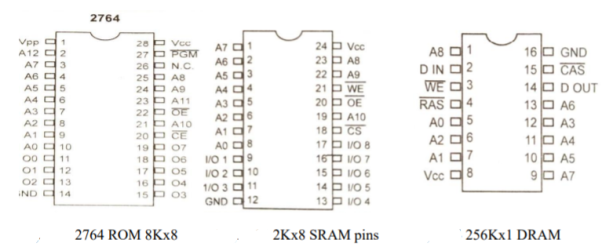
Memory Address Decoding
The job of the decoding circuitry to locate the selected memory block that CPU has access to desired data in memory chip. Memory chips have one more pins called CS (chip select) which must be activated for the memory contents to be accessed. Sometimes the chip select is also referred to as Chip Enable (CE). Following points are required for interfacing the memory to the CPU.
1. The data bus of the CPU is connected directly to data pins of the memory chip.
2. Control signals RD (read) and WR write from the CPU are connected to the OE (output enable) and WE (write enable) pins of memory chips respectively.
3. In case of the address buses, while lower bits of the addresses from the CPU are connected directly to the address pins of the memory chips and upper address pins are used to activate the CS or CE pin of the memory chip. The CS or CE pin along with RD/WR allows the flow of data in or out of the memory chip.

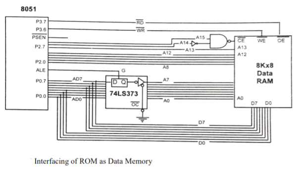
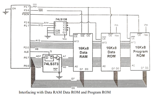
Interfacing with External ROM/RAM as Program and Data Memory
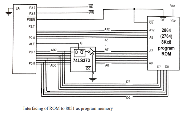
For interfacing to external ROM some pins have important role that to be discussed here. EA-When this pin is connected to Vcc, that indicates the program code is stored in the microcontroller on-chip ROM. For external ROM access tis pin is grounded.
P0 and P2 role in providing addresses- In 8051 P0 and P2 provides the 16-bit address to access external memory. Of these ports P0 provides the lower 8 bit addresses A0-A7, and P2 provides the upper 8 bit addresses A8-A15. More importantly, P0 is also used to provide 8 bit- data bus D0-D7. In other words P0.0- P0.7 are used for both address and Data is called as address/data multiplexing. The sharing of this bus is accomplished by ALE (address latch enable.) Pin. When ALE=0, the 8051 uses P0 for the data path and when ALE=1, it is used for address path.
 (program store enable)- It is an output signal must be connected to OE pin of a ROM containing the program code. When
  pin is connected to ground the 8051 fetches opcode from external ROM by using
  .
.

LCD
To interface LCD with PIC microcontroller use GPIO pins because we need to send control and data signals to LCD through these I/O pins.
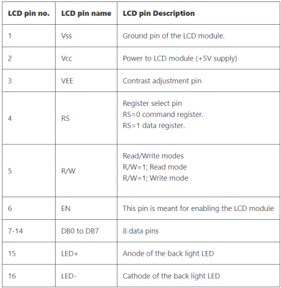

Figure. LCD
In 8-bit mode interfacing, use 11 pins of pic microcontroller and in 4-bit mode use 6 GPIO pins.
A variable resistor is used to adjust the contrast of 5×8 dot pixels according to background light.
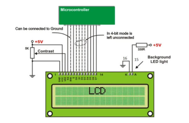
Figure. 4/8 bit mode Interfacing
To interface LCD, follow these steps:
- Define PIC18F4450 pin that we want to use for sending commands and data to LCD
- After that send configuration commands to select mode and other configuration settings
- Once successfully configured LCD, transmit data to LCD.
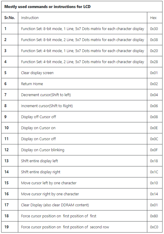
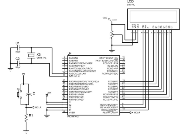
Figure. Interfacing LCD
LED
Light Emitting Diodes are considered as semi- conductor light sources. The commonly used LEDs have a cut-off voltage of 1.7V and current of 10mA. When applied with its required voltage and current it glows with full intensity.
The Light Emitting Diode works similar to normal PN- diode but it emits energy in the form of light. The colour of the light depends on the semiconductors band gap.

Figure. LED
LED is connected to AT89C51 microcontroller with the current limiting resistor. The value of this resistor is calculated using the following formula.
R= (V-1.7)/10mA, where V is the input voltage.
The maximum output voltage of microcontrollers is 5V. Hence the calculated value of resistor is 330 Ohms. The resistor can be connected to cathode or the anode of LED.
- Initially, burn the code into the microcontroller.
- Connect the LEDs to the Port0 of the microcontroller.
- Switch on the circuit.
- The LEDs start glowing.
- Switch off the circuit.
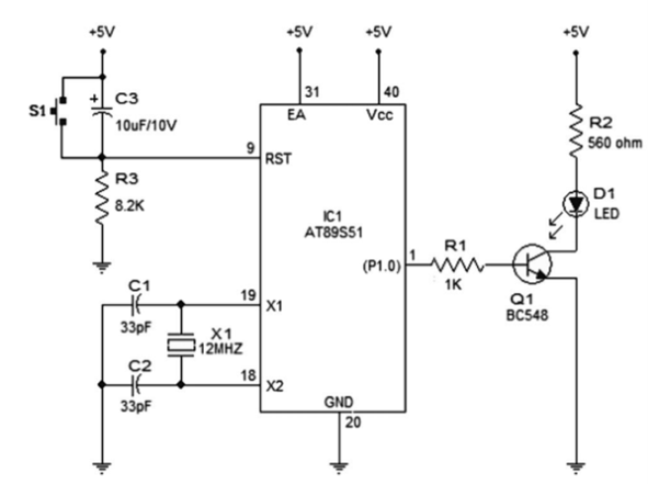
Figure. LED Interfacing
- In the circuit, push button switch S1, capacitor C3 and resistor R3 forms the reset circuitry.
- When S1 is pressed, voltage at the reset pin (pin9) goes high and this resets the chip. C1, C2 and X1 are related to the on -chip oscillator to produces the required clock frequency.
- P1.0 (pin1) is acts as the output pin. When P1.0turns high transistor Q1 is forward biased and LED gets ON. When P1.0 turns low, the transistor gets cut off and the LED extinguishes.
- The transistor driver circuit for the LED can be avoided and the LED can be connected directly to the P1.0 pin along with the series current limiting resistor(~1K).
- The time for which P1.0turns high and low (time period of the LED) is determined by the program.
Program:
START: CPL P1.0
ACALL WAIT
SJMP START
WAIT: MOV R4,#05H
WAIT1: MOV R3,#00H
WAIT2: MOV R2,#00H
WAIT3: DJNZ R2,WAIT3
DJNZ R3,WAIT2
DJNZ R4,WAIT1
RET
Keypad is used as an input device to read the key pressed by user and to process it.
4x4 keypad consists of 4 rows and 4 columns. Switches are placed between the rows and columns. A key press establishes a connection between corresponding row and column between which the switch is placed.
In order to read the key press we need to configure the rows as outputs and columns as inputs.
Columns are read after applying signals to the rows in order to determine whether a key is pressed or not and if pressed, which key is pressed.
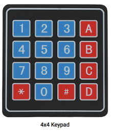
Figure. Keyboard matrix

Figure. Keyboard Interfacing
#include <pic18f4550.h>
#include "Configuration_Header_File.h"
#include "16x2_LCD_4bit_File.h"
Unsigned char keyfind(); /* function to find pressed key */
#define write_port LATB /* latch register to write data on port */
#define read_port PORTB /* PORT register to read data of port */
#define Direction_Port TRISB
Unsigned char col_loc,rowloc,temp_col;
Unsigned char keypad[4][4]= {'7','8','9','/',
'4','5','6','*',
'1','2','3','-',
' ','0','=','+'};
Void main()
{
Char key;
OSCCON = 0x72;
RBPU=0; /* activate pull-up resistor */
LCD_Init(); /* initialize LCD16x2 in 4-bit mode */
LCD_String_xy(0,0,"Press a Key");
LCD_Command(0xC0); /* display pressed key on 2nd line of LCD */
While(1)
{
Key = keyfind(); /* find a pressed key */
LCD_Char(key); /* display pressed key on LCD16x2 */
}
}
Unsigned char keyfind()
{
Direction_Port = 0xf0; /* PORTD.0-PORTD.3 as a Output Port and PORTD.4-PORTD.7 as a Input Port*/
Unsigned char temp1;
Write_port = 0xf0; /* Make lower nibble as low(Gnd) and Higher nibble as High(Vcc) */
Do
{
Do
{
Col_loc = read_port & 0xf0; /* mask port with f0 and copy it to col_loc variable */
}while(col_loc!=0xf0); /* Check initially at the start there is any key pressed*/
Col_loc = read_port & 0xf0; /* mask port with f0 and copy it to col_loc variable */
}while(col_loc!=0xf0);
MSdelay(50);
Write_port = 0xf0; /* Make lower nibble as low(Gnd) and Higher nibble as High(Vcc) */
Do
{ do
{
Col_loc = read_port & 0xf0;
}while(col_loc==0xf0); /* Wait for key press */
Col_loc = read_port & 0xf0;
}while(col_loc==0xf0); /* Wait for key press */
MSdelay(20);
Col_loc = read_port & 0xf0;
While(1)
{
Write_port = 0xfe; /* make Row0(D0) Gnd and keep other row(D1-D3) high */
Col_loc = read_port & 0xf0; /* Read Status of PORT for finding Row */
Temp_col=col_loc;
If(col_loc!=0xf0)
{
Rowloc=0; /* If condition satisfied get Row no. Of key pressed */
While(temp_col!=0xf0) /* Monitor the status of Port and Wait for key to release */
{
Temp_col = read_port & 0xf0; /* Read Status of PORT for checking key release or not */
}
Break;
}
Write_port = 0xfd; /* make Row1(D1) Gnd and keep other row(D0-D2-D3) high */
Col_loc = read_port & 0xf0; /* Read Status of PORT for finding Row */
Temp_col=col_loc;
If(col_loc!=0xf0)
{
Rowloc=1; /* If condition satisfied get Row no. Of key pressed*/
While(temp_col!=0xf0) /* Monitor the status of Port and Wait for key to release */
{
Temp_col = read_port & 0xf0; /* Read Status of PORT for checking key release or not */
}
Break;
}
Write_port = 0xfb; /* make Row0(D2) Gnd and keep other row(D0-D1-D3) high */
Col_loc = read_port & 0xf0; /* Read Status of PORT for finding Row*/
Temp_col=col_loc;
If(col_loc!=0xf0)
{
Rowloc=2; /* If condition satisfied get Row no. Of key pressed */
While(temp_col!=0xf0) /* Wait for key to release */
{
Temp_col = read_port & 0xf0; /* Read Status of PORT for checking key release or not */
}
Break;
}
Write_port = 0xf7; /* make Row0(D3) Gnd and keep other row(D0-D2) high */
Col_loc = read_port & 0xf0; /* Read Status of PORT for finding Row */
Temp_col=col_loc;
If(col_loc!=0xf0)
{
Rowloc=3; /* If condition satisfied get Row no. Of key pressed */
While(temp_col!=0xf0) /* Wait for key to release */
{
Temp_col = read_port & 0xf0; /* Read Status of PORT for checking key release or not */
}
Break;
}
}
While(1)
{
If(col_loc==0xe0)
{
Return keypad[rowloc][0]; /* Return key pressed value to calling function */
}
Else
If(col_loc==0xd0)
{
Return keypad[rowloc][1]; /* Return key pressed value to calling function */
}
Else
If(col_loc==0xb0)
{
Return keypad[rowloc][2]; /* Return key pressed value to calling function */
}
Else
{
Return keypad[rowloc][3]; /* Return key pressed value to calling function */
}
}
MSdelay(300);
}
Stepper motors is mainly used to translate electrical pulses into mechanical movements.
They are used in some disk drives, dot matrix printers. The key advantage of using stepper motor is its position control.
Stepper motors generally have a permanent magnet shaft (rotor), and it is surrounded by a stator.
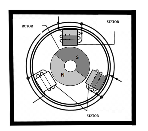
Figure: Stepper Motor
Parameters of stepper motors:
Step Angle - The step angle is the angle at which the rotor moves when one pulse is applied as an input to the stator. This parameter determines the position of stepper motor.
Steps per Revolution - This is the number of step angles required for a complete revolution. The formula is 360° /Step Angle.
Steps per Second - This parameter is used to measure number of steps covered in each second.
RPM - The RPM is the Revolution Per Minute. It measures the frequency of rotation. We can measure the number of rotations in one minute.
The relation between RPM steps per revolution and steps per second is
Steps per second = rpm x steps per revolution / 60
Interfacing
Port P0 of 8051 is used for connecting the stepper motor. HereULN2003 is used. This is basically a high voltage, high current Darlington transistor array. Each ULN2003 has seven NPN Darlington pairs. It can provide high voltage output with common cathode clamp diodes for switching inductive loads.
The Unipolar stepper motor works in three modes.
Wave Drive Mode: In this mode, one coil is energized at a time. So all four coils are energized one after another. This mode produces less torque than full step drive mode.
Steps | Winding A | Winding B | Winding C | Winding D |
1 | 1 | 0 | 0 | 0 |
2 | 0 | 1 | 0 | 0 |
3 | 0 | 0 | 1 | 0 |
4 | 0 | 0 | 0 | 1 |
Full Drive Mode: In this mode, two coils are energized at the same time. This mode produces more torque. Here the power consumption is also high.
Steps | Winding A | Winding B | Winding C | Winding D |
1 | 1 | 1 | 0 | 0 |
2 | 0 | 1 | 1 | 0 |
3 | 0 | 0 | 1 | 1 |
4 | 1 | 0 | 0 | 1 |
Half Drive Mode: In this mode, one and two coils are energized alternately. At first, one coil is energized then two coils are energized. This is basically a combination of wave and full drive mode. It increases the angular rotation of the motor.
Steps | Winding A | Winding B | Winding C | Winding D |
1 | 1 | 0 | 0 | 0 |
2 | 1 | 1 | 0 | 0 |
3 | 0 | 1 | 0 | 0 |
4 | 0 | 1 | 1 | 0 |
5 | 0 | 0 | 1 | 0 |
6 | 0 | 0 | 1 | 1 |
7 | 0 | 0 | 0 | 1 |
8 | 1 | 0 | 0 | 1 |
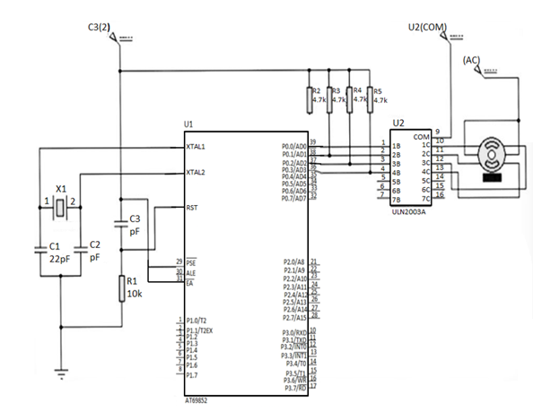
Figure. Interfacing Stepper Motor with 8051
Program:
Main: MOV A, # 0FF H ; Initialization of Port 1
MOV P1, A ;
MOV A, #77 H ; Code for the Phase 1
MOV P1, A ; ACALL DELAY ; Delay subroutine
MOV A, # BB H ; Code for the Phase II
MOV P1, A ;
ACALL DELAY ; Delay subroutine.
MOV A, # DD H ; Code for the Phase III
MOV P1, A ; ACALL DELAY ;
MOV A, # EE H ; Code for the Phase 1
MOV P1, A ;
ACALL DELAY ; Delay subroutine
SJMP MAIN; Keep the motor rotating continuously.
DELAY Subroutine
MOV R4, #0FF H ; Load R4 with FF
MOV R5, # 0FF ; Load R5 with FF
LOOP1: DJNZ R4, LOOP1 ; Decrement R4 until zero,wait
LOOP2: DJNZ R5, LOOP2 ; Decrement R5 until zero,wait
RET ; Return to main program .
DC Motor
DC motor normally works in 6-12v, 300mA and it has other drawbacks like the back EMF produced by the DC motor may harm the controller ports and damage them. The solution to the above problems is using motor driving circuit usually known as H-Bridges. They are basically built using FETs and many dedicated ICs are also available like L293D etc.
These are dual H-bridge motor drivers that is by using one IC we can control two DC motors in both clockwise and counter clockwise directions. The L293D can provide bidirectional drive currents of up to 600mA at voltages from 4.5 V to 36 V.
The below circuit shows interfacing L293D with PIC microcontroller to control a DC motor.

Figure. DC motor circuit
In both ICs, drivers are enabled in pairs with drivers 1 and 2 are enabled by a high input to 1,2 EN and drivers 3 and 4 are enabled by a high input to 3,4 EN. When drivers are enabled, their outputs will be active and in phase with their inputs. When drivers are disabled, their outputs will be off and will be in the high-impedance state.
For example, we use 20MHz clock and the o/p frequency is 2KHz;
Whereas PWM period = 1/frequency (that will be 1/2000 = .0005)
.0005 = [PR2 + 1] • [1 / 20000000] • 16
PR2 + 1 = [.0005 • 20000000] / 16
PR2 + 1 = 625
PR2 = 624
PR2 = 0x270 ( 624 in hex)
Program:
Void main()
{
Short duty = 0; //initial value for duty
TRISD = 0xFF; //PORTD as input
TRISC = 0x00; //PORTC as output
TRISB = 0x00; //PORTB as output
PORTB = 0x02; //Run motor in anticlock wise
PWM1_Init(1000); //Initialize PWM1
PWM1_Start(); //start PWM1
PWM1_Set_Duty(duty); //Set current duty for PWM1
While (1) // endless loop
{
If (!RD0_bit && duty<260) //if button on RD0 pressed
{
Delay_ms(40);
Duty = duty + 10; //increment current_duty
PWM1_Set_Duty(duty); //Change the duty cycle
}
If (!RD1_bit && duty >0) //button on RD1 pressed
{
Delay_ms(40);
Duty = duty - 10; //decrement duty
PWM1_Set_Duty(duty);
}
Delay_ms(10); // slow down change pace a little
}
}
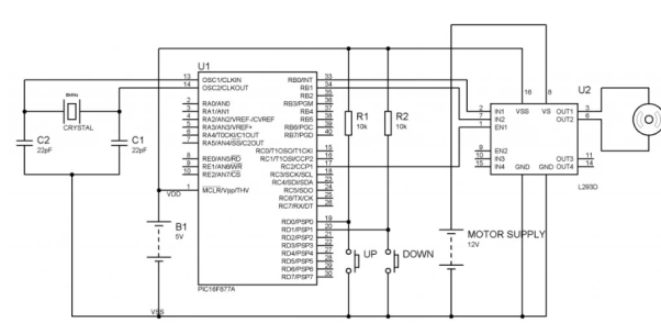
Figure. Interfacing DC motor with PIC
Key takeaway
Stepper motors is mainly used to translate electrical pulses into mechanical movements.
They are used in some disk drives, dot matrix printers. The key advantage of using stepper motor is its position control.
A/D
ADC0808/0809 is a monolithic CMOS device which consists of 28 pin and gives 8-bit value in output for 8- channel ADC input pins (IN0-IN7).
It has resolution of 8 therefore it can encode the analog data into one of the 256 levels (28).
It has three channel address line namely: ADDA, ADDB and ADDC to select channel.
Pin Diagram for ADC0808
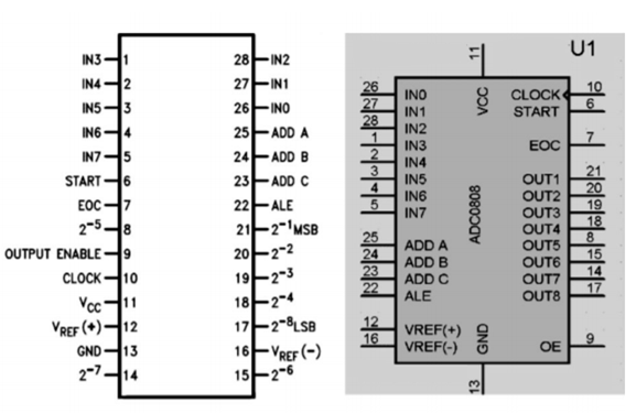
Figure. ADC 0808 Pin
ADC0808/0809 needs clock pulse for conversion which can be provided by using oscillator or microcontroller.
Select the input channel using address lines, like the input line IN0 by keeping all three address lines (ADDA, ADDB,ADDC) low.
Suppose IN2 is selected the keep ADDA and ADDB low and ADDC high.
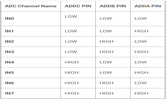
Figure. Channel selection
SOC [Start of conversion]:
When High to low signal is appears on the pin of ADC, and ADC starts conversion

Figure. SOC
EOC [End of conversion]:
To indicate completion of conversion ADC sends high EOC signal to microcontroller.
OE [Output Enable]:
When a high signal is applied to this pin, the output latch of ADC is enabled and the converted data is made available to Microcontroller.
The reference voltage determines the range of analog input voltage.
For example: - If reference voltage is 5V then analog voltage ranges from 0V-5V. If the reference voltage is 2.56V then the range is from 0V-2.56V.
The frequency of the applied clock signal determines conversion speed.
Working:
- Initially, microcontroller provides a 500 KHz clock signal to ADC0808 because the Timer 0 interrupt requires clock signal to operate to operate as ADC.
- Then the microcontroller sends a LOW to HIGH level signal to ALE pin (active-high pin) of ADC0808 to enable the latch in the address.
- By applying HIGH to LOW Level signal to SC (Start Conversion), ADC starts analog to digital conversion. And then wait for the EOC (End of Conversion) pin to go LOW.
- When EOC goes LOW, it means analog to digital conversion has been completed and data is ready to use.
- After this, microcontroller enables the output line by applying a HIGH to LOW signal to OE pin of ADC0808.
- ADC0808 gives ratio metric conversion output at its output pins.
Radiometric conversion is given by
Vin/(Vfs – Vz) = Dx / (Dmax – Dmin)
Where:
Vin is input voltage for conversion
Vfs is full scale voltage
Vz is zero voltage
Dx is data point being measured
Dmax is maximum data limit
Dmin is minimum data limit.
Interfacing Diagram:
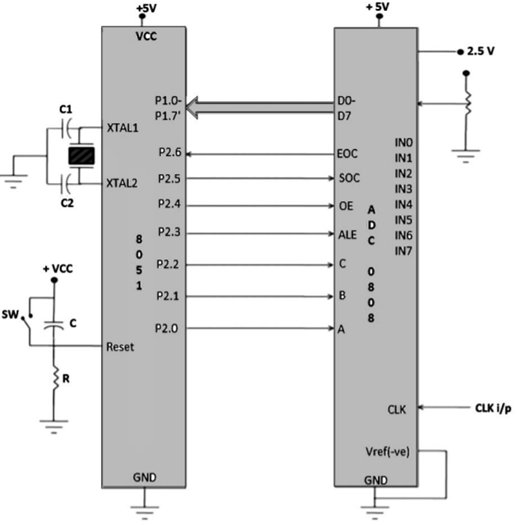
Figure. Interfacing 8051 with ADC0808
Program:
SOC EQU P2.6
EOC EQU P2.5
OE EQU P2.4
ALE EQU P2.3
ADDR_C EQU P2.2
ADDR_B EQU P2.1
ADDR_A EQU P2.0
ORG 0000H
MOV P1, #0FFH
SETB P2.5
CLR SOC
CLR OE
CLR ALE
AGAIN: CLR ADDR_C
CLR ADDR_B
CLR ADDR_A
SETB SOC
SET ALE
ACALL DELAY
CLR SOC
CLR ALE
BACK: JB EOC BACK
HERE: JNB EOC HERE
SETB OE
MOV A,P1
ACALL CONVERSION
ACALL DISPLAY
AGAIN: SJMP AGAIN
Key takeaway
ADC0808/0809 needs clock pulse for conversion which can be provided by using oscillator or microcontroller.
SOC- When High to low signal is appears on the pin of ADC, andADC starts conversion
EOC- To indicate completion of conversion ADC sends high EOC signal to microcontroller.
D/A (0808)
In these systems the microcontroller generates output in digital form, The controlling system requires analog signal because they don't accept digital data. Hence, there is a need to use DAC which converts digital data into its equivalent analog voltage.
In the figure shown, we use 8-bit DAC 0808. This IC converts digital data into its equivalent analog current. The I to V converter converts the current into its equivalent voltage.
According to theory of DAC Equivalent analog output is given as:

Ex:
1. IF data =00H [00000000] and
Vref = 10V

Therefore, V0= 0 Volts.
2. If data is 80H [10000000],
And Vref = 10V

Therefore, V0= 5 Volts.
Different Analog output voltages for different Digital signal is given as:
DATA | OUTPUT VOLTAGE |
00H | 0V |
80H | 5V |
FFH | 10V |
Interfacing Diagram

Figure. Interfacing 8051 with DAC 0808
Program:
ORG 000H
MOV P1, #00H
Call squarwave
Call triwave
Call stairwave
Jmp repeat
Squarwave: MOV P1,#FFH
Call delay2sec
MOV P1,#00H
Call delay2sec
Ret
Triwave: MOV R7,#00H
Triwave1: MOV P1,R7
Inc R7
Cjne R7, #FFH, triwave1
MOV R7, #FFh
Triwave2: MOV P1, R7
Djnz R7, triwave2
RET
Stairwave: MOV P1, #00H
Call delay2sec
MOV P1, #20H
Call delay2sec
MOV P1, #40H
Call delay2sec
RET
Delay1sec: MOV R0,#10
Del2 : MOV R1,#250
Del1: MOV R2,#250
DJNZ R2,$
DJNZ R1,del2
DJNZ R0,del1
RET
Delay2sec: MOV R0,#20
Del2 : MOV R1,#250
Del1: MOV R2,#250
DJNZ R2,$
DJNZ R1,del21
DJNZ R0,del22
RET
END
Key takeaway
In these systems the microcontroller generates output in digital form, The controlling system requires analog signal because they don't accept digital data. Hence, there is a need to use DAC which converts digital data into its equivalent analog voltage.
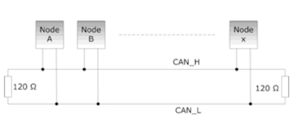
Controller Area Network (CAN) is a serial network technology that was originally designed for the automotive industry, especially for European cars, but has also become a popular bus in industrial automation as well as other applications. The CAN bus is primarily used in embedded systems, and as its name implies, is a network technology that provides fast communication among microcontrollers up to real-time requirements, eliminating the need for the much more expensive and complex technology of a Dual-Ported RAM.
CAN is a two-wire, half duplex, high-speed network system, that is far superior to conventional serial technologies such as RS232 in regards to functionality and reliability and yet CAN implementations are more cost effective.
While, for instance, TCP/IP is designed for the transport of large data amounts, CAN is designed for real-time requirements and with its 1 MBit/sec baud rate can easily beat a 100 MBit/sec TCP/IP connection when it comes to short reaction times, timely error detection, quick error recovery and error repair.
CAN networks can be used as an embedded communication system for microcontrollers as well as an open communication system for intelligent devices. Some users, for example in the field of medical engineering, opted for CAN because they have to meet particularly stringent safety requirements.
Similar requirements had to be considered by manufacturers of other equipment with very high safety or reliability requirements (e.g. Robots, lifts and transportation systems).
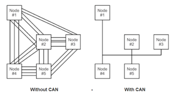
The greatest advantage of Controller Area Network lies in the reduced amount of wiring combined with an ingenious prevention of message collision (meaning no data will be lost during message transmission).
Key takeaway
- Is a serial networking technology for embedded solutions.
- Needs only two wires named CAN_H and CAN_L.
- Operates at data rates of up to 1 Megabit per second.
- Supports a maximum of 8 bytes per message frame.
- Does not support node IDs, only message IDs. One application can support multiple message IDs.
- Supports message priority, i.e. the lower the message ID the higher its priority.
- Supports two message ID lengths, 11-bit (standard) and 29-bit (extended).
- Does not experience message collisions (as they can occur under other serial technologies).
- Is not demanding in terms of cable requirements. Twisted-pair wiring is sufficient.
Bluetooth
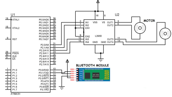
Bluetooth is appropriate. Teri Open wireless protocol for exchanging data over short distances from fixed and mobile devices, creating personal area networks. It was originally convinced as a wireless alternative to RS-232 data cables. Bluetooth is a promising standard for short range wireless communication. Bluetooth uses the same frequency as Wave Lan but with much less effect. But anyhow, some claim that Wave Lan cannot coexist with a fully equipped Bluetooth environment. Bluetooth is a wireless technology for transmission of voice and data over a short distance. R XD and TXD pins on Bluetooth evaluation kit connected with. Controller through serial port.
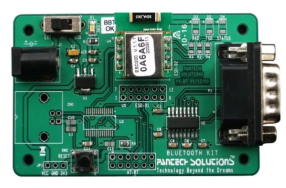
Fig. Bluetooth interface board
USB protocols
Universal serial bus is a set of interface specifications for high speed wired communication between electronics systems peripherals and devices with or without PC/ computer. The USB was originally developed in 1995 by many of the industry leading companies like Intel, Compaq, Microsoft, Digital, IBM and Northern Telecom. The major goal of USB was to define an external expansion bus to add peripherals to a PC in easy and simple manner.
USB offers users simple connectivity. It eliminates the mix of different connectors for different devices like printers, keyboards, mice and other peripherals. That means USB-bus allows many peripherals to be connected using a single standardized interface socket. It supports all kinds of data, from slow mouse inputs to digitized audio and compressed video.
USB also allows hot swapping. The hot-swapping means that devices can be plugged and unplugged without rebooting the computer or turning off the devices. That means, when unplugged in, everything configures automatically. Once the user finished, they can simply unplug the cable out, the host will detect its absence and automatically unload the driver. This makes the USB a plug-and-play interface between a computer and add-on devices.
USB is now the most used interface to connect devices like mouse, keyboards, PDAs, game-pads and joysticks, scanners, scanners, digital cameras, printers, personal media players and flash drives to personal computers. USB sends data in serial mode i.e. the parallel data is serialized before sends and deserialized after receiving.
The benefits of USB are low cost, expandability, auto-configuration, hot- plugging and outstanding performance. It also provides power to the bus, enabling many peripherals to operate without the added need for AC power adapter.
Various version USB
USB1.0: USB 1.0 is the original release of USB having the capability of transferring 12 Mbps, supporting up to 127 devices. The USB 1.0 specification model was introduced in January 1996.
USB1.1: USB 1.1 came out in September 1998. USB 1.1 is known as full speed USB. The version is similar to the original release of USB; however, there are minor modifications for the hardware and the specifications. USB version 1.1 supported two speeds, a full speed mode of 12Mbits/s and a low-speed mode of 1.5 M bits/s.
USB2.0: HP, Intel, LSI corporation, Microsoft, NE, and Philips jointly led the initiative to develop a higher data transfer rate than the 1.1 specifications. The USB 2.0 specifications was released in April 2000 and was standardized at the end of 2001.
Supporting three speed motors (1.5, 12 and 480Mbps), USB 2.0 supports low-bandwidth devices such as keyboards and mice, as well as high-bandwidth ones like high-resolution web-cams, scanners, printers and high-capacity storage systems.
USB 2.0 also known as hi-speed USB. This hi-speed USB is capable of supporting a transfer rate of up to 480 Mbps, compared to 12Mbps of USB 1.1.
USB3.0: USB 3.0 is the latest version of USB release. It is also called as super speed USB having a data transfer rate of 4.8 Gbps (600MB/s). That means it can deliver over 10x the speed of today’s Hi-speed USB connections. The USB 3.0 specifications was released by Intel and its partners in August 2008. Product using the 3.0 specifications are come out in 2010.
The USB tiered star topology
The USB system is made up of a host, multiple numbers of USB ports, and multiple peripheral devices connected in a tiered star topology. The host is the USB systems master and as such controls and schedules all communications activities. Peripherals the devices controlled by USBR slaves responding to commands from the host USB devices are linked in series through hubs. There always exist one hub known as the root hub, which is built into the host controller.
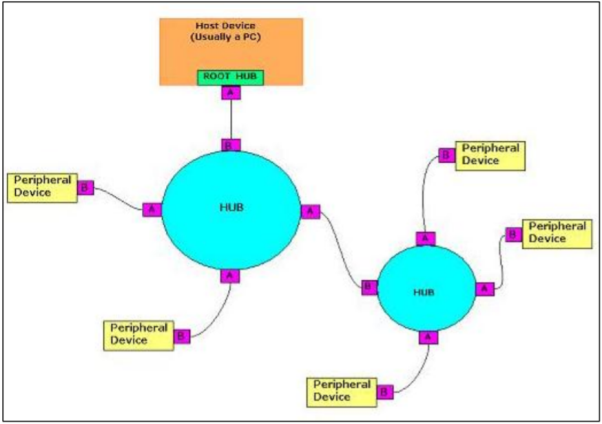
USB connectors: connecting a USB device to a computer is very simple. You find the USB connector on the back of your machine and plug to USB connector into it. If it is a new device, the operating system auto detect set and asks for the driver desk. If the device has already been installed, the computer activates it and starts talking to it. The USB standard specifies two kinds of cables and connectors, as shown below. The USB standard uses A and B connectors mainly to avoid confusion: A connectors head upstream towards the computer, B connectors, head down streams and connect to individual devices. By using different connectors on the upstream and downstream end, it is impossible to install a cable incorrectly, because the two types are physically different.

USB can support for data transfer types or transfer mobiles. Control isochronous bulk interrupt. Next paragraph. Control transfers, exchange configuration setup, and command information between the device and host. The host can also send commands or query parameters, with control packets. Isochronous transfer is used. My time Critical commerce streaming device. Such a speakers, video cameras. It s time sensitive information. So, within limitations, it has guaranteed access to the USB. Bulk transfer is used by devices like printers and scanners, which receives data in one big packet. Interrupt transfer, is used by peripherals exchanging small amount of data that need immediate attention. All USB data send serial. USB data transfer is essential in the form of packets of data commerce send back and forth between the host and peripheral devices. Initially, all packets are sent from the host, via the root hub and possibly more hubs, to devices. Each USB data transfer consists of
1 Token packet
2 Optional Data Packet
3 Statis Packet
Water Level Controller using 8051 Microcontroller project will help in automatically controlling the water motor by sensing the water level in a tank. This article explains you how to detect and control the water level in an overhead tank or any other container. This system monitors the water level of the tank and automatically switches ON the motor whenever tank is empty.
The motor is switched OFF when the overhead tank or container is FULL. Here, the water level of the tank is indicated on LCD (Liquid crystal Display). Using this system, we can avoid the overflow of the water.
We have already seen How water level indicator circuit works using AVR Microcontroller in the earlier post. But, here we are designing the circuit which is used to detect and control the water level automatically in overhead tank using 8051 microcontroller.
In this system, water sensing can be done by using a set of 4 wires, which are placed at different levels in tank. DC supply probe is placed at the base of the tank.
Circuit Principle
This system mainly works on a principle that “water conducts electricity”. The four wires which are dipped into the tank will indicate the different water levels. Based on the outputs of these wires, microcontroller displays water level on LCD as well as controls the motor.
Initially when the tank is empty, LCD will display the message LOW and motor runs automatically. When water level reaches to half level, now LCD displays HALF and still motor runs.
When the tank is full, LCD displays FULL and motor automatically stops. Again, the motor runs when water level in the tank becomes LOW.
Components Required for Water Level Controller using 8051 Microcontroller
- AT89C51 Microcontroller (or any 8051 based Microcontroller)
- 8051 Programmer (Programming Board)
- 11.0592 MHz Quartz Crystal
- 2 x 33pF Capacitor
- 2 x 10KΩ Resistor (1/4 Watt)
- 10µF Capacitor
- Push Button
- 1KΩ x 8 Resistor Pack (for Pull – up)
- 16 x 2 LCD Display
- 5V Relay
- 4 x 2N2222 (NPN) Transistors
- DC Motor (for demonstration)
- 10KΩ Potentiometer
- 1N4007 PN Junction Diode
- Programming cable
- Connecting wires
- Power Supply
- Keil µVision IDE
- Willar Software (for burning code)
- Proteus (for circuit diagram)
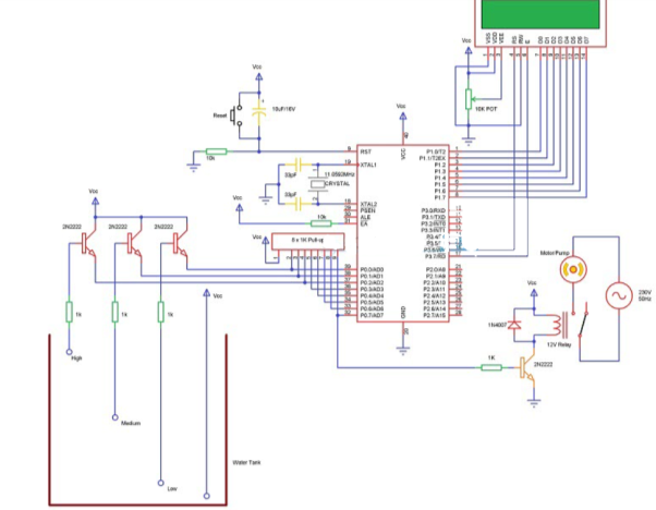
The heart of the Water Level Controller using 8051 Microcontroller project is the AT89C51 Microcontroller. The water level probes are connected to the P0.0, P0.1 and P0.2 through the transistors (they are connected to the base of the transistors through corresponding current limiting resistors). P0.0 for LOW level, P0.1 for HALF Level and P0.2 for HIGH Level.
The Collector terminals of the Transistors are connected to VCC and the Emitter terminals are connected to PORT0 terminals (P0.0, P0.1 and P0.2).
PORT1 of the microcontroller is connected to the data pins of LCD and the control pins RS, RW and EN of the LCD Display are connected to the P3.6, GND and P3.7 respectively.
For demonstration purpose, we have used a simple DC Motor Pump. It is connected to the Relay and the input to the relay is fed from P0.7 through a transistor.
Algorithm for Water Level Controller Circuit
- First configure the controller pins P0.0, P0.1 and P0.2 as inputs and P0.7 as output.
- Now, initialize the LCD.
- Continuously check the water level input pins P0.0, P0.1 and P0.2.
- If all the pins are low, then display tank as “EMPTY” on the LCD and make P0.7 pin HIGH to run the motor automatically.
- If the level is low i.e. if P0.0 is HIGH, display the water level as “LOW” and continue to run the motor.
- A HIGH pulse on the pin P0.1 indicates that water has reached half level. So, display the same thing on LCD and run the motor normally.
- If P0.2 is HIGH, then the water level in the tank is FULL.
- Now, make the P0.7 pin as LOW to turn off the motor automatically.
References:
1. The 8051 Microcontroller: A System Approach by Muhammad Mazidi, 1st Ed., PHI, 2012
2. D. M Calcutt, Fredrick J. Cowan " 8051 microcontroller: an application based introduction".
3. Subrata Ghoshal "8051 microcontroller" Pearson Education