Unit - 3
Integrated Development Environment (IDE) for Microcontrollers
Editors or text editors are software programs that enable the user to create and edit text files. In the field of programming, the term editor usually refers to source code editors that include many special features for writing and editing code. Notepad, Wordpad are some of the common editors used on Windows OS and vi, emacs, Jed, pico are the editors on UNIX OS. Features normally associated with text editors are — moving the cursor, deleting, replacing, pasting, finding, finding and replacing, saving etc.
Types of Editors
There are generally five types of editors as described below:
1. Line editor: In this, you can only edit one line at a time or an integral number of lines. You cannot have a free-flowing sequence of characters. It will take care of only one line.
Ex: Teleprinter, edlin, teco
2. Stream editors: In this type of editors, the file is treated as continuous flow or sequence of characters instead of line numbers, which means here you can type paragraphs.
Ex: Sed editor in UNIX
3. Screen editors: In this type of editors, the user is able to see the cursor on the screen and can make a copy, cut, paste operation easily. It is very easy to use mouse pointer.
Ex: vi, emacs, Notepad
4. Word Processor: Overcoming the limitations of screen editors, it allows one to use some format to insert images, files, videos, use font, size, style features. It majorly focuses on Natural language.
5. Structure Editor: Structure editor focuses on programming languages. It provides features to write and edit source code.
Ex: Netbeans IDE, gEdit.
What influence relocation requirement of a program?
Ans: Addressing Structure of Computer System.
How to reduce relocation requirement of a program?
Ans: By using that of the segmented addressing of the structure.
JUMP avoids use of that of the absolute address; hence instruction is no more that of the address sensitive.
Thus, no relocation is needed.
Effective Operand Address would be calculated considering starting address as 2000 would be <CS> + 0196 = 2196 (which is corrected address)
Let’s take example to understand it more clearly.
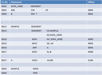
Example:
- Code written in assembly language for Intel 8088.
- ASSUME statements declare segment register CS and DS for memory addressing.
- So, all memory addressing is performed using suitable displacement of their contents.
- Translation time address of A is 0196.
- In statement 16, reference of A due to JMP statement makes displacement of 196 from the content of CS register.
- Hence avoids usage of that of the absolute addressing. Thus, instruction is not address sensitive. Displacement->avoids usage of absolute address->not address sensitive instruction.
- As DS is loaded with that of the execution time address of DATA_HERE, reference to B would be automatically relocated to correct address.
- Thus, Use of segment register reduces relocation requirement but doesn’t eliminate it.
- Inter Segment Calls & Jumps are handled in similar way.
- Relocation is more involved in case of intra segment jumps assembled in FAR format.
- Linker computes both: Segment Base Address–Offset of External Symbol
- Thus, no reduction in linking requirements.
Loader is special program that takes input of object code from linker, loads it to main memory, and prepares this code for execution by computer. Loader allocates memory space to program. Even it settles down symbolic reference between objects. It in charge of loading programs and libraries in operating system. The embedded computer systems don’t have loaders. In them, code is executed through ROM. Generally, loader has three types of approach:
1. Absolute loading
2. Relocatable loading
3. Dynamic run-time loading
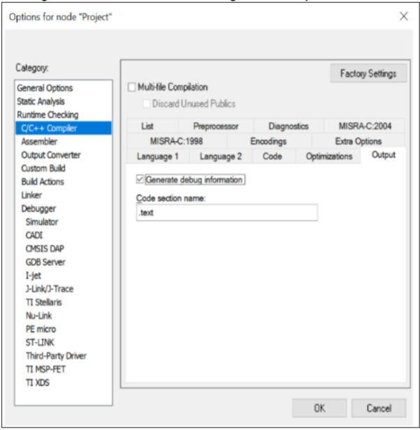
Debugging information is generated by the compiler together with the machine code. It is a representation of the relationship between the executable program and the original source code. This information is encoded into a pre-defined format and stored alongside the machine code. Debugging information is mandatory to set breakpoint or get the content of a variable. This chapter presents the location of the Debugging Information related option in IAR Systems®, Keil®, and STM32CubeIDE.
IAR™ EWARM “Generate debug information” option tick box is accessible in
Project -> Options -> C/C++ Compiler -> Output Pane
It is set by default.
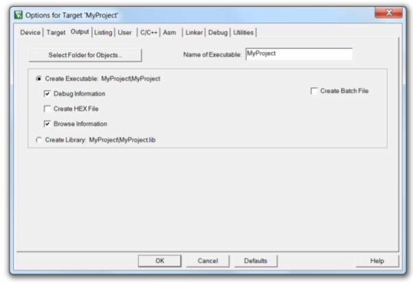
Keil®-MDK-Arm µVision Debug Information Tick box is accessible in
Project -> Options -> Output Pane.
It is set by default.
STM32CubeIDE Option to manage Debugging Information are in
Properties -> C/C++ Build -> Settings -> Tool Settings -> Debugging
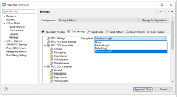
Debug Level can be set among four levels:
- None: Level 0 produces no debug information at all;
- Minimal (-g1): Level 1 produces minimal information, enough for making backtraces in parts of the program for which no debug is planned. This includes descriptions of functions and external variables, and line number tables, but no information about local variables.
- Default (-g): Produce debugging information in the operating system's native format (stabs, COFF, XCOFF, or DWARF). GDB can work with this debugging information.
- Maximal (-g3): Level 3 includes extra information, such as all the macro definitions present in the program. Some debuggers support macro expansion when -g3 is used
A circuit for emulating target system remains independent of a particular targeted system and processor. Emulator or ICE provides great flexibility and ease for developing various applications on a single system in place of testing that multiple targeted systems.
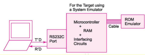
- Emulates MCU inputs from sensors
- Emulates controlled outputs for the peripheral interfaces/systems
- Emulates target MCU IOs and socket to connect externally MCU
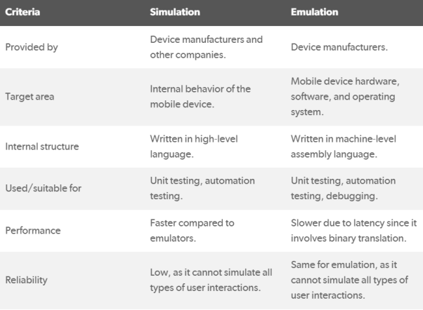
A simulator creates an environment that mimics the behavior and configurations of a real device. On the other hand, an emulator duplicates all the hardware and software features of a real device.
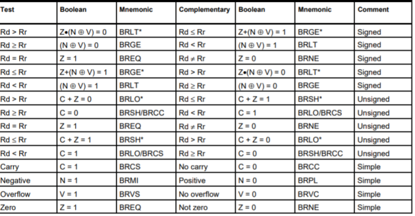
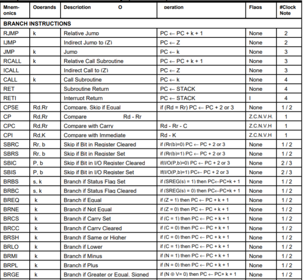
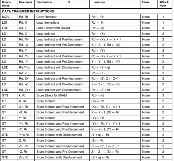
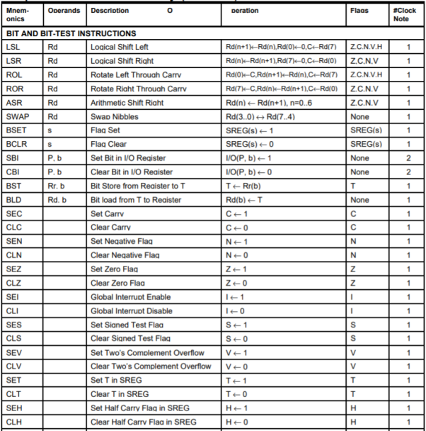
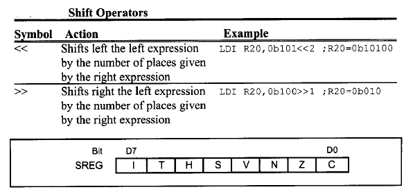
Status Register (SREG):
SREG: Status register
C: Carry flag in status register
Z: Zero flag in status register
N: Negative flag in status register
V: Twos complement overflow indicator
S: N ⊕ V, For signed tests
H: Half Carry flag in the status register
T: Transfer bit used by BLD and BST instructions
I: Global interrupt enable/disable flag Registers and operands:
Rd: Destination (and source) register in the register file
Rr: Source register in the register file
R: Result after instruction is executed
K: Constant literal or byte data (8 bit)
k: Constant address data for program counter
b: Bit in the register file or I/O register (3 bit)
s: Bit in the status register (3 bit)
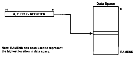
X,Y,Z: Indirect address register (X=R27:R26,
Y=R29:R28 and Z=R31:R30)
P: I/O port address
q: Displacement for direct addressing (6 bit)
I/O Registers RAMPX, RAMPY, RAMPZ: Registers concatenated with the X, Y and Z registers enabling indirect addressing of the whole SRAM area on MCUs with more than 64K bytes SRAM.
Stack:
STACK: Stack for return address and pushed registers
SP: Stack Pointer to STACK Opcode:
X: Don’t care
Flags: ⇔: Flag affected by instruction
0: Flag cleared by instruction
1: Flag set by instruction
-: Flag not affected by instruction
While instructions tell the CPU what to do, directives give directions to the assembler. The directives help us to develop our program easier and make our program legible.
.EQU (equate)
This is used to define a constant value or a fixed address. The. EQU directive does not set aside storage for a data item, but associates a constant number with a data or an address label. So that when the label appears in the program it’s constant will be substituted for the label the following uses .EQ you for the counter constant and constant is used to load the R21 register.
.EQU COUNT
………
LDI R21, COUNT
.SET
This directive is used to define a constant value or are fixed address in this regard the .SET and .EQU directives are identical the only difference is that the value assigned by the .SET directive may be reassigned later.
.ORG (origin)
The.org directive is used to indicate the beginning of the address it can be used for both code and data.
.INCLUDE directive
The .INCLUDE directive tells the AVR assembler to add the contents of a file to our program.
For example in the following program R24 is loaded with 29 which is the result of the arithmetic expression.
.EQU C1=0X50
.EQU C2=0X10
.EQU C3= 0X04
For example, suppose we want to set the zed and see bids of the SREG register and clear the others we load zero be 00000011 to SREG the task will be done
LDI R20, 0b00000011; Z=1, C=1
OUT SREG, R20
Macro definition
.Macro directive indicates the beginning of the macro definition and .END Macros directive signals the end. Everywhere Micro definition list have three parts as follows
.MACRO name
.END MACRO
There are applications in assembly language programming in which group of instructions perform a task that is used repeatedly. For example, moving data into a RAM location is done repeatedly in the same program. It doesn’t make sense to rewrite this code every time it is needed. Therefore, to reduce the time. That it takes to write code and reduce the possibility of error. The concept of macros was born. Macros allow the programmer to write that task once only and to invoke it whenever it is needed.
A macro can take up to ten parameters. The parameters can be referred to as at the rate 02 at the rate 9:00 in the body of the macro. After the macro has been written, it can be invoked by its name and appropriate values are substituted for parameters. For example, moving immediate data into I/O register data are am is a widely used service, but there is no instruction for that. We can use a macro to do the job. As shown in the following code.
.MACRO LOADIO
LDI R20, @1
OUT @0, R20
.ENDMACRO
.LISTMAC DIRECTIVE
When viewing the dot lst file with macros, the details of the macros are not displayed. This means that the bodies of the macros are not displayed when they are invoked during the code. But when we are debugging the code, we might need. To see exactly what instructions our executive using the .LISTMAC Directive weekend, turn on the display of the bodies of macros in the list file. For example.
.INCLUDE “M32DEF.INC”
.MACRO LOADIO
LDI R20,@1
OUT @0,R20
.ENDMACRO
LOADIO PORTA, 0X20
LOADIO DDRA, 0X53
HERE: JMP: HERE
If we add .LISTMAC directive to above code we have
.MACRO LOADIO
LDI R20, @1
OUT @0, R20
.ENDMACRO
.LISTMAC
LOADIO PORTA, 0X20
LOADIO DORA, 0X53
HERE: JMP: HERE
Macros v/s subroutines
Macros and subroutines are useful in writing assembly programs, but each has limitations. Macros increase court size every time they are involved. For example, if you call 10 instruction macro 10 times, the court size is increased by 100. Instructions, whereas if you call the same subroutine ten times, the court size is only that of the subroutine instructions. On the other hand, a function called takes 3 or four clocks. And the RET instruction takes for clocks to get executive. So, using functions adds around eight clock cycles. The subroutine you stack space as well when called. While the macros do not.
Example
Write quotes to set PB2 and PB4 of PORTB to 1 and clear the other pins i) without the directive and b) using the directive
a) Without directives
LDI R20, 0X14
OUT PORTB, R20
LDI R20,0b00010100
OUT PORTB, R20
b) With directives
LDI R20, (1<<4) | (1<<2); R20 = (0b10000| 0b00100) =0b10100
OUT PORTB, R20; PORTB= R20
As we already know the names of the register beds are defined in the header files of each AVR microcontroller PB2 and PB4 are defined equal to 2 and 4 as well therefore we can write the code as shown below
LDI R20, (1<< PB4) | (1<< PB2); set the PB4 and PB2 bits
OUT PORTB, R20; PORTB = R20
Q2) What does the abr assembler do while assembling the following program .EQU C1 =2
.EQU C2 = 3
LDI R20, C1 | (1<<C2); R20 = 2| (1<<3) = 0b00000010 | 0b00001000 = 0b00001010
A2) .EQU is an assembler directive when assembling .EQU C1 =2 assembler assigns value to 2 to C1. Similarly while assembling the .EQU C2=3 instruction it assigns the value 3 to C2
When the assembler converts instruction LDI R20, C1 | (1<<C2) to machine language it knows the value of C1 and C2. Thus, it calculates the value of C1| (1<<C2) and then replaces the expression with its value. Therefore, LDI R20, C1 | (1<<C2) will be converted to LDI R20, 0b00001010. Then the assembler converts the instructions to machine language.
The CPO can access data in various ways that the data could be in a register or in a memory are provided as an immediate value these various ways of accessing data are called addressing modes the various addressing modes of a microprocessor are determined when it is designed and therefore cannot be changed by the programmer the avr provide a total of 13 distinct addressing modes which can be categorized into following groups
1) single register or immediate
2) register
3) direct
4) Register indirect
5) Flash direct
6) Flash indirect
Single register or immediate addressing mode
In this addressing mode the operand is registered see example below change paragraph
NEG R18; negate the content of R18
COM R19; complement the contents of R19
INC R20: increment R20
DEC R21; decrement R21
ROR R22; rotate right R22
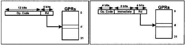
The constant value is sometimes referred to as immediate address since the operand comes immediately after the opcode when instruction is assembled and the addressing mode is referred to as immediate addressing mode in some microcontrollers but the AVR data sheet refers to this mode as a subject of the single register addressing mode. This addressing mode can be used to load data into any of the R16 - R31 general purpose register the immediate addressing mode is also used for arithmetic and logical instructions note that the letter capital I in instructions such as LDI, ANDI, and SUBI means immediate.
Two register addressing mode
This mode involves the use of two registers to hold the data to be manipulated.

ADD R20, R23; add R23 to R20
SUB R29, R20; subtract R20 from R29
AND R16, R17; AND R16 with 0 x 40
MOV R23, R19; copy contents of R19 to R23
Direct addressing mode
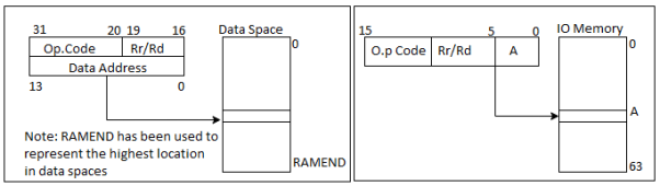
The entire data memory can be accessed using either direct or register indirect addressing modes. The direct addressing mode the operand data is in a RAM memory location whose address is known and this address is given as a part of the instruction contrast with the immediate addressing mode in which the operand data itself provides with the instruction as shown in figure the address field is a 16 bit address and can value from $0000 $ FFFF. Of course it is much easier to use names instead of addresses in the program and we have seen many examples of them in the last few chapters it must be noted that data memory does not support immediate addressing mode in order to move the data into internal RAM or to I/O register we must first move it to a GPR R16-R31 and then move it from the GPR to the data memory space using the STS instruction for example if we want to store 0X 95 in memory location 0x 520 we should write the following program
LDI R19, 0X95; load 0x95 into R19
STS 0X520, R19; store R19 into data location 0x520
I/O direct addressing mode
To access the I /O register there is a special mode called I /O direct addressing mode the I /O direct addressing mode can address only the standard I /O registers. The IN and OUT instructions use this addressing mode as shown in the figure the address field is a 6-bit address and can take the value from $002 $3 F which is from 00 to 63 in decimal so it can address the entire standardised slash register memory space AVR register from Ports A B and so on are part of the group registers commonly referred to as I/O registers there are many I/O register and they can be widely used. The I/O register can be accessed by their names or by their address.
OUT 0X15, R19; is the same as the next instruction
OUT PORTC, R19; which means copy R19 into PORT C
IN R26, 0X16; is the same as the next instruction
IN R26, PINB; which means copy PINB into R26
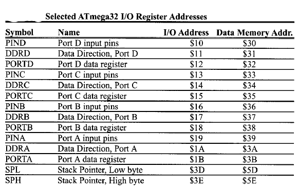
The address between $0 and $5 F of the data space has been assigned to standard I/O register. In all of the AVR these I/O register have to address as I/O address and data memory address. The I/O address is used when we use the io direct addressing mode while the data memory address is used when we use the direct addressing mode in other words the standard I/O register can be accessed using both the direct addressing and bio addressing mod. Some AVR have less than 64 I origins cats show some locations of the standard io memory are not used by the I/ O register the unused location are reserved and must not be used by the AVR programmer. Some AVR have more than 64 I/O Register.
The extra I/O registers are located above the data memory address $5 off the data memory allocated to the extra I/O registers is called extended I/O memory to access the extended I/O register. We can use the direct addressing mode for example in ATmega128 PORT F has the memory address of 0x 62. The I/O register can have different addresses in different AVR microcontroller for example the I/O address $2 is assigned to TWAR in the ATmega32 while the same address is assigned to de are in ATmega128 this means that in Atmega32 the instruction OUT 0X 2, R20 copies the content of R20 to TWAR while the same instruction in ATmega128 copy the content of R20 to DDRE.
Example
Write code to send $55 to PORTB. Include (a) the register name (b) the I/O address and (c) the data memory address?
a) LDI R20, 0XFF; R20 = 0XFF
OUT DDRB, R20; DDRB= R20 (Port B output)
LDI R20, 0X55; R20= $55
OUT PORTB, R20; Port B =0X55
b) LDI R20, 0XFF; R20 = 0XFF
OUT 0X17, R20; DDRB= R20 (Port B output)
LDI R20, 0X55; R20= $55
OUT 0X18, R20; Port B =0X55
c) LDI R20, 0XFF; R20 = 0XFF
STS 0X37, R20; DDRB= R20 (Port B output)
LDI R20, 0X55; R20= $55
OUT 0X38, R20; Port B =0X55
Register Indirect Addressing Mode
We can use direct or register indirect addressing mode to access data stored in the data memory the register indirect addressing mode is a very important addressing mode in the AVR. In register indirect addressing mode register is used as a pointer to the data memory location in the AVR three registers are used for this purpose X, Y and Z. These are 16-bit registers allowing access to the entire 65536 bytes of data memory space. In the AVR each of the registers is made by combining 2 specific GPRs for example combining R26 and R27 makes the X register. In this case R26 is the lower bite of X and R27 is the higher byte. The Y and Z registers are made by combining R29: R28 and R31:R30 respectively. The 16-bit registers X, Y and Z are widely used as pointer we can use them with the LD instruction to read the value of the location pointer to buy these registers. For example, the following instruction reads the value of the location pointer to buy the X pointer.
LD R24, X; load into R24 from location pointed to by X
Example
Write a program to copy the value $55 into memory locations $140 through $144 using (i) direct addressing mode (ii) register indirect addressing mode without loop and (iii) a loop
a) LDI R17,0X55; load R17 with value 0x55
STS 0X140, R17; copy R17 to memory location 0x140
STS 0X141, R17; copy R17 to memory location 0x141
STS 0X142, R17; copy R17 to memory location 0x142
STS 0X143, R17; copy R17 to memory location 0x143
STS 0X143, R17; copy R17 to memory location 0x144
b) LDI R16, 0X55; load R16 with value 0x55
LDI YL, 0X40; load R28 with value 0x40
LDI YH, 0X1; load R29 with value 0x1
ST Y, R16; copy R16 to memory location 0x140
INC YL; increment lower byte of Y
ST Y, R16; copy R16 to memory location 0x141
INC YL; increment the pointer
ST Y, R16; copy R16 to memory location 0x142
INC YL; increment the pointer
ST Y, R16; copy R16 to memory location 0x143
INC YL; increment the pointer
ST Y, R16; copy R16 to memory location 0x144
c) LDI R16, 0X5; R16=5
LDI R20, 0X55; load R20 with 0x55
LDI YL, 0X40; load YL with 0x 40
LDI YH,0X1; load YH with 0x1
L1:ST Y, R20; copy R20 to memory pointed to by Y
INC YL; increment the pointer
DEC R16; decrement the counter
BRNE L1; loop while counter is not 0
Assume that RAM locations $90-$94 have a string of ASCII data as shown below
$90 =(‘H’), $91 =(‘E’), $92 =(‘L’), $94 =(‘O’),
WAP to get each character and send it to port B one byte at a time. Show that the program using (a) Direct addressing mode (b) Register indirect addressing mode.
a) Using direct addressing mode
LDI R20, 0XFF;
OUT DDRB, R20; make Port B an output
LDS R20, 0X90; R20=content of location 0x90
OUT PORTB, R20; PORTB =R20
LDS R20, 0X91; R20=content of location 0x91
OUT PORTB, R20; PORTB =R20
LDS R20, 0X92; R20=content of location 0x92
OUT PORTB, R20; PORTB =R20
LDS R20, 0X93; R20=content of location 0x93
OUT PORTB, R20; PORTB =R20
LDS R20, 0X94; R20=content of location 0x94
OUT PORTB, R20; PORTB =R20
b) Using register indirect addressing mode
LDI R16, 0X5; R10= 0X5
LDI R20, 0XFF
OUT DDRB, R20; make port B an output
LDI ZL, 0X90; the lower byte of address (ZL=0x90)
LDI ZH, 0X0; the higher byte of address (ZL=0x0)
L1: LD R20, Z; read from location pointed to by Z
INC ZL; increment pointer
OUT PORTB, R20; send to Port B the contents of R20
DEC R16; decrement counter
BRNE L1; if R16 is not zero go to L1
WAP to clear 16 memory locations starting at data memory address $60. Use the following (a) INC Rn (b) Auto-increment.
a) LDI R16, 16; R16= 16 (counter value)
LDI XL, 0X60; XL = the low byte of address
LDI XH, 0X00; XH = the high byte of address
LDI R20, 0X0; R20=0
L1:ST X, R20; clear location X points to
INC XL; increment pointer
DEC R16; decrement counter
BRNE L1; loop until counter = 0
b) LDI R16, 16; R16= 16 (counter value)
LDI XL, 0X60; XL = the low byte of address
LDI XH, 0X00; XH = the high byte of address
LDI R20, 0X0; R20=0
L1:ST X+, R20; clear location X points to
DEC R16; decrement counter
BRNE L1; loop until counter = 0
Assume that data memory locations $240-$243 have following hex data. WAP to add them together and place the result in locations $220 and $221
$240 =(‘$7D’), $241 =(‘$EB’), $242 =(‘$C5’), $243=(‘$5B’)
.INCLUDE “M32DEF.INC”
.EQU L_BYTE = 0X220; RAM loc for L_Byte
.EQU H_ BYTE= 0X221; RAM loc for H_Byte
LDI R16,4
LDI R20,0
LDI R21,0
LDI XL,0X40; the low byte of x= 0x40
LDI XH, 0X20; the high byte of x= 02
L1: LD R22, X+; read content of location where X points to
ADD R20, R22
BRCC L2; branch if C=0
INC R21; increment R21
L2: DEC R16; decrement counter
BRNE L1; loop until counter is 0
ST L_BYTE, R20; store the low byte of the result in $220
ST H_BYTE, R21; store the high byte of the result in $221
WAP to copy a block of 5 bytes of data from data memory locations starting at $130 to RAM locations starting at $60.
LDI R16, 16; R16= 16 (counter value)
LDI XL, 0X30; the low byte of address
LDI XH, 0X01; the high byte of address
LDI YL, 0X60; the low byte of address
LDI YH, 0X00; the high byte of address
L1: LD R20, X+; read where X point to
ST Y+, R20; store R20 where Y points to
DEC R16; decrement counter
BRNE L1; loop until counter = zero
WAP to copy a block of 5bytes of data from data memory locations using ar $130 to RAM locations starting at $60.
LDI R16, 16; R16=16
LDI XL, 0X30; the low byte of address
LDI XH, 0X01; the high byte of address
LDI YL, 0X60; the low byte of address
LDI YH, 0X00; the high byte of address
L1: LD R20, X+; read where X points to
ST Y+, R20; store R20 where Y points to
DEC R16; decrement counter
BRNE L1; loop until counter =0
Two multibyte numbers are stored in locations $130-$133 and $150-$153. WAP to add thee multibyte numbers and save the result in address $160-$163.
$C7659812
+ $2978742A
.INCLUDE “M32DEF.INC”
LDI R16, 4; R16=4 counter value
LDI XL, 0X30
LDI XH, 0X1; load pointer Z= $130
LDI YL, 0X50
LDI YH, 0X1; load pointer Z= $150
LDI ZL, 0X60
LDI ZH, 0X1; load pointer Z= $160
CLC; clear carry
L1: LD R18, X+; copy memory to R18 and INC X
LD R19, Y+; copy memory to R19 and INC Y
ADC, R18, R19; R18= R18+R19+carry
ST Z+, R18; store R18 in memory and INC Z
DEC R16; decrement counter
BRNE L1; loop until counter =0
Write a function that adds the contents of three continuous locations of data space and stores the result in the first location. The Z register should point to the first location before the function is called?
.INCLUDE”M32DEF.INC”
LDI R16, HIGH
OUT SPH,R16
LDI R16, LOW
OUT SPL, R16
LDI ZL, 0X00
LDI ZH, 2
CALL ADD3LOC
HERE: JMP HERE
ADD3LOC:
LDI R21, 0
LD R20, Z
LDD R16, Z+!
ADD R20, R16
BRCC L1
INC R21
L1: LDD R16, Z+2
ADD R20, R16
BRCC L2
INC R21
L2: ST Z, R20
STD Z+1, R21
RET
Write a program to subtract 18H from 29 H and store the result in R21. Without using the SBI instruction and using the SUBI instruction.
a) Without SUBI instruction
LDI R21, 0X29
LDI R22, 0X18
SUB R21, R22
b) LDI R21, 0X29
SUBI R21, 0X18
Write a program to subtract two 16-bit numbers. 2762 H -1296 H assume R26 = 62 and R27 = 27. Place the difference in R26 and R 27 are 26. Should have the lower byte.
; R26=62
; R27= 27
LDI R28, 0X96
LDI R29, 0X12
SUB R26, R28
SBC R27, R29
Assume that the data memory location 0x315 has well do FD H. Write a program to convert it to decimal. Save the digits in location 0X322, 0X 323, zero X3 to 4 and where the least significant digit is in location 0X322
.EQU HEX_NUM = 0X315
.EQU RMND_L= 0X322
.EQU RMND_M= 0X323
.EQU RMND_H= 0X324
.DEF NUM= R20
.DEF DENOMINATOR = R21
.DEF QUOTIENT = R22
LDI R16, 0XFD
STS HEX_NUM, R16
LDS NUM, HEX_NUM
LDI DENOMINATOR, 10
L1: INC QUOTIENT
SUB NUM, DENOMINATOR
BRCC L1
DEC QUOTIENT
ADD NUM, DENOMINATOR
STS RMND_L, NUM
MOV NUM, QUOTIENT
LDI QUOTIENT, 0
L2: INC QUOTIENT
SUB NUM, DENOMINATOR
BRCC L2
DEC QUOTIENT
ADD NUM, DENOMINATOR
STS RMND_M, NUM
STS RMND_H, QUOTIENT
HERE: JMP: HERE
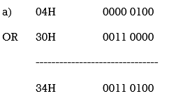
a) Show the results of the following
LDI R20, 0X04
ORI R20, 0X30
b) Assume that PB2 is used to control an outdoor light, and PB5 to control a light inside a building. Show how to turn “on” the outdoor light and turn “off” the inside one.
b) SBI DDRB,2; bit 2 of Port B is output
SBI DDRB, 5; bit 5 of Port B is output
IN R20, PORTB
ORI R20, 0b00000100
ANDI R20, 0b11011111
OUT PORTB, R20
HERE: JMP: HERE
Read and test port be to see whether it has the value 45H. If it does send 99 H to PORTC. Otherwise, it is clear.
LDI R20, 0XFF; R20 = 0xFF
OUT DDRC, R20; Port C is output
LDI R20, 0X00; R20= 0
OUT DDRB, R20; Port B is input
OUT PORTC, R20; PORTC =00
LDI R21, 0X45; R21= 45
HERE:
IN R20, PINB; get a byte
EOR R20, R21; Ex-or with 0x45
BRNE HERE
LDI R20, 0X99; R20 =0x99
OUT PORTC, R20; POTRC =99H
EXIT: JMP: EXIT; stop here
Write a program to monitor port. Be continuously for the value 63H. It should stop monitoring only if PORT B equals 63H
LDI R20, 0X00
OUT DDRB, R20
LDI R21, 0X63
AGAIN:
IN R20, PINB
CP R20, R21
BRNE AGAIN
Assume that won’t be is an input port connected to a temperature sensor. Write a program to read the temperature and test it for the value 75. According to the test results, place the temperature value into the registers indicated by the following.
If T=75 then R16=T ; R17=0; R18 =0
If T>75 then R16=0 ; R17=T; R18 =0
If T<75 then R16=0 ; R17=0; R18 =T
LDI R20, 0X00
OUT DDRB, R20
CLR R16
CLR R17
CLR R18
IN R20, PINB
CPI R20, 75
BRSH SAME_HI
MOV R18, R20
RJMP CNTNU
SAME_HI
BRNE HI
MOV R16, R20
RJMP CNTNU
HI:
MOV R17, R20
CNTNU: ………...
Write a program to add 2 signed numbers. The numbers are in R21 and R 22. The program should store the result in R 21. If the result is not correct, the program should put 0XAA on port. A and clear R21.
LDI R21, 0XFA
LDI R22, 0X05
LDI R23, 0XFF
OUT DDRA, R23
ADD R21, R22
BRVC NEXT
LDI R23, 0XAA
OUT PORTA, R23
LDI R21, 0X00
NEXT: ……...
Write a program to transfer the value 41 H serially. WAP in PB 1 put one high at the start and end of the data. Send the LSB first.
.INCLUDE”M32DEF.INC”
SBI DDRB, 1
LDI R20, 0X41
CLC
LDI R16, 8
SBI PORTB, 1
AGAIN:
ROR R20
BRCS ONE
CBI PORTB, 1
JMP NEXT
ONE: SBI PORTB, 1
NEXT:
DEC R16
BRNE AGAIN
SBI PORTB, 1
HERE: JMP HERE
WAP that find the number of 1s in a given byte
.INCLUDE “M32DEF.INC”
LDI R20, 0X97
LDI R30, 0
LDI R16, 8
AGAIN:
ROR R20
BRCC NEXT
INC R30
NEXT:
DEC R16
BRNE AGAIN
ROR R20
HERE: JMP HERE
WAP to bring in a byte of data serially via pin RC7 and save it in R20 register. The byte comes in with the LSB first.
.INCLUDE ”M32DEF.INC”
CBI DDRC, 7
LDI R16, 8
LDI R20, 0
AGAIN:
SBIC PINC, 7
SEC
SBIS PINC, 7
CLC
ROR R20
DEC R16
BRNE AGAIN
HERE: JMP HERE
When we talk about ‘embedded systems’, what do we mean? Opinions vary. Throughout this book, we will use the following loose definition: 1 chapter1 Programming embedded systems in C An embedded system is an application that contains at least one programmable computer (typically in the form of a microcontroller, a microprocessor or digital signal processor chip) and which is used by individuals who are, in the main, unaware that the system is computer-based.
Typical examples of embedded applications that are constructed using the techniques discussed here
- Mobile phone systems (including both customer handsets and base stations).
- Automotive applications (including braking systems, traction control, airbag release systems, engine-management units, steer-by-wire systems and cruise control applications).
- Domestic appliances (including dishwashers, televisions, washing machines, microwave ovens, video recorders, security systems, garage door controllers).
- Aerospace applications (including flight control systems, engine controllers, autopilots and passenger in-flight entertainment systems).
- Medical equipment (including anaesthesia monitoring systems, ECG monitors, drug delivery systems and MRI scanners).
- Defence systems (including radar systems, fighter aircraft flight control systems, radio systems and missile guidance systems).
When desktop developers first think about working with embedded systems, there is a natural inclination to stick with what they know and look for a book which uses Pentium processors or other devices from this family (such as the 80486, or the Intel 188). However, if you open up the engine management unit or the airbag release system in your car, or take the back off your dishwasher, you will not find any of these processors sitting inside, nor will there be anywhere to plug in a keyboard, graphics display or mouse. Typical desktop processors cost more than US $100.00 a piece (often much more). This cost puts them out of reach of all but the most expensive embedded application. (Who would pay more than US $100 for a TV remote-control unit?) In addition, a desktop processor requires numerous external support chips in order to function: this further increases the cost. The additional components also increase the physical size of the system, and the power consumption: both of these factors are major problems for battery-powered embedded devices. (Who would buy a portable music player that requires ten large batteries to run, and needs a trolley to transport it?)
Overall, the state-of-the art technology used in desktop processors matches the needs of the PC user very well: however, their key features – an ability to execute industry-standard code at a rate of more than 1000 million instructions per second – come with a heavy price tag and are simply not required in most embedded systems. The 8051 device is very different. It is a well-tested design, introduced in its original form by Intel in 1980. The development costs of this device have now been fully recovered, and prices of modern 8051 devices now start at less than US $1.00. At this price, you get a performance of around 1 million instructions per second, and 256 bytes (not megabytes!) of on-chip RAM. You also get 32 port pins and a serial interface. The 8051’s profile (price, performance, available memory, serial interface) match the needs of many embedded systems very well. As a result, it is now produced in more than 400 different forms by a diverse range of companies including Philips, Infineon, Atmel and Dallas. Sales of this vast family are estimated to have the largest share (around 60%) of the microcontroller market as a whole, and to make up more than 50% of the 8-bit microcontroller market. Versions of the 8051 are currently used in a long list of embedded products, from children’s toys to automotive systems.
Building a desktop PC from an 8051 would not be a practical proposition, but it is an excellent device for building many embedded systems. One important factor is that the 8051 requires a minimum number of external components in order to operate
The different nature of the embedded and desktop markets is emphasized by the fact that some of the more recent 8051 devices – far from being more powerful and having more features than the 1980 original – actually have fewer feature. By contrast, the more recent ‘Small 8051’ devices typically have only some 15 I/O pins, and do not support external memory. These devices are finding their way into applications that would have involved a small number of discrete components (transistors, diodes, resistors, capacitors) a few years ago, but which may now be implemented more cheaply using microcontrollers
Both the Standard and Small 8051s are aimed, largely, at low-performance application areas, where limited memory is required, and one of the most important considerations is product cost. This forms a large segment of the embedded market but – of course – not all projects take this form. To develop applications requiring additional hardware or larger amounts of memory, we can opt to switch to a 16-bit (or 32-bit) microcontroller environment – or even consider using a desktop microprocessor. However, such a move can require a major investment in staff, training and development tools. An alternative is to use one of the Extended 8051 devices introduced in recent years by a range of manufacturers.
One important application area for Extended 8051s has been the automotive sector. Recent economic, legislative and technological developments in this sector mean that an increasing number of road vehicles contain embedded systems. Linking these systems together in many recent vehicles is a low-cost, two-wire Controller Area Network (CAN) computer bus. The CAN bus eliminates the expensive (and heavy) multi-wire looms, shaving around US $600 or more from production costs: a significant saving.
In order to connect to the CAN bus, the various devices – from door mirrors to braking systems – each require an embedded processor. As a consequence, a modern passenger car may typically have 50 processors on board. To use 50 desktop chips in these circumstances, we would need to spend around US $5000. This cost greatly outweighs any saving achieved through the use of the CAN bus in the first place: in addition, the desktop processor would not have on-chip support for CAN, so additional hardware would be needed in order to provide this, further increasing our costs and design complexity. As an alternative, various Extended 8051s have on-chip hardware support for CAN.
The final thing to note about the 8051 architecture is that, if none of the 400 or so existing chips matches the needs of your application, you can now build your own device. For example, the Triscend3 E5 series of devices have 8051 cores, plus an additional area of field-programmable gate arrays (FPGAs) with which you can create your own ‘on chip’ hardware. Alternatively, for even greater flexibility, Xilinx Foundation4 provides a comprehensive set of tools for the programming of ‘blank’ FPGAs or Application-Specific ICs (ASICs). Compatible with these tools are a small range of 8051 ‘cores’ which can be purchased – for example – from Dolphin Integration.5 The use of such techniques allows you to create your own completely customized 8051 microcontroller, in order to match precisely your particular requirements.
Overall, the low cost, huge range, easy availability and widespread use of the 8051 architecture makes it an excellent platform for developing embedded systems: these same factors also make it an ideal platform for learning about embedded systems. Whether you will subsequently use 8-, 16- or 32-bit embedded processors, learning to work within the performance and memory limits of devices such as the 8051 is a crucial requirement in the cost-conscious embedded market. You simply cannot acquire these skills by developing code for a Pentium (or similar desktop) processor
● Computers (such as microcontroller, microprocessor or DSP chips) only accept instructions in ‘machine code’ (‘object code’). Machine code is, by definition, in the language of the computer, rather than that of the programmer. Interpretation of the code by the programmer is difficult and error prone.
● All software, whether in assembly, C, C++, Java or Ada must ultimately be translated into machine code in order to be executed by the computer.
There is no point in creating ‘perfect’ source code, if we then make use of a poor translator program (such as an assembler or compiler) and thereby generate executable code that does not operate as we intended.
● Embedded processors – like the 8051 – have limited processor power and very limited memory available: the language used must be efficient.
● To program embedded systems, we need low-level access to the hardware: this means, at least, being able to read from and write to particular memory locations (using ‘pointers’ or an equivalent mechanism).
● No software company remains in business for very long if it generates new code, from scratch, for every project. The language used must support the creation of flexible libraries, making it easy to re-use (well-tested) code components in a range of projects. It must also be possible to adapt complete code systems to work with a new or updated processor with minimal difficulty.
● Staff members change and existing personnel have limited memory spans. At the same time, systems evolve and processors are updated. As concern over the ‘Year 2000’ problem in recent years has illustrated, many embedded systems have a long lifespan. During this time, their code will often have to be maintained. Good code must therefore be easy to understand now, and in five years’ time (and not just by those who first wrote it).
● The language chosen should be in common use. This will ensure that you can continue to recruit experienced developers who have knowledge of the language. It will also mean that your existing developers will have access to sources of information (such as books, training courses, WWW sites) which give examples of good design and programming practice
● It is ‘mid-level’, with ‘high-level’ features (such as support for functions and modules), and ‘low-level’ features (such as good access to hardware via pointers).
● It is very efficient.
● It is popular and well understood.
● Even desktop developers who have used only Java or C++ can soon understand C syntax.
● Good, well-proven compilers are available for every embedded processor (8-bit to 32-bit or more).
● Experienced staff are available.
● Books, training courses, code samples and WWW sites discussing the use of the language are all widely available. Overall, C’s strengths for embedded system development greatly outweigh its weaknesses. It may not be an ideal language for developing embedded systems, but it is unlikely that a ‘perfect’ language will ever be created.
An Integrated Development Environment (IDE) is a software application that provides a programming environment to streamline developing and debugging software. Rather than performing all the steps required to make an executable program as unrelated individual tasks, it brings all the tools needed into one application and workspace. Each of the tools has an awareness of the environment, and they work together to present a seamless development set for the developer.
Even a simple search for IDEs will turn up quite a few choices. IDEs are available from Open Source communities, vendors, and software companies. They range from free to pricing dependent upon the number of licenses required. There isn't a standard for IDEs and each has its own capabilities, along with strengths and weaknesses. Generally, an IDE provides an easy-to-use interface, automates development steps, and allows developers to run and debug programs all from one screen. It can also provide the link from a development operating system to an application target platform, like a desktop environment, smartphone or microprocessor.
Software Development Steps
In any environment, to develop executable software you need to create source file(s), compile the source files to produce machine code (object files), and link the object files with each other and any libraries or other resources required to produce an executable file.
Source files contain the code statements to do the tasks your program is being created for. They contain program statements specific to the language you are using. If programming in c, the source files contain c code statements; java source files contain java statements. Usually, source files names have extensions indicating the code they contain. A c source file may be named "myfile.c". Compilers translate the source files to appropriate machine level code for the target environment. Linkers take all the object files required for a program and link them together, assigning memory and registers to variables, setting up data. They also link in library files to support operating system tasks and any other files the program needs. Linkers output executable files.
Compiler is a software tool that converts a source code written in a high level language on top of a particular operating system running on a specific target processor architecture (e.g. Intel x86/Pentium). Here the operating system, the compiler program and the application making use of the source code run on the same target processor. The source code is converted to the target processor specific machine instructions. The development is platform specific (OS as well as target processor on which the OS is running). Compilers are generally termed as 'Native Compilers'. A native compiler generates machine code for the same machine (processor) on which it is running. Cross-compilers are the software tools used in cross-platform development applications. In cross-platform development, the compiler running on a particular target processor/OS converts the source code to machine code for a target.
Embedded system development is a typical example for cross-platform development where embedded firmware is developed on a machine with Intel/AMD or any other target processors and the same is converted into machine code for any other target processor architecture (e.g. 8051, PIC, ARM, etc). Keil C51 is an example for cross-compiler. The term 'Compiler' is used interchangeably with 'Cross-compiler' in embedded firmware applications. Whenever you see the term 'Compiler' related to any embedded firmware application, please understand that it is referring to the cross-compiler.
Compiler | Cross Compiler |
A software that re translates the computer code writing in written in high level programming language to machine language. | A software that can create executable code for platforms other than the one on which the compiler is running. |
Helps to convert the high level source code into machine understandable machine code. | A type of compiler that can create executable code for different machines other than the machine it runs on. |
An internet service provider (ISP) is a corporation that provides both personal and business customers with internet access. For a charge, ISPs allow their customers to browse the web, shop online, conduct business, and communicate with family and friends.
Other services that ISPs can offer include email, domain registration, web hosting, and browser packages. Based on the services it provides, an ISP can also be referred to as an information service provider, a storage service provider, an internet service provider (INSP), or any combination of these terms.
During the mid-1990s, the number of ISPs grew to several thousand, and the bubble was in full swing. The internet economy arose as access opportunities expanded and speeds shifted away from slower dial-up connections. Customers can now get high-speed access via broadband technology via cable and digital subscriber line (DSL) modems, thanks to advances in provider technology.
ISPs typically give their customers the ability to communicate with one another through Internet email accounts, which are usually set up with several email addresses at the customer's discretion.
Other services can be offered, such as telephone and television services, as well as personal websites or home pages. Each ISP's services and service combinations can be special.
Internet service providers mainly provide their customers with internet access—basic access providers that only manage traffic between the user and the entire internet. However, depending on the customer's position and availability, additional resources could be included.
Among the programs available are:
● Email services
● Web hosting services
● Domain registration
● Browser and software packages
Key takeaway:
- An internet service provider (ISP) is a corporation that provides both companies and customers with access to the internet.
- Other services that ISPs can offer include email, domain registration, web hosting, and browser services.
- An internet service provider (ISP) may be classified as an information service provider, a storage service provider, an internet network service provider (INSP), or a combination of the three.
WAP to (a) clear R20 then (b) add 3 to R20 ten times and (c) send the sum to PORTB. Use the zero flag and BRNE
.INCLUDE”M32DEF.INC”
LDI R16, 10
LDI R20, 0
LDI R21, 3
AGAIN: ADD R20, R21
DEC R16
BRNE AGAIN
OUT PORTB, R20
WAP to (a) load the PORTB register with the value 0x55 and (b) complement Port B 700 times
.INCLUDE”M32DEF.INC”
.ORG 0
LDI R16, 0X55
OUT PORTB, R16
LDI R20, 10
LOP_1: LDI R21, 70
LOP_2: COM R16
OUT PORTB, R16
DEC R21
BRNE LOP_2
DEC R20
BRNE LOP_1
Find the sum of the values 0x79, 0xF5 and 0XE2. Put the sum into R20 and R21.
.INCLUDE “M32DEF.INC”
.ORG 0
LDI R21, 0
LDI R20, 0
LDI R16, 0X79
ADD R20, R16
BRSH N_1
INC R21
N_1: LDI R16, 0XF5
ADD R20, R16
BRSH N_2
INC R21
N_2: LDI R16, 0XE2
ADD R20, R16
BRSH OVER
INC R21
OVER:
Toggle all the bits of Port B by sending to it the values $55 and $AA continuously. Put a time delay between each issuing of data to Port B.
.INCLUDE ”M32DEF.INC”
.ORG 0
LDI R16, HIGH
OUT SPH, R16
LDI R16, LOW
OUT SPL, R16
BACK:
LDI R16, 0X55
OUT PORTB, R16
CALL DELAY
LDI R16, 0XAA
OUT PORTB, R16
CALL DELAY
RJMP BACK
Delay subroutine
.ORG 0X300
DELAY LDI R20, 0XFF
AGAIN:
NOP
NOP
DEC R20
BRNE AGAIN
RET
Find the size of the delay of the code snippet below if the crystal frequency is 10MHz.
DELAY: LDI COUNT, 0XFF
AGAIN: NOP
NOP
DEC COUNT
BRNE AGAIN
RET
Therefore, we have a time delay of [1+((1+1+1+2) x 255) + 4] x 0.1  s = 128.0
  s
s
WAP to toggle all the bits of I/O register PORTB every 1s. Assume that the crystal frequency id 8MHz and the system is using an ATmega32.
.INCLUDE “M32DEF.INC”
.ORG 0
LDI R16, HIGH
OUT SPH, R16
LDI R16, LOW
OUT SPL, R16
LDI R16, 0X55
BACK:
COM R16
OUT PORTB, R16
CALL DELAY_1S
RJMP BACK
DELAY_1S
LDI R20, 32
L1: LDI R21, 200
L2: LDI R22, 250
L3:
NOP
NOP
DEC R22
BRNE L3
DEC R21
BRNE L2
DEC R20
BRNE L1
RET
Machine cycle= 1/8 MHz = 125ns
Delay = 32 x 200 x 250x 5x 125ns = 1000000000 ns = 1000000  s
s
In this calculation we have not included the overhead associated with the two outer loops.
References:
1. The AVR Microcontroller and Embedded Systems: A System Approach by Muhammad A. Mazidi, 1st Ed., PHI, 2013.
2. Kenneth J. Ayala, "The 8051 Microcontroller", Penram International Publishing, 1996.
3. Embedded C Programming and the ATMEL AVR by R H Barnett 2nd Ed., Cengage Learning Publication, 2006.


