Unit - 4
Introduction to other advanced microcontrollers
- An ARM processor is one of a family of CPUs based on the RISC (reduced instruction set computer) architecture developed by Advanced RISC Machines (ARM).
- ARM processors are extensively used in consumer electronic devices such as smart phones, tablets, multimedia players and other mobile devices, such as wearables.
Features
- This has high performance RISC CPU.
- 40-pin PDIP, high performance, enhanced Flash Microcontroller with CAN.
- The Operating speed ranges between 40 MHz up to 10 MIPS.
- The Operating voltage ranges 4.2 to 5.5 V
- ROM of size 2M bytes
- RAM between 256 bytes to 4096 bytes.
- On-chip program ROM in form of flash memory.
- Data EEPROM
- 8 x 8 Single cycle Hardware Multiplier
- 16-bit wide instructions, 8-bit wide data path.
- 75 instructions.
- ADC and USART PROTOCOL for PC communication.
- I/O port between 16 to 72 pins and I/O port register are bit and port accessible.
- SPI PROTOCOL and I2C PROTOCOL for memory communication.
- PIC 18F458 has two-stage pipeline.
- Interrupt capability with Priority levels.
- Linear program memory addressing upto 2 Mbytes
Selection:
- Speed
- Amount of RAM/ROM
- Numbers of I/O pins, Timers
- Power Consumption
- Tools of availability
- Added features like ADC/DAC/CCP, Bus support like CAN, SPI, I2C, USB.
- Watch Dog timer, Timer modes, Data EEPROM.
ARM Processors
ARM Processors can be divided into
- ARM Classic Processors: Arm classic processors include the Arm11, Arm9, and Arm7 processor families. These processors are still widely used around the globe, providing cost-effective solutions for many of today's applications.
- ARM Embedded Processors: Software development for embedded applications includes anything which uses a microcontroller or microprocessor to execute dedicated tasks on its own or within a larger system. Arm supports embedded software development at every stage of the project workflow.
- ARM Application Processors: Advanced RISC machine (ARM) is the first reduced instruction set computer RISC processor for commercial use, which is currently being developed by ARM holdings. ... ARM processor finds applications in digital TVs, set-top boxes, smart phones, mobile, laptops etc.
- ARM Classic processors include ARM7, ARM9 and ARM11 families and ARM7TMDI is still the highest shipping 32-bit processor. ARM7 based processors are still used in many small and simple 32-bit devices.
Version ARM 7:
- ARM7 is a group of older 32-bit RISC ARM processor cores licensed by ARM Holdings for microcontroller use.
- The ARM7 core family consists of ARM700, ARM710, ARM7DI, ARM710a, ARM720T, ARM740T, ARM710T, ARM7TDMI, ARM7TDMI-S, ARM7EJ-S. The ARM7TDMI and ARM7TDMI-S were the most popular cores of the family.
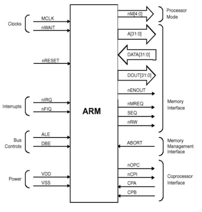
Fig. ARM7 FUNCTIONAL DIAGRAM
- The final thing that must be explained is how the ARM will be used and the way in which the chip appear.
- The various signals that interface with the processor are input, output or supervisory signals which will be used to control the ARM operation.
PIC
- This has high performance RISC CPU.
- 40-pin PDIP, high performance, enhanced Flash Microcontroller with CAN.
- The Operating speed ranges between 40 MHz up to 10 MIPS.
- The Operating voltage ranges 4.2 to 5.5 V
- ROM of size 2M bytes
- RAM between 256 bytes to 4096 bytes.
- On-chip program ROM in form of flash memory.
- Data EEPROM
- 8 x 8 Single cycle Hardware Multiplier
- 16-bit wide instructions, 8-bit wide data path.
- 75 instructions.
- ADC and USART PROTOCOL for PC communication.
- I/O port between 16 to 72 pins and I/O port register are bit and port accessible.
- SPI PROTOCOL and I2C PROTOCOL for memory communication.
- PIC 18F458 has two-stage pipeline.
- Interrupt capability with Priority levels.
- Linear program memory addressing upto 2 Mbytes
Characteristics 8-bit microcontroller with an integrated CAN module
1. A 32 k flash program memory,
2. A 1536-byte RAM data memory,
3. A 256-byte EEPROM memory,
4. Twenty two I/O ports,
5. Five-channel 10-bit A/D converters,
6. Three timers/counters,
7. Three external interrupt pins,
8. High current (25-mA) sink/source,
9. Capture/compare/Pulse Width Modulation (PWM) module,
10. SPI/I2C module,
11. CAN 2.0A/B module,
12. Power-on reset and power-on timer,
13. Watchdog timer,
14. Priority level interrupts,
15. DC to 40-MHz clock input,
16. An 8 × 8 hardware multiplier,
17. Wide operating voltage (2.0–5.5 V),
18. Power saving sleep mode.
Characteristics if 16 bit characteristics
CPU16
1. 16 Bit Architecture
2. Control-Oriented Digital Signal Processing Capability
3. 16 bit Multiply and Accumulate (digital signal processing)
4. 1 Megabyte of Program Memory Space and 1 Megabyte of Data Memory Space
5. High Level Language Support
6.Fast Interrupt Response Time
7. Hardware Breakpoint Signal
8. Background Debugging Mode (BDM)
9. Fully Static Operation
10. Watchdog Timer, Clock Monitor and Bus Monitor
11. Parallel Ports Option on Address and Data Bus in Single Chip Mode
12. Two 8 bit Dual Function Input/Output Ports
13. One 7 bit Dual Function Output Port
14. Phase-Locked Loop (PLL) Clock System
15. Multichannel Communication Interface (MCCI)
17. Two channels of enhanced Serial Communication Interface (SCI) (UART)
18. One channel of Serial Peripheral Interface (SPI)
19. Configurable Timer Module Version 7 (CTM7)
20. One 16 bit modulus counters (MCSM)
21. One 16 Bit Free-Running Counter (FCSM)
22. Six single-action submodules (SASM)
Key takeaways
- Twenty two I/O ports,
- High current (25-mA) sink/source
- DC to 40-MHz clock input
- Multichannel Communication Interface (MCCI)
- Two channels of enhanced Serial Communication Interface (SCI) (UART)
- Watchdog Timer, Clock Monitor and Bus Monitor
- Phase-Locked Loop (PLL) Clock System
- One 16 bit modulus counters (MCSM)
- This has high performance RISC CPU.
- 40-pin PDIP, high performance, enhanced Flash Microcontroller with CAN.
- The Operating speed ranges between 40 MHz up to 10 MIPS.
- The Operating voltage ranges 4.2 to 5.5 V
- ROM of size 2M bytes
- RAM between 256 bytes to 4096 bytes.
- On-chip program ROM in form of flash memory.
- Data EEPROM
- 8 x 8 Single cycle Hardware Multiplier
- 16-bit wide instructions, 8-bit wide data path.
- 75 instructions.
- ADC and USART PROTOCOL for PC communication.
- I/O port between 16 to 72 pins and I/O port register are bit and port accessible.
- SPI PROTOCOL and I2C PROTOCOL for memory communication.
- PIC 18F458 has two-stage pipeline.
- Interrupt capability with Priority levels.
- Linear program memory addressing upto 2 Mbytes
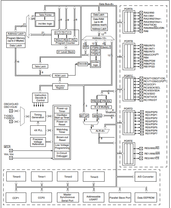
Figure. Architecture of PIC controller
The microcontroller architecture consists of CPU, I/O ports, memory organization, A/D converter, timers/counters, interrupts, serial communication, oscillator and CCP module
CPU (Central Processing Unit)
The PIC microcontroller CPU consists of the Arithmetic and Logic Unit, Memory Unit, Control Unit, accumulator and so on.
Arithmetic logic unit are mainly used for arithmetic operations and logical decisions. After processing, for storing the instructions memory is used. To control the internal and external peripherals, control unit is used to connect to CPU and accumulator is used for storing results.
Memory Organization
The memory module consists of RAM, ROM and STACK.
Random Access Memory (RAM)
RAM is an unstable memory used to store data temporarily in its registers. The registers of RAM are classified into Special Function Registers (SFR) and General-Purpose Registers (GPR).
- General Purpose Registers (GPR)
These registers are used for general purpose only.
- Special Function Registers
They are mainly used for special purposes only. These registers perform according to the functions assigned to them,
The STATUS register cannot be used for storing data, these registers are used for showing the operation or status of the program.
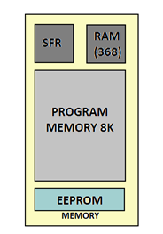
Figure. Memory Organization
Read Only Memory (ROM)
Read only memory is a stable memory used to store the data permanently. In PIC microcontroller ROM stores the instructions or programs. The microcontroller acts according to the program.
The ROM is also called as program memory, here the user writes the program and saves it permanently and executed by CPU. The microcontroller’s performance depends on the instruction executed by the CPU.
Electrically Erasable Programmable Read Only Memory (EEPROM)
Normally in ROM, we write the program only once and cannot use it multiple times. But, in EEPROM you can program the ROM multiple times.
Flash Memory
Flash memory also known as programmable read only memory (PROM) can read, write and erase the program thousands of times. PIC microcontroller uses this type of ROM.
Stack
When an interrupt occurs, first the PIC microcontroller must execute the interrupt and the existing process address that is being executed and store it in the stack. After completing the execution of the interrupt, the microcontroller calls the process with the help of address, which is stored in the stack and executes the process.
BUS
BUS is used for transfer and receive of data from one peripheral to another. It is classified into two types that is address and data bus.
Data Bus: It is used to transfer or receive the data.
Address Bus: Address bus transmits the memory address from peripherals to CPU. I/O pins are used to interface with external peripheral. UART and USART are serial communication protocols used for interfacing serial devices like GSM, GPS, Bluetooth, IR,and so on.

Figure. BUS
A/D converters
The analog to digital converter converts analog voltage values to digital voltage values. A/D module of PIC microcontroller consists of 5 inputs of 28 pin devices and 8 inputs of 40 pin devices.
The operation of the analog to digital converter is controlled by special registers ADCON0 and ADCON1. The upper bits of the converter are stored in ADRESH register and lower bits of the converter are stored in ADRESL register. It requires 5V of an analog reference voltage for operation.

Figure. A/D CONVERTER
Timers/ Counters
PIC microcontroller consists of four timer/counters wherein one is 8-bit timer and the remaining timers can be 8 or 16-bit mode. Timers are used for generating accuracy actions, for example, creating specific time delays between two operations.
Interrupts
PIC microcontroller consists of 20 internal interrupts and three external interrupt sources associated with different peripherals like ADC, USART, Timers, and so on.
Serial Communication
Serial communication is the method used for transferring data one bit at a time sequentially over communication channel.
- USART: (Universal synchronous and Asynchronous Receiver and Transmitter)
The two serial communication protocols used for transmitting and receiving data bit by bit over a single wire with respect to clock pulses. The PIC microcontroller has two pins TXD and RXD used for transmitting and receiving the data serially.
- SPI Protocol: (Serial Peripheral Interface)
This protocol is used for sending data between PIC microcontroller and other peripherals which include SD cards, sensors and shift registers.
PIC microcontroller supports three- wire SPI communications between two devices on a common clock source.
- I2C Protocol: (Inter Integrated circuit)
A serial protocol used to connect low speed devices such as EEPROMS, microcontrollers, A/D converters, and so on.
PIC microcontroller support two wire Interface or I2C communication between two devices which can work as Master and Slave device.
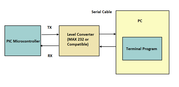
Figure. Serial Communication
CCP module
CCP module stands for capture/compare/PWM.
- Capture Mode: Capture mode captures the time of arrival of a signal, that is when the CCP pin goes high, it captures the value of Timer1.
- Compare Mode: Compare mode acts as analog comparator. When timer1 value reaches certain reference valueit generates output.
- PWM Mode: PWM mode provides pulse width modulated output with 10-bit resolution and programmable duty cycle.
Key takeaway
The microcontroller architecture consists of CPU, I/O ports, memory organization, A/D converter, timers/counters, interrupts, serial communication, oscillator and CCP module
The PIC microcontroller support only two addressing modes. They are
i) Direct addressing mode
Ii) Indirect addressing mode
Direct addressing mode
In this mode 7 bit of instruction identify the register file address and the 8th bit of register file address register bank select bit (RP0).
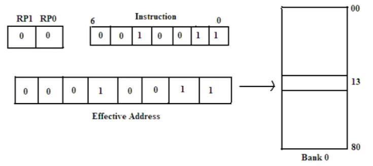
The above figure shows the method of accessing register file address 13H by direct addressing method.
Indirect addressing mode
Tn this addressing mode the 8-bit register file address is first written into a special function register (SFR) which acts as a pointer to any address location in the register file. A subsequent direct access of INDF will actually access the register file using the content of FSR pointer to the desired location of the operand.
Instruction set
i) Write the instructions mnemonics in lower case
Ii) Write special register names, RAM variable names and bit names in upper case
Iii) Write instruction and subroutine labels in mixed case.
The instruction set of PIC is divided into three basic categories
a) Byte oriented instruction
b) Bit oriented instruction
c) Literal and control instruction
Byte oriented Instructions
In this f represents the file register and d represents destination register. The destination specifies where the result of operation is to be placed. If D=0 the result is placed in W register and if d=1, the result is placed in the file register specified in the instruction.
ADDWF f, d
CLR f
MOVWF f, d
NOP
SUBWF f, b
Bit oriented Instruction
In this b represents a bit field designator which selects the number of the bit affected by the operation and f represents the number of the file in which the bit is located.
BCF f, b
BSF f, b
BTFSC f,b
Literal and Control Instruction
In literal and control instruction K represents an 8 or 11 bit constant or literal value.
ADDLW k
ANDLW k
CALL k
MOVLW k
SUBLW k
Clock System
Clock sources availability depends on the version of MSP430 microcontroller.
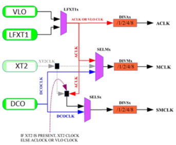
Figure. Clock System
VLOCCLK- This is a very low power/low frequency internal oscillator that can produce a frequency of 10KHz.
LFXT1CLK- (Low Frequency Crystal) – It is a crystal powered low/high frequency oscillator. It can work with either a 32Khz crystals that operate in the MHz range or external clock sources (400KHz to 16MHz range)
XT2CLK(High frequency crystal)- This is a high frequency oscillator that can be used with standard crystals resonator or external clock sources in the 400Khz to 16 MHz range.
DCOCLK- Integrated Digitally Controlled Oscillator do not use any external crystals. The DCO can generate a wide variety of frequencies ranging from few 100-kilo hertz to 10’s of MHz. It is default clock of the MSP430 after reset. The DCO clock frequency is temperature dependent.
MSP430 produces 3 different clock signals using a combination of the oscillator sources. These clock signals can be used to various peripherals like CPU, Timers, ADC etc depending upon the requirements.
MCLK- Known as main clock. It is fast high frequency clock usually used by CPU or other fast components like ADC10,ADC12, Watch Dog timer. MCLK can be sources either from LFT1CLK,DCO,VLO or XT2 oscillator. Clock signal can be divided by 1/2/4/8 using internal divider.
SMCLK- Known as Sub Main Clock. It can be sources either from LFT1CLK,DCO,VLO or XT2 oscillator. Clock signal can be divided by 1/2/4/8 using internal divider.
ACLK- known as Auxillary clock is slow, low frequency clock . It can only be sourced from LFT1CLK or VLO. Clock signal can be divided by 1/2/4/8 using internal divider. ALCK is active in all Low power modes except LPM4.
Low Power Modes
MSP430 works on two types of mode:
- Active Mode
- Low Power Modes(Standby mode)
MSP430 is designed for ultralow power applications. It offers the lowest power consumption and perfect mix of integrated peripherals for a variety of battery operated applications.
It has Low power modes LPM 0,1,2,3,4, and 3.5 and 4.5. AM is the normal running mode and all LPM for low power consideration modes. The low power operating modes consider the needs of ultralow-power consumption, speed, data throughput and minimization of individual peripheral current consumption.
LPM0- Both CPU and MCLK are disabled. SMCLK and ACLK remain active. Peripherals which use SMCLK and ACLK also remain active.
LPM1- Both CPU and MCLK are disabled. DCO is disabled. SMCLK is not available if it is sourced from DCO, ACLK remains active.
LPM2- CPU, MCLK, SMCLK and DCO are disabled, ACLK remain active.
LPM3 – CPU, MCLK, SMCLK, DCO are disabled, ACLK remain active.
LPM4- All the clocks including ACLK are disabled in this mode. The controller can only be wakened from this mode by an external interrupt. This mode consumes the least power compared to all other modes.
Clock Request Feature
The Launchpad typically uses a MSP430G2553 device that contains a Basic Clock Module+. XT1 supports both low frequency and high frequency crystals, and it integrates both DCOCLK and VLOCLK.
After power-up, MCLK and SMCLK are sourced from DCOCLK at about 1.1MHz. ACLK is sourced from LFXT1CLK in LF mode. The Launchpad comes with an option 32kHz crystal in the box that needs to be installed by the user.

Fig. Pin 18 and Pin 19 are XIN and XOUT and allow an external crystal to be connected, either 32kHz or a fast crystal.
The following code makes P2.6 and P2.7 set for accepting a crystal at the input:
MSP430 Using External 32kHz crystal
#include <msp430.h>
Void main()
{
WDTCTL = WDTPW + WDTHOLD; // Stop watchdog timer
P2SEL |= (BIT6 | BIT7); // Set P2.6 and P2.6 SEL for XIN, XOUT
P2SEL2 &= ~(BIT6|BIT7); // Set P2.6 and P2.7 SEL2 for XIN, XOUT
/* Select 32kHz Crystal for ACLK */
BCSCTL1 &= (~XTS); // ACLK = LFXT1CLK
BCSCTL3 &= ~(BIT4|BIT5); // 32768Hz crystal on LFXT1
/* Output buffered ACLK on P1.0 */
P1SEL |= BIT0;
P1SEL2 &= ~(BIT0);
P1DIR |= BIT0;
}
Low power programming and Interrupt
To enable low power the MSP430 supports several modes, each shutting off the MSP430 more and more:
- Active Mode (AM) – Not a low power mode but rather the mode in which everything is turned on, except perhaps for some peripherals
- LPM0 – CPU and MCLK are shutoff. SMCLK and ACLK remain active.
- LPM1 – CPU and MCLK are off, as in LPM1, but DCO and DC generator are disabled if the DCO is not used for SMCLK. ACLK is active.
- LPM2 – CPU, MCLK, SMCLK and DCO are disabled, while DC generator is still enabled. ACLK is active.
- LPM3 – CPU, MCLK, SMCLK, DCO and DC generator are disabled. ACLK is active.
- LPM4 – CPU and all clocks disabled
These LPM modes refer to the individual bits in the Status Register. By setting and clearing the bits in the SR, one can turn off CPU and clocks resulting in certain Low Power Modes.
To see the power consumption
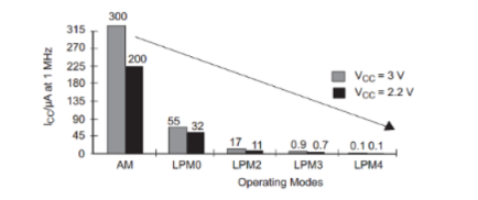
Figure. Power Consumption
At 1MHz, we go from 300uA down to less than 1uA by switching to LPM3. This is what makes the MSP430 such a good microcontroller for low power applications. It can survive for years on batteries.
Key Takeaway:
Low power operation is a key feature of the MSP430. Its design gives very low leakage, and it operates from a single supply rail.
References:
1. The 8051 Microcontroller: A System Approach by Muhammad Mazidi, 1st Ed., PHI, 2012
2. D. M Calcutt, Fredrick J. Cowan " 8051 microcontroller: an application based introduction".
3. Subrata Ghoshal "8051 microcontroller" Pearson Education