Unit - 3
Digital Modulation Techniques
(i) Generation
The QPSK Modulator uses a bit-splitter, two multipliers with local oscillator, a 2-bit serial to parallel converter, and a summer circuit.
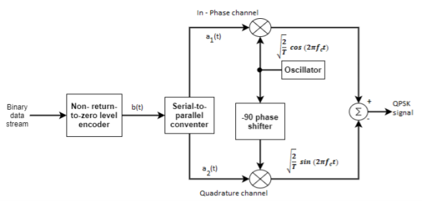
Fig 1: QPSK generation
At the modulator’s input, the message signal’s even bits (i.e., 2nd bit, 4th bit, 6th bit, etc.) and odd bits (i.e., 1st bit, 3rd bit, 5th bit, etc.) are separated by the bits splitter and are multiplied with the same carrier to generate odd BPSK (called as PSKI) and even BPSK (called as PSKQ). The PSKQ signal is anyhow phase shifted by 90° before being modulated.
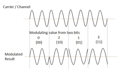
The QPSK waveform for two-bits input is as follows, which shows the modulated result for different instances of binary inputs.
(ii) Detection
The QPSK Demodulator uses two product demodulator circuits with local oscillator, two band pass filters, two integrator circuits, and a 2-bit parallel to serial converter.

Fig 2: QPSK detectors
The two product detectors at the input of demodulator simultaneously demodulate the two BPSK signals. The pair of bits are recovered here from the original data. These signals after processing are passed to the parallel to serial converter.

Fig 3: QPSK output
Error Calculation
In QPSK system the information carried by the transmitted signal is contained in the phase. The transmitted signals are given by


Where the carrier frequency fc=nc/7 for some fixed integer nc.
E = the transmitted signal energy per symbol.
T = Symbol duration.
The basic functions ɸ1(t) and ɸ2(t) are given by


There are four message points and the associated signal vectors are defined by

The table shows the elements of signal vectors, namely Si1 & Si2
Input dibit | Phase of QPSK signal (radians) | Coordinates of message points | Input dibit |
Si1 | Si2 | ||
10 | π/4 | +E/2 | -E/2 |
00 | 3π/2 | -E/2 | -E/2 |
01 | 5π/4 | +E/2 | +E/2 |
11 | 7π/4 | +E/2 | +E/2 |
Therefore, a QPSK signal is characterized by having a two-dimensional signal constellation (i.e., N=2) and four message points (i.e., M=4) as illustrated in figure.
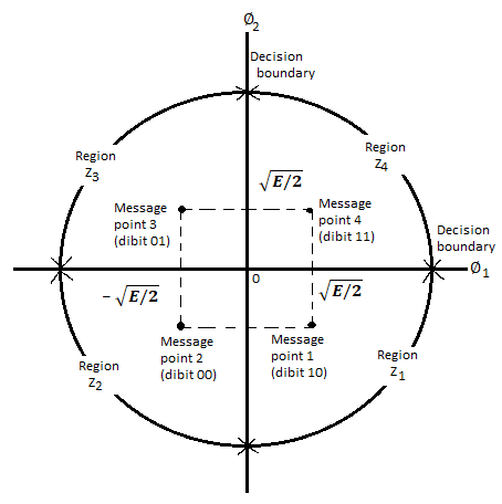
Fig 4. Signal-space diagram of coherent QPSK system
A QPSK system is in fact equivalent to two coherent binary PSK systems working in parallel and using carriers that are in-phase and quadrature. The in-phase channel output x1 and the Q-channel output x2 may be viewed as the individual outputs of the two coherent binary PSK systems. Thus, the two binary PSK systems may be characterized as follows
The signal energy per bit √E/2
The noise spectral density is No/2
The average probability of bit error in each channel of the coherent QPSK system is 

The bit errors in the I-channel and Q-channel of the QPSK system are statistically independent. The I-channel makes a decision on one of the two bits constituting a symbol (di bit) of the QPSK signal and the Q-channel takes care of the other bit. Therefore, the average probability of a direct decision resulting from the combined action of the two channels working together is pc= probability of correct reception p1= probability of error


The average probability of symbol error for coherent QPSK is given by
Pe = 1 – PC = 
In the region where E/2No We may ignore the second term and so the approximate formula for the average probability of symbol error for coherent QPSK system is

Key takeaway
QPSK Modulator uses a bit-splitter, two multipliers with local oscillator, a 2-bit serial to parallel converter, and a summer circuit.
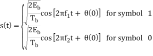
In the coherent detection of binary FSK signal, the phase information contained in the received signal is not fully exploited, other than to provide for synchronization of the receiver to the transmitter. We now show that by proper use of the continuous-phase property when performing detection, it is possible to improve the noise performance of the receiver significantly. Here again, this improvement is achieved at the expense of increased system complexity. Consider a continuous-phase frequency-shift keying (CPFSK) signal, which is defined for the signaling interval 0 t Tb as follows:

Where Eb is the transmitted signal energy per bit and Tb is the bit duration.
Another useful way of representing the CPFSK signal s(t) is to express it as a conventional angle-modulated signal:
s(t) =  cos [ 2πfct + θ(t)]
Where (t) is the phase of s(t) at time t. When the phase (t) is a continuous function of time, we find that the modulated signal s(t) is itself also continuous at all times, including the inter-bit switching times. The phase (t) of a CPFSK signal increases or decreases linearly with time during each bit duration of Tb seconds, as shown by
θ(t) = θ(0) ± (πh/Tb)t, 0 ≤ t ≤ Tb
Here the plus sign corresponds to sending symbol 1 and the minus sign corresponds to sending symbol 0; the dimensionless parameter h is to be defined. We deduce the following pair of relations:
fc + h/2TB = f1
fc – h/2TB = f2
Solving this pair of equations for fc and h, we get
fc = ½ (f1 + f2)
h – Tb (f1 – f2)
Signal-Space Diagram of MSK
Using a well-known trigonometric identity of conventional angle modulated signal, we may expand the CPFSK signal s(t) in terms of its in-phase and quadrature components as
s(t) =  cos θ (T) cos 2π fc t -
  sin θ (t) sin 2 π fct

Fig 5: Boldfaced path represents the sequence 1101000.
Consider, first, the in-phase component √2Eb/Tbcos(t)
θ(t) = θ(0) ± π/2Tb, 0 ≤ t ≤ Tb
Where the plus sign corresponds to symbol 1 and the minus sign corresponds to symbol 0. A similar result holds for (t) in the interval –Tb t 0, except that the algebraic sign is not necessarily the same in both intervals. Since the phase (0) is 0 or depending on the past history of the modulation process, we find that in the interval –Tb t Tb, the polarity of cos(t) depends only on (0), regardless of the sequence of 1s and 0s transmitted before or after t = 0. Thus, for this time interval, the in-phase component consists of the half-cycle cosine pulse:
s1(t) =  cos θ (t)
=  cos θ (0) cos (πt/2Tb)
= ±  cos (πt/2Tb ) - Tb ≤ t ≤ Tb
Where the plus sign corresponds to (0) = 0 and the minus sign corresponds to (0) = . In a similar way, we may show that, in the interval 0 t 2Tb, the quadrature component of s(t) consists of the half-cycle sine pulse:
sQ(t) =  sin θ (t)
=  sin θ (Tb) sin (πt/2Tb)
= ±  sin (πt/2Tb ) 0 ≤ t ≤ 2Tb
Where the plus sign corresponds to (Tb) = 2 and the minus sign corresponds to (Tb)=–2. From the discussion just presented, we see that the in-phase and quadrature components of the MSK signal differ from each other in two important respects:
- They are in phase quadrature with respect to each other and
- The polarity of the in-phase component sI(t) depends on (0), whereas the polarity of the quadrature component sQ(t) depends on (Tb).
Moreover, since the phase states (0) and (Tb) can each assume only one of two possible values, any one of the following four possibilities can arise:
1. (0) = 0 and (Tb) = /2, which occur when sending symbol 1.
2. (0) = and (Tb) = /2, which occur when sending symbol 0.
3. (0) = and (Tb) = –/2 (or, equivalently, 3/2 modulo 2), which occur when sending symbol 1.
4. (0) = 0 and (Tb) = –/2, which occur when sending symbol 0.
This fourfold scenario, in turn, means that the MSK signal itself can assume one of four possible forms, depending on the values of the phase-state pair: (0) and (Tb).
Signal-Space Diagram
We see that there are two orthonormal basis functions 1(t) and 2(t) characterizing the generation of MSK; they are defined by the following pair of sinusoidally modulated quadrature carriers:
1(t) = 2/Tb cos (πt/2Tb) cos (2πfct) 0≤ t ≤ Tb
2(t) = 2/Tb sin (πt/2Tb) sin (2πfct) 0≤ t ≤ Tb
s(t) = s11(t) + s11(t) 0≤ t ≤ Tb
Where the coefficients s1 and s2 are related to the phase states (0) and (Tb), respectively. To evaluate s1, we integrate the product s(t)1(t) with respect to time t between the limits –Tb and Tb, obtaining
s1 = 
= Eb cos [θ(0)] -Tb ≤ t ≤ Tb
Similarly, to evaluate s2 we integrate the product s(t)2(t) with respect to time t between the limits 0 and 2Tb, obtaining
s2 = 
From above two equations we conclude that
1. Both integrals are evaluated for a time interval equal to twice the bit duration.
2. The lower and upper limits of the integral used to evaluate s1 are shifted by the bit duration Tb with respect to those used to evaluate s2.
3. The time interval 0 t Tb, for which the phase states (0) and (Tb) are defined, is common to both integrals.
It follows, therefore, that the signal constellation for an MSK signal is two-dimensional (i.e., N = 2), with four possible message points (i.e., M = 4), as illustrated in the signal space diagram of Figure below.
( + Eb , + Eb), ( - Eb , + Eb), ( - Eb , - Eb) and ( + Eb , - Eb)
The possible values of (0) and (Tb), corresponding to these four message points, are also included in Figure below. The signal-space diagram of MSK is thus similar to that of QPSK in that both of them have four message points in a two-dimensional space. However, they differ in a subtle way that should be carefully noted:
- QPSK, moving from one message point to an adjacent one, is produced by sending a two-bit symbol (i.e., dibit).
- MSK, on the other hand, moving from one message point to an adjacent one, is produced by sending a binary symbol, 0 or 1. However, each symbol shows up in two opposite quadrants, depending on the value of the phase-pair: (0) and (Tb).

Fig 6: Signal-space diagram for MSK system
Generation and Coherent Detection of MSK Signals
With h = 1/2, we may use the block diagram of Figure(a) below to generate the MSK signal. The advantage of this method of generating MSK signals is that the signal coherence and deviation ratio are largely unaffected by variations in the input data rate. Two input sinusoidal waves, one of frequency fc = nc4Tb for some fixed integer nc and the other of frequency 14Tb, are first applied to a product modulator. This modulator produces two phase-coherent sinusoidal waves at frequencies f1 and f2, which are related to the carrier frequency fc and the bit rate 1/Tb in accordance with above equations for deviation ratio h = 12. These two sinusoidal waves are separated from each other by two narrowband filters, one centered at f1 and the other at f2. The resulting filter outputs are next linearly combined to produce the pair of quadrature carriers or orthonormal basis functions 1(t) and 2(t). Finally, 1(t) and 2(t) is multiplied with two binary waves a1(t) and a2(t), both of which have a bit rate equal to 1/(2Tb)
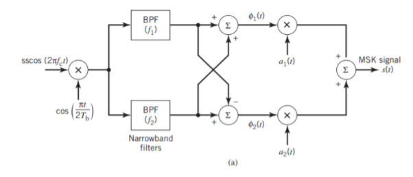

Fig 7: Block diagrams for (a) MSK transmitter and (b) coherent MSK receiver
Figure (b) above shows the block diagram of the coherent MSK receiver. The received signal x(t) is correlated with 1(t) and 2(t). In both cases, the integration interval is 2Tb seconds, and the integration in the quadrature channel is delayed by Tb seconds with respect to that in the in-phase channel. The resulting in-phase and quadrature channel correlator outputs, x1 and x2, are each compared with a threshold of zero
Error Probability of MSK
In the case of an AWGN channel, the received signal is given by
x(t) = s(t) + w(t)
Where s(t) is the transmitted MSK signal and w(t) is the sample function of a white Gaussian noise process of zero mean and power spectral density N0/2. To decide whether symbol 1 or symbol 0 was sent in the interval 0 t Tb, say, we have to establish a procedure for the use of x(t) to detect the phase states (0) and (Tb). For the optimum detection of (0), we project the received signal x(t) onto the reference signal over the interval –Tb t Tb, obtaining
x1 = 
w1 is the sample value of a Gaussian random variable of zero mean and variance N0/2. From the signal-space diagram, we see that if x1 > 0, the receiver chooses the estimate. On the other hand, if x1 0, it chooses the estimate. Similarly, for the optimum detection of (Tb), we project the received signal x(t) onto the second reference signal 2(t) over the interval 0 t 2Tb, obtaining
x2 =  0 ≤ t ≤ 2Tb
w2 is the sample value of another independent Gaussian random variable of zero mean and variance N02. Referring again to the signal space diagram, we see that if x2 0, the receiver chooses the estimate Tb= – 2. If, however, x2 0, the receiver chooses the estimate ˆ Tb = 2
It follows, therefore, that the BER for the coherent detection of MSK signals is given by
Pc = Q (2Eb/N0)
Key takeaway
- In M-ary PSK using coherent detection, increasing M improves the bandwidth efficiency, but the Eb/N0 required for the idealized condition of “error-free” transmission moves away from the Shannon limit as M is increased.
- In M-ary FSK, as the number of frequency-shift levels M is increased—which is equivalent to increased channel-bandwidth requirement—the operating point moves closer to the Shannon limit.
s(t) = A(t) cos(2πfct + θ(t) + θ)
A(t) = amplitude information
θ(t)= phase information
fc = the carrier frequency
θ = the phase shift introduced by the channel
- In coherent communications, θ is known to receivers
- In non-coherent communications, θ is unknown to receivers and assumed to be a random variable distributed uniformly over (-π, π)
- The phase shift is treated as a random variable distributed uniformly over (-π, π) and no phase estimation is provided at the receiver.
- We are now concerned with non-coherent communications
- The phase shift θ is the same during two consecutive signal transmission intervals
[(n-1)T, nT) and [nT, (n + 1)T).
- The information phase sequence {θn} is still differentially encoded as before.
- The transmitted signal s(t) in the interval [(n-1)T, (n +1)T] is

- θn = θn – θn-1 and θn-1 are independent. Both of them take values uniformly over
{0, 2π/M, . . ., 2π(M-1)/M}
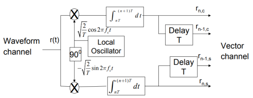
Fig 8: DPSK generation
rn,c = Es cos(θn + θ) + ηn,c , rn,s = Es sin(θn + θ) + ηn,s
ηn,c, ηn,s , ηn-1, c , ηn-1, s are i.i.d
Each of them ~ N(0, N0/2)
Key Takeaways:
Here, the phase of the modulated signal is shifted relative to the previous signal element. No reference signal is considered here. The signal phase follows the high or low state of the previous element. This DPSK technique doesn’t need a reference oscillator.
When the digital symbol modulates amplitude, phase or frequency of the carrier without any reference to previous symbol, it is called memory less modulations.
PAM
In PAM, amplitude of pulses is varied in accordance with instantaneous value of modulating signal.

Fig 9. PAM waveform
PAM Generation:
The carrier which is in the form of narrow pulses has frequency fc. The uniform sampling takes place in multiplier to generate PAM signal. Samples are placed Ts sec away from each other.

Fig 10. PAM Modulator
- The circuit is simple emitter follower.
- In the absence of the clock signal, the output follows input.
- The modulating signal is applied as the input signal.
- Another input to the base of the transistor is the clock signal.
- The frequency of the clock signal is made equal to the desired carrier pulse train frequency.
- The amplitude of the clock signal is chosen the high level is at ground level(0v)
- Low level at some negative voltage sufficient to bring the transistor in cutoff region.
- When clock is high, circuit operates as emitter follower and the output follows in the input modulating signal.
- When clock signal is low, transistor is cutoff and output is zero.
- Thus the output is the desired PAM signal.
PAM Demodulator:
The PAM demodulator circuit which is just an envelope detector followed by a second order op-amp low pass filter (to have good filtering characteristics) is as shown below

Fig 11. PAM Demodulator
Key takeaway
The carrier which is in the form of narrow pulses has frequency fc. The uniform sampling takes place in multiplier to generate PAM signal. Samples are placed Ts sec away from each other.
PWM and PPM
There are two types of PTM systems. They are Pulse width modulation (PWM) and Pulse Position Modulation (PPM).
Pulse Width Modulation
In this type of modulation, the amplitude is maintained constant but the width of each pulse is varied in accordance with instantaneous value of the analog signal. In PWM information is contained in width variation. This is similar to FM. In pulse width modulation (PWM), the width of each pulse is made directly proportional to the amplitude of the information signal.

Fig 12. PWM waveform
PPM
In this type of modulation, the sampled waveform has fixed amplitude and width whereas the position of each pulse is varied as per instantaneous value of the analog signal. PPM signal is further modification of a PWM signal.
PPM and PWM modulator
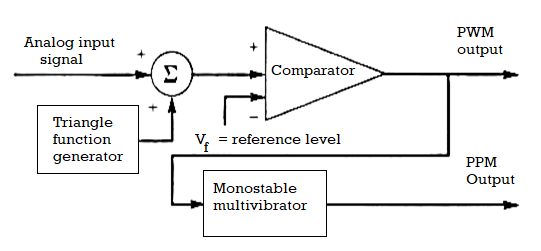
Fig 13. PTM Modulator
- The PPM signal can be generated from PWM signal.
- The PWM pulses obtained at the comparator output are applied to a mono stable multi vibrator which is negative edge triggered.
- Hence for each trailing edge of PWM signal, the monostable output goes high. It remains high for a fixed time decided by its RC components.
- Thus as the trailing edges of the PWM signal keeps shifting in proportion with the modulating signal, the PPM pulses also keep shifting.
- Therefore all the PPM pulses have the same amplitude and width. The information is conveyed via changing position of pulses.

Fig 14. PWM and PPM Modulation waveforms.
PWM Demodulator

Fig 15. PWM Demodulator
- Transistor T1 works as an inverter.
- During time interval A-B when the PWM signal is high the input to transistor T2 is low.
- Therefore, during this time interval T2 is cut-off and capacitor C is charged through an R-C combination.
- During time interval B-C when PWM signal is low, the input to transistor T2 is high, and it gets saturated.
- The capacitor C discharges rapidly through T2.
- The collector voltage of T2 during BC is low.
- Thus, the waveform at the collector of T2is similar to saw-tooth waveform whose envelope is the modulating signal.
- Passing it through 2nd order op-amp Low Pass Filter, gives demodulated signal.
PPM Demodulator
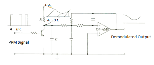
Fig 16. PPM Demodulator
- The gaps between the pulses of a PPM signal contain the information regarding the modulating signal.
- During gap A-B between the pulses the transistor is cut-off and the capacitor C gets charged through R-C combination.
- During the pulse duration B-C the capacitor discharges through transistor and the collector voltage becomes low.
- Thus, waveform across collector is saw-tooth waveform whose envelope is the modulating signal.
- Passing it through 2nd order op-amp Low Pass Filter, gives demodulated signal.
Key takeaway
In pulse time modulation system, we use the increased bandwidth consumed by pulses to obtain an improvement in noise performance by representing the sample values of the message signal by some property of pulse rather than amplitude.
Comparison between PAM, PPM and PWM
SR. NO. | PARAMETER | PAM | PWM | PPM |
1 | Type of Carrier | Train of Pulses | Train of Pulses | Train of Pulses |
2 | Variable Characteristic of the Pulsed Carrier | Amplitude | Width | Position |
3 | Bandwidth Requirement | Low | High | High |
4 | Noise Immunity | Low | High | High |
5 | Information Contained in | Amplitude Variations | Width Variations | Position Variations |
6 | Transmitted Power | Varies with amplitude of pulses | Varies with variation in width | Remains Constant |
7 | Need to transmit synchronizing pulses | Not needed | Not needed | Necessary |
8 | Complexity of generation and detection | Complex | Easy | Complex |
9 | Similarity with other Modulation Systems | Similar to AM | Similar to FM | Similar to PM |
10 | Output waveforms | Refer Figure down | Refer Figure down | Refer Figure down |
QAM
QAM (also known as QASK) is a combination of ASK and PSK. Here, both the amplitude and the phase are varied to transmit more bits per symbol.
The QAM modulator essentially follows the idea that can be seen from the basic QAM theory where there are two carrier signals with a phase shift of 90° between them. These are then amplitude modulated with the two data streams known as the I or In-phase and the Q or quadrature data streams. These are generated in the baseband processing area.
Basic QAM I-Q modulator circuit
The two resultant signals are summed and then processed as required in the RF signal chain, typically converting them in frequency to the required final frequency and amplifying them as required.

Fig.17: Basic QAM
It is worth noting that as the amplitude of the signal varies any RF amplifiers must be linear to preserve the integrity of the signal. Any non-linearities will alter the relative levels of the signals and alter the phase difference, thereby distorting he signal and introducing the possibility of data errors.
Basic QAM I-Q demodulator circuit
The basic modulator assumes that the two quadrature signals remain exactly in quadrature.
A further requirement is to derive a local oscillator signal for the demodulation that is exactly on the required frequency for the signal. Any frequency offset will be a change in the phase of the local oscillator signal with respect to the two double sideband suppressed carrier constituents of the overall signal.
Systems include circuitry for carrier recovery that often utilises a phase locked loop - some even have an inner and outer loop. Recovering the phase of the carrier is important otherwise the bit error rate for the data will be compromised.
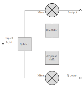
Fig 18: Basic QAM demodulator
The circuits shown above show the generic IQ QAM modulator and demodulator circuits that are used in a vast number of different areas. Not only are these circuits made from discrete components, but more commonly they are used within integrated circuits that are able to provide a large number of functions.
Error Probability
BER for QAM constellation
The SER for a rectangular M-QAM (16-QAM, 64-QAM, 256-QAM etc) with size L = M2 can be calculated by considering two M-PAM on in-phase and quadrature components. The error probability of QAM symbol is obtained by the error probability of each branch (M-PAM) and is given by

Signal Space Representation
For the case when M = 2k , k even, the resulting signal space diagram has a “square constellation.” In this case the QAM signal can be thought of as 2 PAM signals in quadrature. For M = 2k, k odd, the constellation takes on a “cross” form. For example, 16-QAM constellation is

Fig 19:16-QAM constellation
Key takeaway
QAM (also known as QASK) is a combination of ASK and PSK. Here, both the amplitude and the phase are varied to transmit more bits per symbol.
GENERATION AND COHERENT DETECTION OF BPSK SIGNALS
(i) Generation
To generate the BPSK signal, we build on the fact that the BPSK signal is a special case of DSB-SC modulation. Specifically, we use a product modulator consisting of two components.
(i) Non-return-to-zero level encoder, whereby the input binary data sequence is encoded inpolar form with symbols 1 and 0 represented by the constant-amplitude.
(ii) Product modulator, which multiplies the level encoded binary wave by the sinusoidal carrier of amplitude to produce the BPSK signal. The timing pulses used to generate the level encoded binary wave and the sinusoidal carrier wave are usually, but not necessarily, extracted from a common master clock.

(ii) Detection
To detect the original binary sequence of 1s and 0s, the BPSK signal at the channel output is applied to a receiver that consists of four sections
(a)Product modulator, which is also supplied with a locally generated reference signal thatis a replica of the carrier wave
(b)Low-pass filter, designed to remove the double-frequency components of the product modulator output (i.e., the components centered on) and pass the zero-frequency components.
(c)Sampler, which uniformly samples the output of the low-pass filter at where; the localclock governing the operation of the sampler issynchronized with the clock responsible for bit-timing in the transmitter.
(d)Decision-making device, which compares the sampled value of the low-pass filtersoutput to an externally supplied threshold, every seconds. If the threshold is exceeded, the device decides in favor of symbol 1; otherwise, it decides in favor of symbol 0. Levels.

The signal B is


QPSK
For Gray encoding,  can directly be computed.
Assume that  is transmitted which corresponds to
  Then the conditional bit error probability is given by


From the direct decision rule for data bits

 2=1⇔Y∈D2⋃D3
Thus,


By symmetry all conditional four bit errors probabilities are identical. Since two data bits are transmitted per modulation symbol (waveform) in QPSK, we have the relations  and .Therefore,


Offset Quadriphase-Shift Keying
QPSK : carrier phase may jump by ± 90° or ± 180° every 2 bit durations Problem : filtering action can cause the carrier amplitude to fluctuate → receiver produce additional symbol errors To reduce fluctuation → Offset Quadriphase-Shift Keying
Second substream m2 (t) is delayed (offset) by a bit duration T
Phase transitions are confined in 0°, ± 90°
π/4-Shifted Quadriphase-Shift Keying
Similar to Offset Quadriphase-Shift Keying (OQPSK) Carrier phase of QPSK can be (usually 1.):
1. 0, π/2, π or 3π/2
2. π/4, 3π/4, 5π/4 or 7π/4
The amplitude fluctuations during filtering are significantly reduced
• Reduced amplitude fluctuation becomes important when transmitter includes slightly nonlinear amplifier.
π/4-Shifted QPSK has been adopted in north American digital cellular time division multiple access (TDMA) standard IS-54 as well as the Japanese digital cellular standard.

CPFSK
In rectangular pulse shaping (Linear Pulse Shaping), phase changes linearly with the time, and the frequency is held constant throughout the data interval. In general, frequency pulse of length L is denoted by LREC. With L = 1, 1REC-CPM signal is called Continuous Phase Frequency Shift Keying (CPFSK). Note that although the rectangular pulse-shaping function is discontinuous, the phase response function is continuous. Frequency function f(t), of linear pulse shape with full response CPM (L = 1) signaling is given as:

And the corresponding phase function

So, for full response CPFSK,
(t, a)= aig(t – (i – 1)T) +θi, (i-1)T ≤ t ≤ iT,
θ(t, ai) = aig(t – (i – 1)T) = πhai(t – (i – 1)T)/T, (i – 1)T ≤ t ≤ iT
θi = πh  (i – 1)T ≤ t ≤ iT
In order to better understand CPFSK signals, we provide the following plots. Figure shows the phase state plot for 2-CPFSK with. It can be inferred from the Figure that the transmitted sequence is, based on the direction the signal moves in, or the slope of the signal within the bit interval. Figure shows the physical phase state, which is the observed phase. The jumps in the physical phase state are not discontinuities. They are the phase state but wrapped within the interval. Figures amplitudes are the normalized phase with respect to. No discontinuities are present due to the inherent memory characteristics of CPM signals. Figure shows the passband CPFSK signal. It can be noticed how frequency changes based on the data input, increasing with a +1 input and decreasing with -1 input. Moreover, the frequency change is noticed to be instantaneous at the beginning of each interval and holds its value for the rest of the bit interval
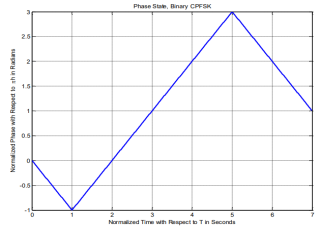
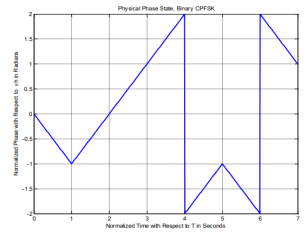
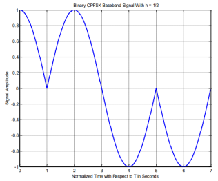
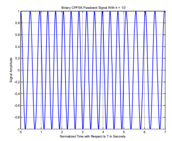
Figures above show the phase tree and phase trellis for 2-CPFSK and h= 1/2, respectively. We emphasize that the phase transitions in the state trellis diagram in Figure shows from one state to another are not true phase trajectories. They represent phase transitions for the terminal/observed states at the time instants t= (i-1)T, 1 i
i n.
n.
CPM
Continuous Phase Modulation (CPM) is a memory-type, constant-envelope, nonlinear modulation, which allows the use of power efficient low cost, nonlinear power amplifiers without introducing distortion. Digital transmission using constant-envelope CPM has become important because of its attractive properties. The constant-envelope designs are fairly immune to nonlinear channel effects. Although constructions of CPM are diverse in their properties and applications, they all rely upon the use of inherent memory introduced by the continuous phase. This constraint of continuous phase not only provides faster spectral roll-off, but also permits multiple symbol detection rather than the more conventional symbol-by-symbol detection. In this Chapter, two subclasses of CPM called Continuous Phase Frequency Shift Keying (CPFSK) and Continuous Phase Chirp Keying (CPCK) are described, although the treatment provided applies, in general, to any CPM. Concepts, mathematical descriptions and properties of CPM signals are presented with primary focus on CPFSK and CPCK signaling techniques.
The general form of a CPM signal is given by
s(t, a) = 2Eb/T cos(2πfct + (t, a) + 0), 0≤t≤nπ,
Where is the symbol energy, is the symbol duration, is the carrier frequency, is the initial phase offset which is assumed to be zero for coherent detection without any loss of generality. Is a sequence of independent and identically distributed M-ary information symbols each taking one of the  values with an equal probability of 1/M such that,
a = (a1, a2, . . . , an), ak ∈ { ±1, ±3, . . . , ±(M-1)}, 1≤k≤n,
Where and the phase function is defined as the integral of an instantaneous frequency pulse and is given by:
(t, a) =  (i – 1)T≤ t ≤iT,
g(t) = 2 π 
The derivative of g(t) is the frequency pulse shape f(t). That is

Where L is the frequency response pulse length. The frequency pulse length dictates the time interval over which a single input data symbol can affect the instantaneous frequency. Depending on the value of L, two different schemes of CPM can be defined. When L=1, the entire pulse extends over one full symbol interval. This type of CPM is known as full response CPM. When L>1, only a part of the pulse shape extends over a symbol and is known as partial response CPM signaling.
Generation of CPM

Data sequence passes through the pulse shaping filter and the multiplier to form frequency pulse sequence, which is then FM modulated to generate the CPM signal.
The phase of CPM can be represented by a tree structure. The tree structure is found by manipulating the information carrying phase. It can be viewed as the sum of two phase terms: instantaneous phase and accumulated phase. The phase of CPM signal during the ith symbol interval to give
(t, a) = 
= θ(t, ai) + θi (i – 1)T≤ t ≤iT,
θ(t, ai) = 
Which represents the changing part of the total phase during (i-1) T t
t iT and is determined by the current data symbols and previous L-1 symbols. The first term of Equation above, is dependent on the sequence of past input data symbols and the current data input (ai-L+1,….., ai-1) , and is called the correlative state. There are M L-1 possible correlative states. Since we are only interested in full response CPM , then
θ(t, ai) = aig(t – (i-1)T), (i – 1)T≤ t ≤iT
And is the accumulated phase, the phase state, which represents the constant part of the total phase in the same interval is
θi = g(t = T)  (i – 1)T≤ t ≤iT
The accumulated phase can be interpreted as the sum of the maximum phase changes contributed by each symbol, accumulated along the time axis up to the (i-1) symbol interval. It can be computed recursively as
θi+1 = θi + g(t = T)ai
The phase behavior of CPM signals can be best described by sketching the set of phase trajectories ɸ(t,a) generated by all possible values of the information sequence {ai} . These phase diagrams are called phase trees and they are specific to each CPM scheme, based on the different modulation parameters, the M-ary points and most importantly the phase function g(t).
References:
1. Lathi B.P. - Modern Digital and Analog communications systems - PRISM Indian Ed.
2. Digital Communication: J.S.Chitode
3. Digital Communication (Fundamentals & applications): Bernard Scalr
4. Introduction to Error Control Codes: Salvatore Gravano
5. OFDM For wireless communication systems: Ramjee Prasad
6. Modern Communication systems (Principles and application): Leon W. Couch II (PHI)
7. Error Control Coding: Shu Lin & Daniel J.Costello
Unit - 3
Digital Modulation Techniques
(i) Generation
The QPSK Modulator uses a bit-splitter, two multipliers with local oscillator, a 2-bit serial to parallel converter, and a summer circuit.

Fig 1: QPSK generation
At the modulator’s input, the message signal’s even bits (i.e., 2nd bit, 4th bit, 6th bit, etc.) and odd bits (i.e., 1st bit, 3rd bit, 5th bit, etc.) are separated by the bits splitter and are multiplied with the same carrier to generate odd BPSK (called as PSKI) and even BPSK (called as PSKQ). The PSKQ signal is anyhow phase shifted by 90° before being modulated.
The QPSK waveform for two-bits input is as follows, which shows the modulated result for different instances of binary inputs.

(ii) Detection
The QPSK Demodulator uses two product demodulator circuits with local oscillator, two band pass filters, two integrator circuits, and a 2-bit parallel to serial converter.

Fig 2: QPSK detectors
The two product detectors at the input of demodulator simultaneously demodulate the two BPSK signals. The pair of bits are recovered here from the original data. These signals after processing are passed to the parallel to serial converter.

Fig 3: QPSK output
Error Calculation
In QPSK system the information carried by the transmitted signal is contained in the phase. The transmitted signals are given by


Where the carrier frequency fc=nc/7 for some fixed integer nc.
E = the transmitted signal energy per symbol.
T = Symbol duration.
The basic functions ɸ1(t) and ɸ2(t) are given by


There are four message points and the associated signal vectors are defined by

The table shows the elements of signal vectors, namely Si1 & Si2
Input dibit | Phase of QPSK signal (radians) | Coordinates of message points | Input dibit |
Si1 | Si2 | ||
10 | π/4 | +E/2 | -E/2 |
00 | 3π/2 | -E/2 | -E/2 |
01 | 5π/4 | +E/2 | +E/2 |
11 | 7π/4 | +E/2 | +E/2 |
Therefore, a QPSK signal is characterized by having a two-dimensional signal constellation (i.e., N=2) and four message points (i.e., M=4) as illustrated in figure.

Fig 4. Signal-space diagram of coherent QPSK system
A QPSK system is in fact equivalent to two coherent binary PSK systems working in parallel and using carriers that are in-phase and quadrature. The in-phase channel output x1 and the Q-channel output x2 may be viewed as the individual outputs of the two coherent binary PSK systems. Thus, the two binary PSK systems may be characterized as follows
The signal energy per bit √E/2
The noise spectral density is No/2
The average probability of bit error in each channel of the coherent QPSK system is 

The bit errors in the I-channel and Q-channel of the QPSK system are statistically independent. The I-channel makes a decision on one of the two bits constituting a symbol (di bit) of the QPSK signal and the Q-channel takes care of the other bit. Therefore, the average probability of a direct decision resulting from the combined action of the two channels working together is pc= probability of correct reception p1= probability of error


The average probability of symbol error for coherent QPSK is given by
Pe = 1 – PC = 
In the region where E/2No We may ignore the second term and so the approximate formula for the average probability of symbol error for coherent QPSK system is

Key takeaway
QPSK Modulator uses a bit-splitter, two multipliers with local oscillator, a 2-bit serial to parallel converter, and a summer circuit.
In the coherent detection of binary FSK signal, the phase information contained in the received signal is not fully exploited, other than to provide for synchronization of the receiver to the transmitter. We now show that by proper use of the continuous-phase property when performing detection, it is possible to improve the noise performance of the receiver significantly. Here again, this improvement is achieved at the expense of increased system complexity. Consider a continuous-phase frequency-shift keying (CPFSK) signal, which is defined for the signaling interval 0 t Tb as follows:

Where Eb is the transmitted signal energy per bit and Tb is the bit duration.
Another useful way of representing the CPFSK signal s(t) is to express it as a conventional angle-modulated signal:
s(t) =  cos [ 2πfct + θ(t)]
Where (t) is the phase of s(t) at time t. When the phase (t) is a continuous function of time, we find that the modulated signal s(t) is itself also continuous at all times, including the inter-bit switching times. The phase (t) of a CPFSK signal increases or decreases linearly with time during each bit duration of Tb seconds, as shown by
θ(t) = θ(0) ± (πh/Tb)t, 0 ≤ t ≤ Tb
Here the plus sign corresponds to sending symbol 1 and the minus sign corresponds to sending symbol 0; the dimensionless parameter h is to be defined. We deduce the following pair of relations:
fc + h/2TB = f1
fc – h/2TB = f2
Solving this pair of equations for fc and h, we get
fc = ½ (f1 + f2)
h – Tb (f1 – f2)
Signal-Space Diagram of MSK
Using a well-known trigonometric identity of conventional angle modulated signal, we may expand the CPFSK signal s(t) in terms of its in-phase and quadrature components as
s(t) =  cos θ (T) cos 2π fc t -
  sin θ (t) sin 2 π fct

Fig 5: Boldfaced path represents the sequence 1101000.
Consider, first, the in-phase component √2Eb/Tbcos(t)
θ(t) = θ(0) ± π/2Tb, 0 ≤ t ≤ Tb
Where the plus sign corresponds to symbol 1 and the minus sign corresponds to symbol 0. A similar result holds for (t) in the interval –Tb t 0, except that the algebraic sign is not necessarily the same in both intervals. Since the phase (0) is 0 or depending on the past history of the modulation process, we find that in the interval –Tb t Tb, the polarity of cos(t) depends only on (0), regardless of the sequence of 1s and 0s transmitted before or after t = 0. Thus, for this time interval, the in-phase component consists of the half-cycle cosine pulse:
s1(t) =  cos θ (t)
=  cos θ (0) cos (πt/2Tb)
= ±  cos (πt/2Tb ) - Tb ≤ t ≤ Tb
Where the plus sign corresponds to (0) = 0 and the minus sign corresponds to (0) = . In a similar way, we may show that, in the interval 0 t 2Tb, the quadrature component of s(t) consists of the half-cycle sine pulse:
sQ(t) =  sin θ (t)
=  sin θ (Tb) sin (πt/2Tb)
= ±  sin (πt/2Tb ) 0 ≤ t ≤ 2Tb
Where the plus sign corresponds to (Tb) = 2 and the minus sign corresponds to (Tb)=–2. From the discussion just presented, we see that the in-phase and quadrature components of the MSK signal differ from each other in two important respects:
- They are in phase quadrature with respect to each other and
- The polarity of the in-phase component sI(t) depends on (0), whereas the polarity of the quadrature component sQ(t) depends on (Tb).
Moreover, since the phase states (0) and (Tb) can each assume only one of two possible values, any one of the following four possibilities can arise:
1. (0) = 0 and (Tb) = /2, which occur when sending symbol 1.
2. (0) = and (Tb) = /2, which occur when sending symbol 0.
3. (0) = and (Tb) = –/2 (or, equivalently, 3/2 modulo 2), which occur when sending symbol 1.
4. (0) = 0 and (Tb) = –/2, which occur when sending symbol 0.
This fourfold scenario, in turn, means that the MSK signal itself can assume one of four possible forms, depending on the values of the phase-state pair: (0) and (Tb).
Signal-Space Diagram
We see that there are two orthonormal basis functions 1(t) and 2(t) characterizing the generation of MSK; they are defined by the following pair of sinusoidally modulated quadrature carriers:
1(t) = 2/Tb cos (πt/2Tb) cos (2πfct) 0≤ t ≤ Tb
2(t) = 2/Tb sin (πt/2Tb) sin (2πfct) 0≤ t ≤ Tb
s(t) = s11(t) + s11(t) 0≤ t ≤ Tb
Where the coefficients s1 and s2 are related to the phase states (0) and (Tb), respectively. To evaluate s1, we integrate the product s(t)1(t) with respect to time t between the limits –Tb and Tb, obtaining
s1 = 
= Eb cos [θ(0)] -Tb ≤ t ≤ Tb
Similarly, to evaluate s2 we integrate the product s(t)2(t) with respect to time t between the limits 0 and 2Tb, obtaining
s2 = 
From above two equations we conclude that
1. Both integrals are evaluated for a time interval equal to twice the bit duration.
2. The lower and upper limits of the integral used to evaluate s1 are shifted by the bit duration Tb with respect to those used to evaluate s2.
3. The time interval 0 t Tb, for which the phase states (0) and (Tb) are defined, is common to both integrals.
It follows, therefore, that the signal constellation for an MSK signal is two-dimensional (i.e., N = 2), with four possible message points (i.e., M = 4), as illustrated in the signal space diagram of Figure below.
( + Eb , + Eb), ( - Eb , + Eb), ( - Eb , - Eb) and ( + Eb , - Eb)
The possible values of (0) and (Tb), corresponding to these four message points, are also included in Figure below. The signal-space diagram of MSK is thus similar to that of QPSK in that both of them have four message points in a two-dimensional space. However, they differ in a subtle way that should be carefully noted:
- QPSK, moving from one message point to an adjacent one, is produced by sending a two-bit symbol (i.e., dibit).
- MSK, on the other hand, moving from one message point to an adjacent one, is produced by sending a binary symbol, 0 or 1. However, each symbol shows up in two opposite quadrants, depending on the value of the phase-pair: (0) and (Tb).
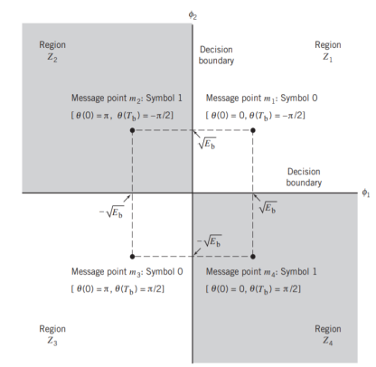
Fig 6: Signal-space diagram for MSK system
Generation and Coherent Detection of MSK Signals
With h = 1/2, we may use the block diagram of Figure(a) below to generate the MSK signal. The advantage of this method of generating MSK signals is that the signal coherence and deviation ratio are largely unaffected by variations in the input data rate. Two input sinusoidal waves, one of frequency fc = nc4Tb for some fixed integer nc and the other of frequency 14Tb, are first applied to a product modulator. This modulator produces two phase-coherent sinusoidal waves at frequencies f1 and f2, which are related to the carrier frequency fc and the bit rate 1/Tb in accordance with above equations for deviation ratio h = 12. These two sinusoidal waves are separated from each other by two narrowband filters, one centered at f1 and the other at f2. The resulting filter outputs are next linearly combined to produce the pair of quadrature carriers or orthonormal basis functions 1(t) and 2(t). Finally, 1(t) and 2(t) is multiplied with two binary waves a1(t) and a2(t), both of which have a bit rate equal to 1/(2Tb)


Fig 7: Block diagrams for (a) MSK transmitter and (b) coherent MSK receiver
Figure (b) above shows the block diagram of the coherent MSK receiver. The received signal x(t) is correlated with 1(t) and 2(t). In both cases, the integration interval is 2Tb seconds, and the integration in the quadrature channel is delayed by Tb seconds with respect to that in the in-phase channel. The resulting in-phase and quadrature channel correlator outputs, x1 and x2, are each compared with a threshold of zero
Error Probability of MSK
In the case of an AWGN channel, the received signal is given by
x(t) = s(t) + w(t)
Where s(t) is the transmitted MSK signal and w(t) is the sample function of a white Gaussian noise process of zero mean and power spectral density N0/2. To decide whether symbol 1 or symbol 0 was sent in the interval 0 t Tb, say, we have to establish a procedure for the use of x(t) to detect the phase states (0) and (Tb). For the optimum detection of (0), we project the received signal x(t) onto the reference signal over the interval –Tb t Tb, obtaining
x1 = 
w1 is the sample value of a Gaussian random variable of zero mean and variance N0/2. From the signal-space diagram, we see that if x1 > 0, the receiver chooses the estimate. On the other hand, if x1 0, it chooses the estimate. Similarly, for the optimum detection of (Tb), we project the received signal x(t) onto the second reference signal 2(t) over the interval 0 t 2Tb, obtaining
x2 =  0 ≤ t ≤ 2Tb
w2 is the sample value of another independent Gaussian random variable of zero mean and variance N02. Referring again to the signal space diagram, we see that if x2 0, the receiver chooses the estimate Tb= – 2. If, however, x2 0, the receiver chooses the estimate ˆ Tb = 2
It follows, therefore, that the BER for the coherent detection of MSK signals is given by
Pc = Q (2Eb/N0)
Key takeaway
- In M-ary PSK using coherent detection, increasing M improves the bandwidth efficiency, but the Eb/N0 required for the idealized condition of “error-free” transmission moves away from the Shannon limit as M is increased.
- In M-ary FSK, as the number of frequency-shift levels M is increased—which is equivalent to increased channel-bandwidth requirement—the operating point moves closer to the Shannon limit.
s(t) = A(t) cos(2πfct + θ(t) + θ)
A(t) = amplitude information
θ(t)= phase information
fc = the carrier frequency
θ = the phase shift introduced by the channel
- In coherent communications, θ is known to receivers
- In non-coherent communications, θ is unknown to receivers and assumed to be a random variable distributed uniformly over (-π, π)
- The phase shift is treated as a random variable distributed uniformly over (-π, π) and no phase estimation is provided at the receiver.
- We are now concerned with non-coherent communications
- The phase shift θ is the same during two consecutive signal transmission intervals
[(n-1)T, nT) and [nT, (n + 1)T).
- The information phase sequence {θn} is still differentially encoded as before.
- The transmitted signal s(t) in the interval [(n-1)T, (n +1)T] is

- θn = θn – θn-1 and θn-1 are independent. Both of them take values uniformly over
{0, 2π/M, . . ., 2π(M-1)/M}

Fig 8: DPSK generation
rn,c = Es cos(θn + θ) + ηn,c , rn,s = Es sin(θn + θ) + ηn,s
ηn,c, ηn,s , ηn-1, c , ηn-1, s are i.i.d
Each of them ~ N(0, N0/2)
Key Takeaways:
Here, the phase of the modulated signal is shifted relative to the previous signal element. No reference signal is considered here. The signal phase follows the high or low state of the previous element. This DPSK technique doesn’t need a reference oscillator.
When the digital symbol modulates amplitude, phase or frequency of the carrier without any reference to previous symbol, it is called memory less modulations.
PAM
In PAM, amplitude of pulses is varied in accordance with instantaneous value of modulating signal.

Fig 9. PAM waveform
PAM Generation:
The carrier which is in the form of narrow pulses has frequency fc. The uniform sampling takes place in multiplier to generate PAM signal. Samples are placed Ts sec away from each other.

Fig 10. PAM Modulator
- The circuit is simple emitter follower.
- In the absence of the clock signal, the output follows input.
- The modulating signal is applied as the input signal.
- Another input to the base of the transistor is the clock signal.
- The frequency of the clock signal is made equal to the desired carrier pulse train frequency.
- The amplitude of the clock signal is chosen the high level is at ground level(0v)
- Low level at some negative voltage sufficient to bring the transistor in cutoff region.
- When clock is high, circuit operates as emitter follower and the output follows in the input modulating signal.
- When clock signal is low, transistor is cutoff and output is zero.
- Thus the output is the desired PAM signal.
PAM Demodulator:
The PAM demodulator circuit which is just an envelope detector followed by a second order op-amp low pass filter (to have good filtering characteristics) is as shown below

Fig 11. PAM Demodulator
Key takeaway
The carrier which is in the form of narrow pulses has frequency fc. The uniform sampling takes place in multiplier to generate PAM signal. Samples are placed Ts sec away from each other.
PWM and PPM
There are two types of PTM systems. They are Pulse width modulation (PWM) and Pulse Position Modulation (PPM).
Pulse Width Modulation
In this type of modulation, the amplitude is maintained constant but the width of each pulse is varied in accordance with instantaneous value of the analog signal. In PWM information is contained in width variation. This is similar to FM. In pulse width modulation (PWM), the width of each pulse is made directly proportional to the amplitude of the information signal.
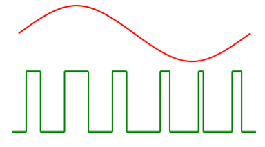
Fig 12. PWM waveform
PPM
In this type of modulation, the sampled waveform has fixed amplitude and width whereas the position of each pulse is varied as per instantaneous value of the analog signal. PPM signal is further modification of a PWM signal.
PPM and PWM modulator

Fig 13. PTM Modulator
- The PPM signal can be generated from PWM signal.
- The PWM pulses obtained at the comparator output are applied to a mono stable multi vibrator which is negative edge triggered.
- Hence for each trailing edge of PWM signal, the monostable output goes high. It remains high for a fixed time decided by its RC components.
- Thus as the trailing edges of the PWM signal keeps shifting in proportion with the modulating signal, the PPM pulses also keep shifting.
- Therefore all the PPM pulses have the same amplitude and width. The information is conveyed via changing position of pulses.

Fig 14. PWM and PPM Modulation waveforms.
PWM Demodulator

Fig 15. PWM Demodulator
- Transistor T1 works as an inverter.
- During time interval A-B when the PWM signal is high the input to transistor T2 is low.
- Therefore, during this time interval T2 is cut-off and capacitor C is charged through an R-C combination.
- During time interval B-C when PWM signal is low, the input to transistor T2 is high, and it gets saturated.
- The capacitor C discharges rapidly through T2.
- The collector voltage of T2 during BC is low.
- Thus, the waveform at the collector of T2is similar to saw-tooth waveform whose envelope is the modulating signal.
- Passing it through 2nd order op-amp Low Pass Filter, gives demodulated signal.
PPM Demodulator

Fig 16. PPM Demodulator
- The gaps between the pulses of a PPM signal contain the information regarding the modulating signal.
- During gap A-B between the pulses the transistor is cut-off and the capacitor C gets charged through R-C combination.
- During the pulse duration B-C the capacitor discharges through transistor and the collector voltage becomes low.
- Thus, waveform across collector is saw-tooth waveform whose envelope is the modulating signal.
- Passing it through 2nd order op-amp Low Pass Filter, gives demodulated signal.
Key takeaway
In pulse time modulation system, we use the increased bandwidth consumed by pulses to obtain an improvement in noise performance by representing the sample values of the message signal by some property of pulse rather than amplitude.
Comparison between PAM, PPM and PWM
SR. NO. | PARAMETER | PAM | PWM | PPM |
1 | Type of Carrier | Train of Pulses | Train of Pulses | Train of Pulses |
2 | Variable Characteristic of the Pulsed Carrier | Amplitude | Width | Position |
3 | Bandwidth Requirement | Low | High | High |
4 | Noise Immunity | Low | High | High |
5 | Information Contained in | Amplitude Variations | Width Variations | Position Variations |
6 | Transmitted Power | Varies with amplitude of pulses | Varies with variation in width | Remains Constant |
7 | Need to transmit synchronizing pulses | Not needed | Not needed | Necessary |
8 | Complexity of generation and detection | Complex | Easy | Complex |
9 | Similarity with other Modulation Systems | Similar to AM | Similar to FM | Similar to PM |
10 | Output waveforms | Refer Figure down | Refer Figure down | Refer Figure down |
QAM
QAM (also known as QASK) is a combination of ASK and PSK. Here, both the amplitude and the phase are varied to transmit more bits per symbol.
The QAM modulator essentially follows the idea that can be seen from the basic QAM theory where there are two carrier signals with a phase shift of 90° between them. These are then amplitude modulated with the two data streams known as the I or In-phase and the Q or quadrature data streams. These are generated in the baseband processing area.
Basic QAM I-Q modulator circuit
The two resultant signals are summed and then processed as required in the RF signal chain, typically converting them in frequency to the required final frequency and amplifying them as required.
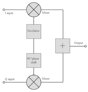
Fig.17: Basic QAM
It is worth noting that as the amplitude of the signal varies any RF amplifiers must be linear to preserve the integrity of the signal. Any non-linearities will alter the relative levels of the signals and alter the phase difference, thereby distorting he signal and introducing the possibility of data errors.
Basic QAM I-Q demodulator circuit
The basic modulator assumes that the two quadrature signals remain exactly in quadrature.
A further requirement is to derive a local oscillator signal for the demodulation that is exactly on the required frequency for the signal. Any frequency offset will be a change in the phase of the local oscillator signal with respect to the two double sideband suppressed carrier constituents of the overall signal.
Systems include circuitry for carrier recovery that often utilises a phase locked loop - some even have an inner and outer loop. Recovering the phase of the carrier is important otherwise the bit error rate for the data will be compromised.

Fig 18: Basic QAM demodulator
The circuits shown above show the generic IQ QAM modulator and demodulator circuits that are used in a vast number of different areas. Not only are these circuits made from discrete components, but more commonly they are used within integrated circuits that are able to provide a large number of functions.
Error Probability
BER for QAM constellation
The SER for a rectangular M-QAM (16-QAM, 64-QAM, 256-QAM etc) with size L = M2 can be calculated by considering two M-PAM on in-phase and quadrature components. The error probability of QAM symbol is obtained by the error probability of each branch (M-PAM) and is given by

Signal Space Representation
For the case when M = 2k , k even, the resulting signal space diagram has a “square constellation.” In this case the QAM signal can be thought of as 2 PAM signals in quadrature. For M = 2k, k odd, the constellation takes on a “cross” form. For example, 16-QAM constellation is

Fig 19:16-QAM constellation
Key takeaway
QAM (also known as QASK) is a combination of ASK and PSK. Here, both the amplitude and the phase are varied to transmit more bits per symbol.
Unit - 3
Digital Modulation Techniques
Unit - 3
Digital Modulation Techniques
(i) Generation
The QPSK Modulator uses a bit-splitter, two multipliers with local oscillator, a 2-bit serial to parallel converter, and a summer circuit.

Fig 1: QPSK generation
At the modulator’s input, the message signal’s even bits (i.e., 2nd bit, 4th bit, 6th bit, etc.) and odd bits (i.e., 1st bit, 3rd bit, 5th bit, etc.) are separated by the bits splitter and are multiplied with the same carrier to generate odd BPSK (called as PSKI) and even BPSK (called as PSKQ). The PSKQ signal is anyhow phase shifted by 90° before being modulated.
The QPSK waveform for two-bits input is as follows, which shows the modulated result for different instances of binary inputs.

(ii) Detection
The QPSK Demodulator uses two product demodulator circuits with local oscillator, two band pass filters, two integrator circuits, and a 2-bit parallel to serial converter.
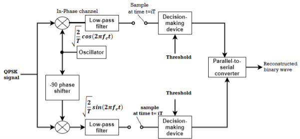
Fig 2: QPSK detectors
The two product detectors at the input of demodulator simultaneously demodulate the two BPSK signals. The pair of bits are recovered here from the original data. These signals after processing are passed to the parallel to serial converter.
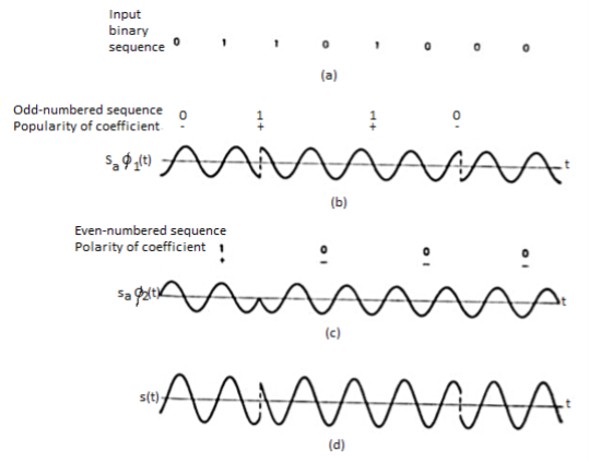
Fig 3: QPSK output
Error Calculation
In QPSK system the information carried by the transmitted signal is contained in the phase. The transmitted signals are given by


Where the carrier frequency fc=nc/7 for some fixed integer nc.
E = the transmitted signal energy per symbol.
T = Symbol duration.
The basic functions ɸ1(t) and ɸ2(t) are given by


There are four message points and the associated signal vectors are defined by

The table shows the elements of signal vectors, namely Si1 & Si2
Input dibit | Phase of QPSK signal (radians) | Coordinates of message points | Input dibit |
Si1 | Si2 | ||
10 | π/4 | +E/2 | -E/2 |
00 | 3π/2 | -E/2 | -E/2 |
01 | 5π/4 | +E/2 | +E/2 |
11 | 7π/4 | +E/2 | +E/2 |
Therefore, a QPSK signal is characterized by having a two-dimensional signal constellation (i.e., N=2) and four message points (i.e., M=4) as illustrated in figure.

Fig 4. Signal-space diagram of coherent QPSK system
A QPSK system is in fact equivalent to two coherent binary PSK systems working in parallel and using carriers that are in-phase and quadrature. The in-phase channel output x1 and the Q-channel output x2 may be viewed as the individual outputs of the two coherent binary PSK systems. Thus, the two binary PSK systems may be characterized as follows
The signal energy per bit √E/2
The noise spectral density is No/2
The average probability of bit error in each channel of the coherent QPSK system is 

The bit errors in the I-channel and Q-channel of the QPSK system are statistically independent. The I-channel makes a decision on one of the two bits constituting a symbol (di bit) of the QPSK signal and the Q-channel takes care of the other bit. Therefore, the average probability of a direct decision resulting from the combined action of the two channels working together is pc= probability of correct reception p1= probability of error


The average probability of symbol error for coherent QPSK is given by
Pe = 1 – PC = 
In the region where E/2No We may ignore the second term and so the approximate formula for the average probability of symbol error for coherent QPSK system is

Key takeaway
QPSK Modulator uses a bit-splitter, two multipliers with local oscillator, a 2-bit serial to parallel converter, and a summer circuit.
In the coherent detection of binary FSK signal, the phase information contained in the received signal is not fully exploited, other than to provide for synchronization of the receiver to the transmitter. We now show that by proper use of the continuous-phase property when performing detection, it is possible to improve the noise performance of the receiver significantly. Here again, this improvement is achieved at the expense of increased system complexity. Consider a continuous-phase frequency-shift keying (CPFSK) signal, which is defined for the signaling interval 0 t Tb as follows:
Where Eb is the transmitted signal energy per bit and Tb is the bit duration.
Another useful way of representing the CPFSK signal s(t) is to express it as a conventional angle-modulated signal:
s(t) =  cos [ 2πfct + θ(t)]
Where (t) is the phase of s(t) at time t. When the phase (t) is a continuous function of time, we find that the modulated signal s(t) is itself also continuous at all times, including the inter-bit switching times. The phase (t) of a CPFSK signal increases or decreases linearly with time during each bit duration of Tb seconds, as shown by
θ(t) = θ(0) ± (πh/Tb)t, 0 ≤ t ≤ Tb
Here the plus sign corresponds to sending symbol 1 and the minus sign corresponds to sending symbol 0; the dimensionless parameter h is to be defined. We deduce the following pair of relations:
fc + h/2TB = f1
fc – h/2TB = f2
Solving this pair of equations for fc and h, we get
fc = ½ (f1 + f2)
h – Tb (f1 – f2)
Signal-Space Diagram of MSK
Using a well-known trigonometric identity of conventional angle modulated signal, we may expand the CPFSK signal s(t) in terms of its in-phase and quadrature components as
s(t) =  cos θ (T) cos 2π fc t -
  sin θ (t) sin 2 π fct
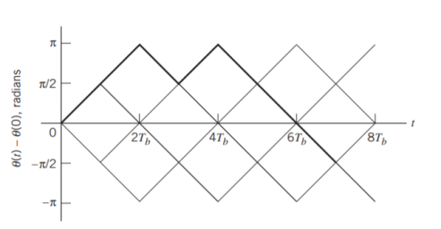
Fig 5: Boldfaced path represents the sequence 1101000.
Consider, first, the in-phase component √2Eb/Tbcos(t)
θ(t) = θ(0) ± π/2Tb, 0 ≤ t ≤ Tb
Where the plus sign corresponds to symbol 1 and the minus sign corresponds to symbol 0. A similar result holds for (t) in the interval –Tb t 0, except that the algebraic sign is not necessarily the same in both intervals. Since the phase (0) is 0 or depending on the past history of the modulation process, we find that in the interval –Tb t Tb, the polarity of cos(t) depends only on (0), regardless of the sequence of 1s and 0s transmitted before or after t = 0. Thus, for this time interval, the in-phase component consists of the half-cycle cosine pulse:
s1(t) =  cos θ (t)
=  cos θ (0) cos (πt/2Tb)
= ±  cos (πt/2Tb ) - Tb ≤ t ≤ Tb
Where the plus sign corresponds to (0) = 0 and the minus sign corresponds to (0) = . In a similar way, we may show that, in the interval 0 t 2Tb, the quadrature component of s(t) consists of the half-cycle sine pulse:
sQ(t) =  sin θ (t)
=  sin θ (Tb) sin (πt/2Tb)
= ±  sin (πt/2Tb ) 0 ≤ t ≤ 2Tb
Where the plus sign corresponds to (Tb) = 2 and the minus sign corresponds to (Tb)=–2. From the discussion just presented, we see that the in-phase and quadrature components of the MSK signal differ from each other in two important respects:
- They are in phase quadrature with respect to each other and
- The polarity of the in-phase component sI(t) depends on (0), whereas the polarity of the quadrature component sQ(t) depends on (Tb).
Moreover, since the phase states (0) and (Tb) can each assume only one of two possible values, any one of the following four possibilities can arise:
1. (0) = 0 and (Tb) = /2, which occur when sending symbol 1.
2. (0) = and (Tb) = /2, which occur when sending symbol 0.
3. (0) = and (Tb) = –/2 (or, equivalently, 3/2 modulo 2), which occur when sending symbol 1.
4. (0) = 0 and (Tb) = –/2, which occur when sending symbol 0.
This fourfold scenario, in turn, means that the MSK signal itself can assume one of four possible forms, depending on the values of the phase-state pair: (0) and (Tb).
Signal-Space Diagram
We see that there are two orthonormal basis functions 1(t) and 2(t) characterizing the generation of MSK; they are defined by the following pair of sinusoidally modulated quadrature carriers:
1(t) = 2/Tb cos (πt/2Tb) cos (2πfct) 0≤ t ≤ Tb
2(t) = 2/Tb sin (πt/2Tb) sin (2πfct) 0≤ t ≤ Tb
s(t) = s11(t) + s11(t) 0≤ t ≤ Tb
Where the coefficients s1 and s2 are related to the phase states (0) and (Tb), respectively. To evaluate s1, we integrate the product s(t)1(t) with respect to time t between the limits –Tb and Tb, obtaining
s1 = 
= Eb cos [θ(0)] -Tb ≤ t ≤ Tb
Similarly, to evaluate s2 we integrate the product s(t)2(t) with respect to time t between the limits 0 and 2Tb, obtaining
s2 = 
From above two equations we conclude that
1. Both integrals are evaluated for a time interval equal to twice the bit duration.
2. The lower and upper limits of the integral used to evaluate s1 are shifted by the bit duration Tb with respect to those used to evaluate s2.
3. The time interval 0 t Tb, for which the phase states (0) and (Tb) are defined, is common to both integrals.
It follows, therefore, that the signal constellation for an MSK signal is two-dimensional (i.e., N = 2), with four possible message points (i.e., M = 4), as illustrated in the signal space diagram of Figure below.
( + Eb , + Eb), ( - Eb , + Eb), ( - Eb , - Eb) and ( + Eb , - Eb)
The possible values of (0) and (Tb), corresponding to these four message points, are also included in Figure below. The signal-space diagram of MSK is thus similar to that of QPSK in that both of them have four message points in a two-dimensional space. However, they differ in a subtle way that should be carefully noted:
- QPSK, moving from one message point to an adjacent one, is produced by sending a two-bit symbol (i.e., dibit).
- MSK, on the other hand, moving from one message point to an adjacent one, is produced by sending a binary symbol, 0 or 1. However, each symbol shows up in two opposite quadrants, depending on the value of the phase-pair: (0) and (Tb).

Fig 6: Signal-space diagram for MSK system
Generation and Coherent Detection of MSK Signals
With h = 1/2, we may use the block diagram of Figure(a) below to generate the MSK signal. The advantage of this method of generating MSK signals is that the signal coherence and deviation ratio are largely unaffected by variations in the input data rate. Two input sinusoidal waves, one of frequency fc = nc4Tb for some fixed integer nc and the other of frequency 14Tb, are first applied to a product modulator. This modulator produces two phase-coherent sinusoidal waves at frequencies f1 and f2, which are related to the carrier frequency fc and the bit rate 1/Tb in accordance with above equations for deviation ratio h = 12. These two sinusoidal waves are separated from each other by two narrowband filters, one centered at f1 and the other at f2. The resulting filter outputs are next linearly combined to produce the pair of quadrature carriers or orthonormal basis functions 1(t) and 2(t). Finally, 1(t) and 2(t) is multiplied with two binary waves a1(t) and a2(t), both of which have a bit rate equal to 1/(2Tb)

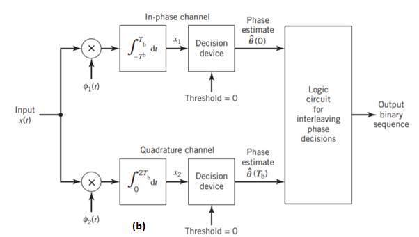
Fig 7: Block diagrams for (a) MSK transmitter and (b) coherent MSK receiver
Figure (b) above shows the block diagram of the coherent MSK receiver. The received signal x(t) is correlated with 1(t) and 2(t). In both cases, the integration interval is 2Tb seconds, and the integration in the quadrature channel is delayed by Tb seconds with respect to that in the in-phase channel. The resulting in-phase and quadrature channel correlator outputs, x1 and x2, are each compared with a threshold of zero
Error Probability of MSK
In the case of an AWGN channel, the received signal is given by
x(t) = s(t) + w(t)
Where s(t) is the transmitted MSK signal and w(t) is the sample function of a white Gaussian noise process of zero mean and power spectral density N0/2. To decide whether symbol 1 or symbol 0 was sent in the interval 0 t Tb, say, we have to establish a procedure for the use of x(t) to detect the phase states (0) and (Tb). For the optimum detection of (0), we project the received signal x(t) onto the reference signal over the interval –Tb t Tb, obtaining
x1 = 
w1 is the sample value of a Gaussian random variable of zero mean and variance N0/2. From the signal-space diagram, we see that if x1 > 0, the receiver chooses the estimate. On the other hand, if x1 0, it chooses the estimate. Similarly, for the optimum detection of (Tb), we project the received signal x(t) onto the second reference signal 2(t) over the interval 0 t 2Tb, obtaining
x2 =  0 ≤ t ≤ 2Tb
w2 is the sample value of another independent Gaussian random variable of zero mean and variance N02. Referring again to the signal space diagram, we see that if x2 0, the receiver chooses the estimate Tb= – 2. If, however, x2 0, the receiver chooses the estimate ˆ Tb = 2
It follows, therefore, that the BER for the coherent detection of MSK signals is given by
Pc = Q (2Eb/N0)
Key takeaway
- In M-ary PSK using coherent detection, increasing M improves the bandwidth efficiency, but the Eb/N0 required for the idealized condition of “error-free” transmission moves away from the Shannon limit as M is increased.
- In M-ary FSK, as the number of frequency-shift levels M is increased—which is equivalent to increased channel-bandwidth requirement—the operating point moves closer to the Shannon limit.
s(t) = A(t) cos(2πfct + θ(t) + θ)
A(t) = amplitude information
θ(t)= phase information
fc = the carrier frequency
θ = the phase shift introduced by the channel
- In coherent communications, θ is known to receivers
- In non-coherent communications, θ is unknown to receivers and assumed to be a random variable distributed uniformly over (-π, π)
- The phase shift is treated as a random variable distributed uniformly over (-π, π) and no phase estimation is provided at the receiver.
- We are now concerned with non-coherent communications
- The phase shift θ is the same during two consecutive signal transmission intervals
[(n-1)T, nT) and [nT, (n + 1)T).
- The information phase sequence {θn} is still differentially encoded as before.
- The transmitted signal s(t) in the interval [(n-1)T, (n +1)T] is

- θn = θn – θn-1 and θn-1 are independent. Both of them take values uniformly over
{0, 2π/M, . . ., 2π(M-1)/M}

Fig 8: DPSK generation
rn,c = Es cos(θn + θ) + ηn,c , rn,s = Es sin(θn + θ) + ηn,s
ηn,c, ηn,s , ηn-1, c , ηn-1, s are i.i.d
Each of them ~ N(0, N0/2)
Key Takeaways:
Here, the phase of the modulated signal is shifted relative to the previous signal element. No reference signal is considered here. The signal phase follows the high or low state of the previous element. This DPSK technique doesn’t need a reference oscillator.
When the digital symbol modulates amplitude, phase or frequency of the carrier without any reference to previous symbol, it is called memory less modulations.
PAM
In PAM, amplitude of pulses is varied in accordance with instantaneous value of modulating signal.
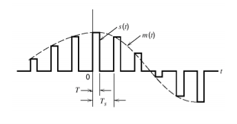
Fig 9. PAM waveform
PAM Generation:
The carrier which is in the form of narrow pulses has frequency fc. The uniform sampling takes place in multiplier to generate PAM signal. Samples are placed Ts sec away from each other.
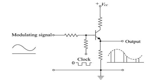
Fig 10. PAM Modulator
- The circuit is simple emitter follower.
- In the absence of the clock signal, the output follows input.
- The modulating signal is applied as the input signal.
- Another input to the base of the transistor is the clock signal.
- The frequency of the clock signal is made equal to the desired carrier pulse train frequency.
- The amplitude of the clock signal is chosen the high level is at ground level(0v)
- Low level at some negative voltage sufficient to bring the transistor in cutoff region.
- When clock is high, circuit operates as emitter follower and the output follows in the input modulating signal.
- When clock signal is low, transistor is cutoff and output is zero.
- Thus the output is the desired PAM signal.
PAM Demodulator:
The PAM demodulator circuit which is just an envelope detector followed by a second order op-amp low pass filter (to have good filtering characteristics) is as shown below
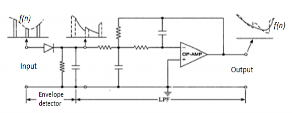
Fig 11. PAM Demodulator
Key takeaway
The carrier which is in the form of narrow pulses has frequency fc. The uniform sampling takes place in multiplier to generate PAM signal. Samples are placed Ts sec away from each other.
PWM and PPM
There are two types of PTM systems. They are Pulse width modulation (PWM) and Pulse Position Modulation (PPM).
Pulse Width Modulation
In this type of modulation, the amplitude is maintained constant but the width of each pulse is varied in accordance with instantaneous value of the analog signal. In PWM information is contained in width variation. This is similar to FM. In pulse width modulation (PWM), the width of each pulse is made directly proportional to the amplitude of the information signal.

Fig 12. PWM waveform
PPM
In this type of modulation, the sampled waveform has fixed amplitude and width whereas the position of each pulse is varied as per instantaneous value of the analog signal. PPM signal is further modification of a PWM signal.
PPM and PWM modulator

Fig 13. PTM Modulator
- The PPM signal can be generated from PWM signal.
- The PWM pulses obtained at the comparator output are applied to a mono stable multi vibrator which is negative edge triggered.
- Hence for each trailing edge of PWM signal, the monostable output goes high. It remains high for a fixed time decided by its RC components.
- Thus as the trailing edges of the PWM signal keeps shifting in proportion with the modulating signal, the PPM pulses also keep shifting.
- Therefore all the PPM pulses have the same amplitude and width. The information is conveyed via changing position of pulses.
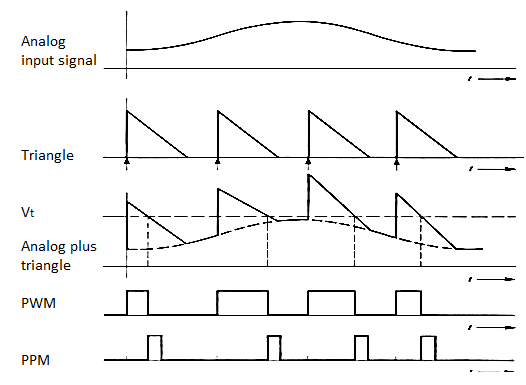
Fig 14. PWM and PPM Modulation waveforms.
PWM Demodulator
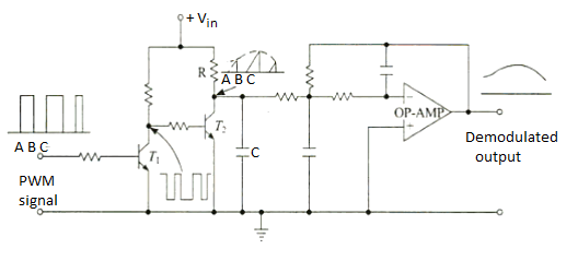
Fig 15. PWM Demodulator
- Transistor T1 works as an inverter.
- During time interval A-B when the PWM signal is high the input to transistor T2 is low.
- Therefore, during this time interval T2 is cut-off and capacitor C is charged through an R-C combination.
- During time interval B-C when PWM signal is low, the input to transistor T2 is high, and it gets saturated.
- The capacitor C discharges rapidly through T2.
- The collector voltage of T2 during BC is low.
- Thus, the waveform at the collector of T2is similar to saw-tooth waveform whose envelope is the modulating signal.
- Passing it through 2nd order op-amp Low Pass Filter, gives demodulated signal.
PPM Demodulator

Fig 16. PPM Demodulator
- The gaps between the pulses of a PPM signal contain the information regarding the modulating signal.
- During gap A-B between the pulses the transistor is cut-off and the capacitor C gets charged through R-C combination.
- During the pulse duration B-C the capacitor discharges through transistor and the collector voltage becomes low.
- Thus, waveform across collector is saw-tooth waveform whose envelope is the modulating signal.
- Passing it through 2nd order op-amp Low Pass Filter, gives demodulated signal.
Key takeaway
In pulse time modulation system, we use the increased bandwidth consumed by pulses to obtain an improvement in noise performance by representing the sample values of the message signal by some property of pulse rather than amplitude.
Comparison between PAM, PPM and PWM
SR. NO. | PARAMETER | PAM | PWM | PPM |
1 | Type of Carrier | Train of Pulses | Train of Pulses | Train of Pulses |
2 | Variable Characteristic of the Pulsed Carrier | Amplitude | Width | Position |
3 | Bandwidth Requirement | Low | High | High |
4 | Noise Immunity | Low | High | High |
5 | Information Contained in | Amplitude Variations | Width Variations | Position Variations |
6 | Transmitted Power | Varies with amplitude of pulses | Varies with variation in width | Remains Constant |
7 | Need to transmit synchronizing pulses | Not needed | Not needed | Necessary |
8 | Complexity of generation and detection | Complex | Easy | Complex |
9 | Similarity with other Modulation Systems | Similar to AM | Similar to FM | Similar to PM |
10 | Output waveforms | Refer Figure down | Refer Figure down | Refer Figure down |
QAM
QAM (also known as QASK) is a combination of ASK and PSK. Here, both the amplitude and the phase are varied to transmit more bits per symbol.
The QAM modulator essentially follows the idea that can be seen from the basic QAM theory where there are two carrier signals with a phase shift of 90° between them. These are then amplitude modulated with the two data streams known as the I or In-phase and the Q or quadrature data streams. These are generated in the baseband processing area.
Basic QAM I-Q modulator circuit
The two resultant signals are summed and then processed as required in the RF signal chain, typically converting them in frequency to the required final frequency and amplifying them as required.

Fig.17: Basic QAM
It is worth noting that as the amplitude of the signal varies any RF amplifiers must be linear to preserve the integrity of the signal. Any non-linearities will alter the relative levels of the signals and alter the phase difference, thereby distorting he signal and introducing the possibility of data errors.
Basic QAM I-Q demodulator circuit
The basic modulator assumes that the two quadrature signals remain exactly in quadrature.
A further requirement is to derive a local oscillator signal for the demodulation that is exactly on the required frequency for the signal. Any frequency offset will be a change in the phase of the local oscillator signal with respect to the two double sideband suppressed carrier constituents of the overall signal.
Systems include circuitry for carrier recovery that often utilises a phase locked loop - some even have an inner and outer loop. Recovering the phase of the carrier is important otherwise the bit error rate for the data will be compromised.

Fig 18: Basic QAM demodulator
The circuits shown above show the generic IQ QAM modulator and demodulator circuits that are used in a vast number of different areas. Not only are these circuits made from discrete components, but more commonly they are used within integrated circuits that are able to provide a large number of functions.
Error Probability
BER for QAM constellation
The SER for a rectangular M-QAM (16-QAM, 64-QAM, 256-QAM etc) with size L = M2 can be calculated by considering two M-PAM on in-phase and quadrature components. The error probability of QAM symbol is obtained by the error probability of each branch (M-PAM) and is given by

Signal Space Representation
For the case when M = 2k , k even, the resulting signal space diagram has a “square constellation.” In this case the QAM signal can be thought of as 2 PAM signals in quadrature. For M = 2k, k odd, the constellation takes on a “cross” form. For example, 16-QAM constellation is
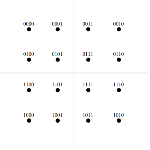
Fig 19:16-QAM constellation
Key takeaway
QAM (also known as QASK) is a combination of ASK and PSK. Here, both the amplitude and the phase are varied to transmit more bits per symbol.
GENERATION AND COHERENT DETECTION OF BPSK SIGNALS
(i) Generation
To generate the BPSK signal, we build on the fact that the BPSK signal is a special case of DSB-SC modulation. Specifically, we use a product modulator consisting of two components.
(i) Non-return-to-zero level encoder, whereby the input binary data sequence is encoded inpolar form with symbols 1 and 0 represented by the constant-amplitude.
(ii) Product modulator, which multiplies the level encoded binary wave by the sinusoidal carrier of amplitude to produce the BPSK signal. The timing pulses used to generate the level encoded binary wave and the sinusoidal carrier wave are usually, but not necessarily, extracted from a common master clock.

(ii) Detection
To detect the original binary sequence of 1s and 0s, the BPSK signal at the channel output is applied to a receiver that consists of four sections
(a)Product modulator, which is also supplied with a locally generated reference signal thatis a replica of the carrier wave
(b)Low-pass filter, designed to remove the double-frequency components of the product modulator output (i.e., the components centered on) and pass the zero-frequency components.
(c)Sampler, which uniformly samples the output of the low-pass filter at where; the localclock governing the operation of the sampler issynchronized with the clock responsible for bit-timing in the transmitter.
(d)Decision-making device, which compares the sampled value of the low-pass filtersoutput to an externally supplied threshold, every seconds. If the threshold is exceeded, the device decides in favor of symbol 1; otherwise, it decides in favor of symbol 0. Levels.
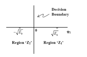
The signal B is


QPSK
For Gray encoding,  can directly be computed.
Assume that  is transmitted which corresponds to
  Then the conditional bit error probability is given by


From the direct decision rule for data bits

 2=1⇔Y∈D2⋃D3
Thus,


By symmetry all conditional four bit errors probabilities are identical. Since two data bits are transmitted per modulation symbol (waveform) in QPSK, we have the relations  and .Therefore,


Offset Quadriphase-Shift Keying
QPSK : carrier phase may jump by ± 90° or ± 180° every 2 bit durations Problem : filtering action can cause the carrier amplitude to fluctuate → receiver produce additional symbol errors To reduce fluctuation → Offset Quadriphase-Shift Keying
Second substream m2 (t) is delayed (offset) by a bit duration T
Phase transitions are confined in 0°, ± 90°
π/4-Shifted Quadriphase-Shift Keying
Similar to Offset Quadriphase-Shift Keying (OQPSK) Carrier phase of QPSK can be (usually 1.):
1. 0, π/2, π or 3π/2
2. π/4, 3π/4, 5π/4 or 7π/4
The amplitude fluctuations during filtering are significantly reduced
• Reduced amplitude fluctuation becomes important when transmitter includes slightly nonlinear amplifier.
π/4-Shifted QPSK has been adopted in north American digital cellular time division multiple access (TDMA) standard IS-54 as well as the Japanese digital cellular standard.
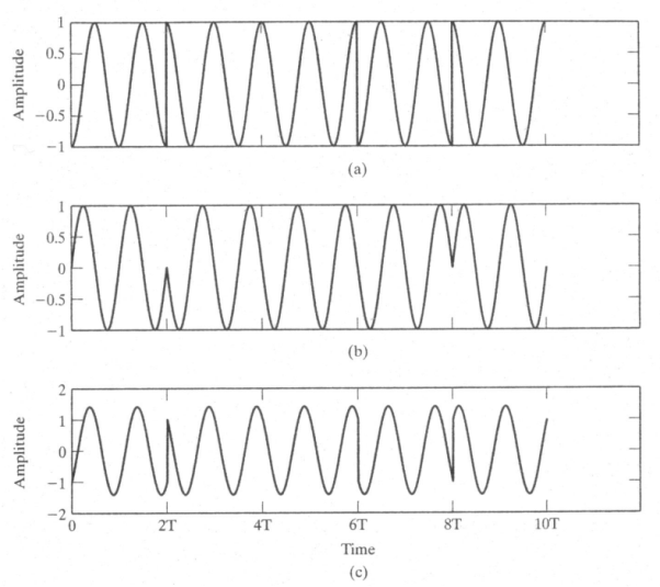
CPFSK
In rectangular pulse shaping (Linear Pulse Shaping), phase changes linearly with the time, and the frequency is held constant throughout the data interval. In general, frequency pulse of length L is denoted by LREC. With L = 1, 1REC-CPM signal is called Continuous Phase Frequency Shift Keying (CPFSK). Note that although the rectangular pulse-shaping function is discontinuous, the phase response function is continuous. Frequency function f(t), of linear pulse shape with full response CPM (L = 1) signaling is given as:

And the corresponding phase function

So, for full response CPFSK,
(t, a)= aig(t – (i – 1)T) +θi, (i-1)T ≤ t ≤ iT,
θ(t, ai) = aig(t – (i – 1)T) = πhai(t – (i – 1)T)/T, (i – 1)T ≤ t ≤ iT
θi = πh  (i – 1)T ≤ t ≤ iT
In order to better understand CPFSK signals, we provide the following plots. Figure shows the phase state plot for 2-CPFSK with. It can be inferred from the Figure that the transmitted sequence is, based on the direction the signal moves in, or the slope of the signal within the bit interval. Figure shows the physical phase state, which is the observed phase. The jumps in the physical phase state are not discontinuities. They are the phase state but wrapped within the interval. Figures amplitudes are the normalized phase with respect to. No discontinuities are present due to the inherent memory characteristics of CPM signals. Figure shows the passband CPFSK signal. It can be noticed how frequency changes based on the data input, increasing with a +1 input and decreasing with -1 input. Moreover, the frequency change is noticed to be instantaneous at the beginning of each interval and holds its value for the rest of the bit interval


Figures above show the phase tree and phase trellis for 2-CPFSK and h= 1/2, respectively. We emphasize that the phase transitions in the state trellis diagram in Figure shows from one state to another are not true phase trajectories. They represent phase transitions for the terminal/observed states at the time instants t= (i-1)T, 1 i
i n.
n.
CPM
Continuous Phase Modulation (CPM) is a memory-type, constant-envelope, nonlinear modulation, which allows the use of power efficient low cost, nonlinear power amplifiers without introducing distortion. Digital transmission using constant-envelope CPM has become important because of its attractive properties. The constant-envelope designs are fairly immune to nonlinear channel effects. Although constructions of CPM are diverse in their properties and applications, they all rely upon the use of inherent memory introduced by the continuous phase. This constraint of continuous phase not only provides faster spectral roll-off, but also permits multiple symbol detection rather than the more conventional symbol-by-symbol detection. In this Chapter, two subclasses of CPM called Continuous Phase Frequency Shift Keying (CPFSK) and Continuous Phase Chirp Keying (CPCK) are described, although the treatment provided applies, in general, to any CPM. Concepts, mathematical descriptions and properties of CPM signals are presented with primary focus on CPFSK and CPCK signaling techniques.
The general form of a CPM signal is given by
s(t, a) = 2Eb/T cos(2πfct + (t, a) + 0), 0≤t≤nπ,
Where is the symbol energy, is the symbol duration, is the carrier frequency, is the initial phase offset which is assumed to be zero for coherent detection without any loss of generality. Is a sequence of independent and identically distributed M-ary information symbols each taking one of the  values with an equal probability of 1/M such that,
a = (a1, a2, . . . , an), ak ∈ { ±1, ±3, . . . , ±(M-1)}, 1≤k≤n,
Where and the phase function is defined as the integral of an instantaneous frequency pulse and is given by:
(t, a) =  (i – 1)T≤ t ≤iT,
g(t) = 2 π 
The derivative of g(t) is the frequency pulse shape f(t). That is

Where L is the frequency response pulse length. The frequency pulse length dictates the time interval over which a single input data symbol can affect the instantaneous frequency. Depending on the value of L, two different schemes of CPM can be defined. When L=1, the entire pulse extends over one full symbol interval. This type of CPM is known as full response CPM. When L>1, only a part of the pulse shape extends over a symbol and is known as partial response CPM signaling.
Generation of CPM

Data sequence passes through the pulse shaping filter and the multiplier to form frequency pulse sequence, which is then FM modulated to generate the CPM signal.
The phase of CPM can be represented by a tree structure. The tree structure is found by manipulating the information carrying phase. It can be viewed as the sum of two phase terms: instantaneous phase and accumulated phase. The phase of CPM signal during the ith symbol interval to give
(t, a) = 
= θ(t, ai) + θi (i – 1)T≤ t ≤iT,
θ(t, ai) = 
Which represents the changing part of the total phase during (i-1) T t
t iT and is determined by the current data symbols and previous L-1 symbols. The first term of Equation above, is dependent on the sequence of past input data symbols and the current data input (ai-L+1,….., ai-1) , and is called the correlative state. There are M L-1 possible correlative states. Since we are only interested in full response CPM , then
θ(t, ai) = aig(t – (i-1)T), (i – 1)T≤ t ≤iT
And is the accumulated phase, the phase state, which represents the constant part of the total phase in the same interval is
θi = g(t = T)  (i – 1)T≤ t ≤iT
The accumulated phase can be interpreted as the sum of the maximum phase changes contributed by each symbol, accumulated along the time axis up to the (i-1) symbol interval. It can be computed recursively as
θi+1 = θi + g(t = T)ai
The phase behavior of CPM signals can be best described by sketching the set of phase trajectories ɸ(t,a) generated by all possible values of the information sequence {ai} . These phase diagrams are called phase trees and they are specific to each CPM scheme, based on the different modulation parameters, the M-ary points and most importantly the phase function g(t).
References:
1. Lathi B.P. - Modern Digital and Analog communications systems - PRISM Indian Ed.
2. Digital Communication: J.S.Chitode
3. Digital Communication (Fundamentals & applications): Bernard Scalr
4. Introduction to Error Control Codes: Salvatore Gravano
5. OFDM For wireless communication systems: Ramjee Prasad
6. Modern Communication systems (Principles and application): Leon W. Couch II (PHI)
7. Error Control Coding: Shu Lin & Daniel J.Costello