UNIT 3
Number System And Logic Gates
3.1 Number System and conversion
Introduction to number system and conversions
A digital system understands positional number system where there are few symbols called digits and these symbol represents different values depending on their position in the number.
A value of the digit is determined by using
- The digit
- Its position
- The base of the number system
Decimal Number System
- Its the system that we use in our daily life. It has a base 10 and uses 10 digits from 0 to 9.
- Here, the successive positions towards the left of the decimal point represent units, tens, hundreds, thousands and so on.
- Each and every position represents a specific power of the base (10). For example, the decimal number 4321 consists of the digit 1 in the units position, 2 in the tens position, 3 in the hundreds position, and 4 in the thousands position, and its value can be written as
(1×1000) + (2×100) + (3×10) + (4×l)
(1×10³) + (2×10²) + (3×101) + (4×l00)
1000 + 200 + 30 + 1
1234
- As a computer programmer, we should understand the following number systems used in computers.
S.N. | Number System & Description |
1 | Binary Number System Base 2. Digits used: 0 and 1 |
2 | Octal Number System Base 8. Digits used: 0 to 7 |
3 | Hexa Decimal Number System Base 16. Digits used: 0 to 9, Letters used: A- F |
3.2 Binary their conversion
- It uses two digits 0 and 1.
- It is also called as base 2 number system.
- Here, each position in any binary number represents a power of the base (2). Example: 23
- The last position represents a y power of the base (2). Example: 2y where y represents the last position.
Example
Binary Number: 101112
Calculating the Decimal Equivalent of binary number −
Step | Binary Number | Decimal Number |
Step 1 | 101012 | ((1 × 24) + (0 × 23) + (1 × 22) + (1 × 21) + (1 × 20))10 |
Step 2 | 101012 | (16 + 0 + 4 + 2 + 1)10 |
Step 3 | 101012 | 2310 |
Note: 101112 is normally written as 10111.
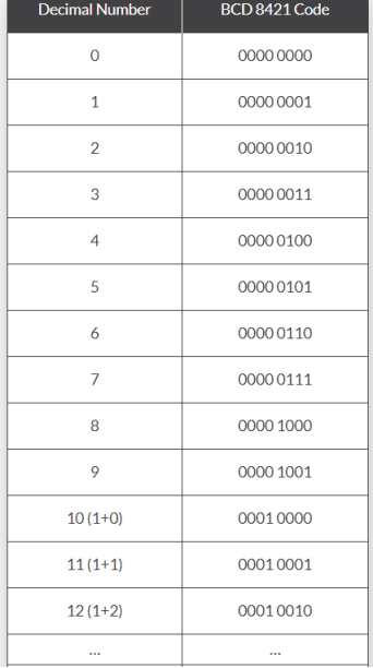
3.3 BCD their conversion
BCD numbers are from 0 to 9.
3.4 Octal Number System
- It consists of eight digits 0, 1,2,3,4,5,6,7.
- It is also named as base 8 number system.
- Here each position represents a power of the base (8). Example: 82
- The last position represents a y power of the base (8). Example: 8y where y represents the last position .
Example
Octal Number − 125758
Calculating Decimal Equivalent −
Step | Octal Number | Decimal Number |
Step 1 | 125758 | ((1 × 84) + (2 × 83) + (5 × 82) + (7 × 81) + (5 × 80))10 |
Step 2 | 125758 | (4096 + 1024 + 320 + 56 + 5)10 |
Step 3 | 125758 | 550010 |
Note: 125758 is normally written as 12575 in octal.
3.5 Decimal to Any Base System
It includes the following steps:
- Firstly, divide the decimal number which is to be converted by the value of its new base.
- Then, after getting the remainder from the above step make it the rightmost digit (least significant digit) i.e. LSD of new base number.
- Further divide the quotient by the new base.
- Then record the remainder from the above step as the next digit (towards the left) of the new base number.
- Repeat these steps and get remainders from right to left till the quotient becomes zero.
- The last remainder obtained will be the Most Significant Digit (MSD) of the new base number.
For example −
Decimal Number: 2710
Calculating Binary Equivalent −
Step | Operation | Result | Remainder |
Step 1 | 27 / 2 | 13 | 1 |
Step 2 | 13 / 2 | 6 | 1 |
Step 3 | 6 / 2 | 3 | 0 |
Step 4 | 3 / 2 | 1 | 1 |
Step 5 | 1 / 2 | 0 | 1 |
Hence, the remainders are arranged in the reverse order and we get:
Decimal Number − 2710 = Binary Number − 110112.
3.6 Hexadecimal Number System
- It uses 10 digits starting from 0,1,2,3,4,5,6,7,8,9 and 6 letters A,B,C,D,E,F.
- These letters represents numbers as A = 10, B = 11, C = 12, D = 13, E = 14, F = 15.
- It is also known as base 16 number system.
- Here each position represents a power of the base (16). Example 161.
- The last position represents a y power of the base (16). Example: 16y where y represents the last position .
Example −
Hexadecimal Number: 19FDA16
Calculating Decimal Equivalent −
Step | Hexadecimal Number | Decimal Number |
Step 1 | 19FDA16 | ((1 × 164) + (9 × 163) + (F × 162) + (D × 161) + (A × 160))10 |
Step 2 | 19FDA16 | ((1 × 164) + (9 × 163) + (15 × 162) + (13 × 161) + (10 × 160))10 |
Step 3 | 19FDA16 | (65536 + 36864 + 3840 + 208 + 10)10 |
Step 4 | 19FDA16 | 10645810 |
Note − 19FDA16 is normally written as 19FDA in hexa decimal.
Conversions
There are many techniques which are used to convert numbers from one base to another. These are as follows −
- Decimal to any other Base System
- Any Base System to Decimal
- Any Base System to Non-Decimal
- Binary to Octal
- Octal to Binary
- Binary to Hexadecimal
- Hexadecimal to Binary
Any Base System to Decimal System
- Here, the column (positional) value of each digit (this depends on the position of the digit and the base of the number system) is multiplied with the obtained column values of the digits in the corresponding columns.
- The sum the products is then calculated which gives the total equivalent value in decimal.
For example :
Binary Number − 111102
Calculating Decimal Equivalent −
Step | Binary Number | Decimal Number |
Step 1 | 111102 | ((1 × 24) + (1 × 23) + (1 × 22) + (1 × 21) + (0 × 20))10 |
Step 2 | 111102 | (16 + 8 + 4 + 2 + 0)10 |
Step 3 | 111102 | 3010 |
Binary Number − 111102 = Decimal Number − 3010
Any Base System to Non-Decimal System
- The original number is converted to its equivalent decimal number (base 10).
- Then the decimal number so obtained is further converted to the new base number.
Example
Octal Number − 268
Calculating its Binary Equivalent −
Step 1 – Converting octal to Decimal
Step | Octal Number | Decimal Number |
Step 1 | 268 | ((2 × 81) + (6 × 80))10 |
Step 2 | 268 | (16 + 6 )10 |
Step 3 | 268 | 2210 |
Octal Number − 268 = Decimal Number − 2210
Step 2 − Converting Decimal to Binary
Step | Operation | Result | Remainder |
Step 1 | 22 / 2 | 11 | 0 |
Step 2 | 11 / 2 | 5 | 1 |
Step 3 | 5 / 2 | 2 | 1 |
Step 4 | 2 / 2 | 1 | 0 |
Step 5 | 1 / 2 | 0 | 1 |
Decimal Number − 2210 = Binary Number − 101102
Octal Number − 268 = Binary Number − 101102
Binary to Octal
- Dividing the binary digits into groups of three starting from right to left.
- Converting each group of three binary digits into one octal digit.
For example:
Binary Number − 101012
Its Octal Equivalent −
Step | Binary Number | Octal Number |
Step 1 | 101012 | 010 101 |
Step 2 | 101012 | 28 58 |
Step 3 | 101012 | 258 |
Binary Number − 101012 = Octal Number − 258
Octal to Binary
- Converting each octal digit to a 3 digit binary number and they can be treated as decimal number for this conversion.
- Then combining all the resulting binary groups into a single binary number.
For example:
Octal Number − 258
Its Binary Equivalent −
Step | Octal Number | Binary Number |
Step 1 | 258 | 210 510 |
Step 2 | 258 | 0102 1012 |
Step 3 | 258 | 0101012 |
Octal Number − 258 = Binary Number − 101012
Binary to Hexadecimal
- Dividing the binary digits into groups of four (starting from right to left).
- Then converting each group of four binary digits into one hexadecimal number.
For example:
Binary Number − 101012
Its hexadecimal Equivalent −
Step | Binary Number | Hexadecimal Number |
Step 1 | 101012 | 0001 0101 |
Step 2 | 101012 | 110 510 |
Step 3 | 101012 | 1516 |
Binary Number − 101012 = Hexadecimal Number − 1516
Hexadecimal to Binary
- Converting each hexadecimal digit to a 4 digit binary number and they can be treated as decimal number.
- Combining all the resulting binary groups into a single binary number.
For example:
Hexadecimal Number − 1516
Its Binary Equivalent −
Step | Hexadecimal Number | Binary Number |
Step 1 | 1516 | 110 510 |
Step 2 | 1516 | 00012 01012 |
Step 3 | 1516 | 000101012 |
Hexadecimal Number − 1516 = Binary Number − 101012
It is an essential part of all the digital calculations.
Binary Addition
- It is a basis for binary subtraction, multiplication, division.
- There are four rules which are as follows:
|
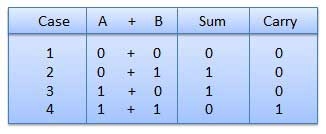
Fig.1 Rules of Binary addition
In fourth step, a sum (1 + 1 = 10) i.e. 0 is written in the given column and a carry of 1 over to the next column is done.
For Example −
|
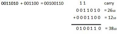
Fig.2 Binary addition
Binary Subtraction
Subtraction and Borrow, these are the two words that will be used very frequently for binary subtraction. There rules of binary subtraction are:
|
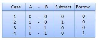
Fig.3 Rules of Binary Subtraction
For Example
|
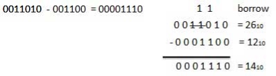
Fig.4 Binary subtraction
Binary Multiplication
- It is similar to decimal multiplication.
- It is also simpler than decimal multiplication as only 0s and 1s are involved.
- There are four rules of binary multiplication which are:
|
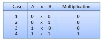
Fig.5 Rules of Binary Multiplication (Ref. 1)
For Example
|
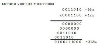
Fig.6 Binary Multiplication
Binary Division
- It is similar to decimal division.
- It is also called as the long division procedure.
For Example
|
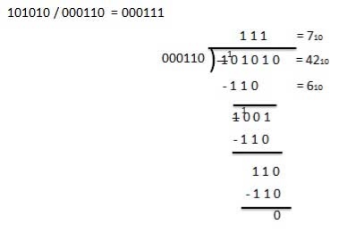
Fig.7 Binary Division
Binary system complements
- Complements are used in order to simplify the subtraction operation and the logical manipulations can be done.
- For each radix-r system there are two types of complements:
S.N. | Complement | Description |
1 | Radix Complement | It is referred to as the r's complement. |
2 | Diminished Radix Complement | It is referred to as the (r-1)'s complement. |
- The binary system has radix r = 2.
- Therefore, the two types of complements for the binary system are known as 1's complement and 2's complement.
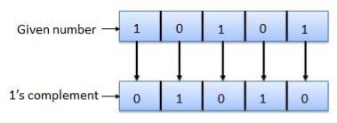
1's complement
Fig.8: 1's complement
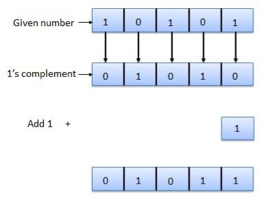
2's complement
Fig.9: 2's complement
|
Octal Number System
- It consists of eight digits 0, 1,2,3,4,5,6,7.
- It is also named as base 8 number system.
- Here each position represents a power of the base (8). Example: 82
- The last position represents a y power of the base (8). Example: 8y where y represents the last position .
Example
Octal Number − 125758
Calculating Decimal Equivalent −
Step | Octal Number | Decimal Number |
Step 1 | 125758 | ((1 × 84) + (2 × 83) + (5 × 82) + (7 × 81) + (5 × 80))10 |
Step 2 | 125758 | (4096 + 1024 + 320 + 56 + 5)10 |
Step 3 | 125758 | 550010 |
Note: 125758 is normally written as 12575 in octal.
Octal Addition
The octal addition table is as follows:
|
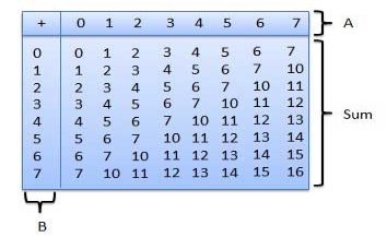
Fig.10: Octal addition table
- To use the above table, simply follow the example:
- Add 68and 58.
- Locate 6 in the A column then locate the 5 in the B column.
- The point in 'sum' area where these two columns intersect is the 'sum' of two numbers.
68 + 58 = 138.
For Example :
|
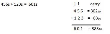
Fig.11: Octal addition (Ref. 1)
Octal Subtraction
- It follows the same rules as the subtraction of numbers in any other system.
- The only difference is in borrowed number.
- In the decimal system, we borrow a group of 1010.
- In the binary system, we borrow a group of 210.
- But in the octal system we borrow a group of 810.
For Example
|
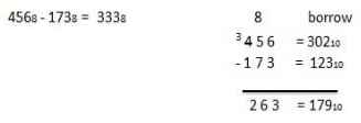
Fig.12: Octal subtraction (Ref. 1)
3.8 De Morgan’s Theorem
- It is useful in finding the complement of Boolean function.
- It states that “The complement of logical OR of at least two Boolean variables is equal to the logical AND of each complemented variable”.
- It can be represented using 2 Boolean variables x and y as
(x + y)’ = x’.y’
- The dual of the above Boolean function is
(x.y)’ = x’ + y’
- Therefore, the complement of logical AND of the two Boolean variables is equivalent to the logical OR of each complemented variable.
- Similarly, DeMorgan’s theorem can be applied for more than 2 Boolean variables also.
Simplification of Boolean Functions
Numerical
- Simplify the Boolean function,
f = p’qr + pq’r + pqr’ + pqr
Method 1 Given f = p’qr + pq’r + pqr’ +pqr. In first and second term r is common and in third and fourth terms pq is common. So, taking out the common terms by using Distributive law we get, ⇒ f = (p’q + pq’)r + pq(r’ + r) The terms present in first parenthesis can be simplified by using Ex-OR operation. The terms present in second parenthesis is equal to ‘1’ using Boolean postulate we get ⇒ f = (p ⊕q)r + pq(1) The first term can’t be simplified further. But, the second term is equal to pq using Boolean postulate. ⇒ f = (p ⊕q)r + pq Therefore, the simplified Boolean function is f = (p⊕q)r + pq
Method 2 Given f = p’qr + pq’r + pqr’ + pqr. Using the Boolean postulate, x + x = x. Hence we can write the last term pqr two more times. ⇒ f = p’qr + pq’r + pqr’ + pqr + pqr + pqr Now using the Distributive law for 1st and 4th terms, 2nd and 5th terms, 3rdand 6th terms we get. ⇒ f = qr(p’ + p) + pr(q’ + q) + pq(r’ + r) Using Boolean postulate, x + x’ = 1 and x.1 = x for further simplification . ⇒ f = qr(1) + pr(1) + pq(1) ⇒ f = qr + pr + pq ⇒ f = pq + qr + pr Therefore, the simplified Boolean function is f = pq + qr + pr. Hence we got two different Boolean functions after simplification of the given Boolean function. Functionally, these two functions are same. As per requirement, we can choose one of them.
|
Numerical
Find the complement of the Boolean function,
f = p’q + pq’.
Solution:
Using DeMorgan’s theorem, (x + y)’ = x’.y’ we get
⇒ f’ = (p’q)’.(pq’)’
Then by second law, (x.y)’ = x’ + y’ we get
⇒ f’ = {(p’)’ + q’}.{p’ + (q’)’}
Then by using, (x’)’=x we get
⇒ f’ = {p + q’}.{p’ + q}
⇒ f’ = pp’ + pq + p’q’ + qq’
Using x.x’=0 we get
⇒ f = 0 + pq + p’q’ + 0
⇒ f = pq + p’q’
Therefore, the complement of Boolean function, p’q + pq’ is pq + p’q’.
LOGIC GATES
The basic gates are namely AND gate, OR gate & NOT gate.
3.9 AND gate
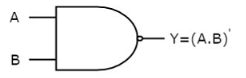
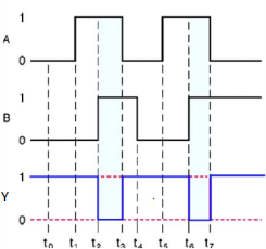
It is a digital circuit that consists of two or more inputs and a single output which is the logical AND of all those inputs. It is represented with the symbol ‘.’.
The following is the truth table of 2-input AND gate.
A | B | Y = A.B |
0 | 0 | 0 |
0 | 1 | 0 |
1 | 0 | 0 |
1 | 1 | 1 |
Here A, B are the inputs and Y is the output of two input AND gate.
If both inputs are ‘1’, then only the output, Y is ‘1’. For remaining combinations of inputs, the output, Y is ‘0’.
The figure below shows the symbol of an AND gate, which is having two inputs A, B and one output, Y.
Fig. : AND gate (ref. 1)
Timing Diagram:
|

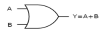
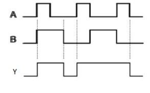
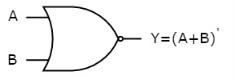
3.10 OR gate
It is a digital circuit which has two or more inputs and a single output which is the logical OR of all those inputs. It is represented with the symbol ‘+’. The truth table of 2-input OR gate is:
Here A, B are the inputs and Y is the output of two input OR gate. When both inputs are ‘0’, then only the output, Y is ‘0’. For remaining combinations of inputs, the output, Y is ‘1’. The figure below shows the symbol of an OR gate, which is having two inputs A, B and one output, Y. Fig. : OR gate (ref. 1)
Timing Diagram: |
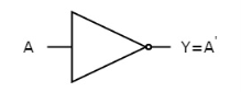
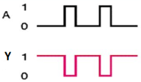
3.11 NOT gate
It is a digital circuit that has one input and one output. Here the output is the logical inversion of input. Hence, it is also called as an inverter. The truth table of NOT gate is:
Here A and Y are the corresponding input and output of NOT gate. When A is ‘0’, then, Y is ‘1’. Similarly, when, A is ‘1’, then, Y is ‘0’. The figure below shows the symbol of NOT gate, which has one input, A and one output, Y. Fig. : NOT gate (ref. 1)
Timing Diagram:
|
Universal gates
- NAND & NOR gates are known as universal gates.
- We can implement any Boolean function by using NAND gates and NOR gates alone.
NAND gate
It is a digital circuit which has two or more inputs and single output and it is the inversion of logical AND gate. The truth table of 2-input NAND gate is:
Here A, B are the inputs and Y is the output of two input NAND gate. When both inputs are ‘1’, then the output, Y is ‘0’. If at least one of the input is zero, then the output, Y is ‘1’. This is just the inverse of AND operation. The image shows the symbol of NAND gate: Fig.: NAND gate (ref. 1)
NAND gate works same as AND gate followed by an inverter. Timing Diagram:
|
NOR gate
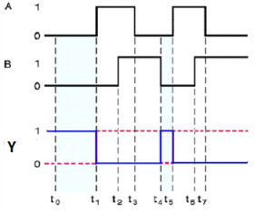
It is a digital circuit that has two or more inputs and a single output which is the inversion of logical OR of all inputs. The truth table of 2-input NOR gate is:
Here A and B are the two inputs and Y is the output. If both inputs are ‘0’, then the output is ‘1’. If any one of the input is ‘1’, then the output is ‘0’. This is exactly opposite to two input OR gate operation. The symbol of NOR gate is:
NOR gate works exactly same as that of OR gate followed by an inverter.
Timing Diagram:
|
Special Gates
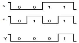
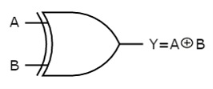
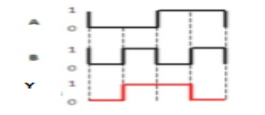
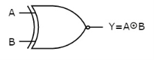
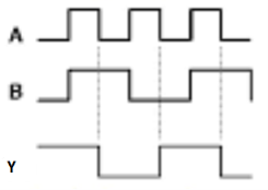
3.12 Ex-OR gate
It stands for Exclusive-OR gate. Its function varies when the inputs have even number of ones. The truth table of 2-input Ex-OR gate is:
Here A, B are the inputs and Y is the output of two input Ex-OR gate. The output (Y) is zero instead of one when both the inputs are one. Therefore, the output of Ex-OR gate is ‘1’, when only one of the two inputs is ‘1’. And it is zero, when both inputs are same. The symbol of Ex-OR gate is as follows: Fig.: XOR gate (ref. 1)
It is similar to that of OR gate with an exception for few combination(s) of inputs. Hence, the output is also known as an odd function.
Timing Diagram:
|
3.13 Ex-NOR gate
It stands for Exclusive-NOR gate. Its function is same as that of NOR gate except when the inputs having even number of ones. The truth table of 2-input Ex-NOR gate is:
Here A, B are the inputs and Y is the output. It is same as Ex-NOR gate with the only modification in the fourth row. The output is 1 instead of 0, when both the inputs are one. Hence the output of Ex-NOR gate is ‘1’, when both inputs are same and 0, when both the inputs are different. The symbol of Ex-NOR gate is: Fig.: XNOR gate (ref. 1) It is similar to NOR gate except for few combination(s) of inputs. Here the output is ‘1’, when even number of 1 is present at the inputs. Hence is also called as an even function.
Timing Diagram:
|
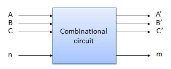
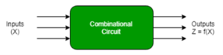
COMBINATIONAL CIRCUIT
A Combinational circuit is a circuit in which we combine the different gates. For example encoder, decoder, multiplexer, demultiplexer etc. Some of the characteristics are as follows −
Block diagram Fig. : Combinational circuit (ref.2 )
|
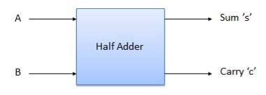
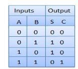
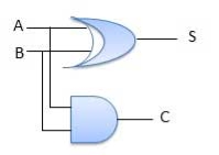
3.14 Half Adder
- It is a combinational circuit which has two inputs and two outputs.
- It is designed to add two single bit binary number A and B.
- It has two outputs carry and sum.
Fig. : Half adder (ref. 2)
Truth Table
Circuit Diagram Fig.: Half adder (ref. 2)
|
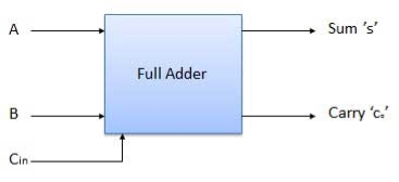
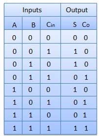
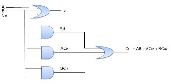
3.15 Full Adder
- It is developed to overcome the drawback of Half Adder circuit.
- It can add two one-bit numbers A and B and a carry C.
- It is a three input and two output combinational circuit.
Block diagram
Fig. : Full adder (ref. 2)
Circuit Diagram
Fig. : Full adder (ref. 2)
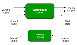
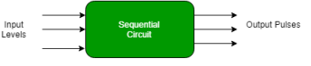
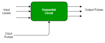
Sequential circuits
Fig. Combinational circuit
Fig. Sequential circuit There are two types of input to the combinational logic in fig 2 :
Secondary inputs are state variables that are produced by the storage elements where as secondary outputs are excitations for those storage elements. Types of Sequential Circuits – There are two types of sequential circuit :
Fig. Asynchronous Sequential circuit But they are more difficult to design and their output is also uncertain.
Fig. Synchronous Sequential circuit
|
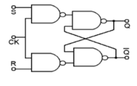
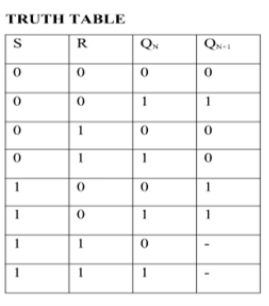
SR Flip Flop
JK Flip Flop
|
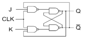
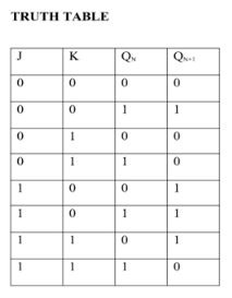
Race Around Condition In JK Flip-flop –
- For J-K flip-flop, if J=K=1, and if clk=1 for a long period of time, then output Q will toggle as long as CLK remains high which makes the output unstable or uncertain.
- This problem is known as race around condition in J-K flip-flop.
- This problem can be avoided by ensuring that the clock input is at logic “1” only for a very short time.
- Hence the concept of Master Slave JK flip flop was introduced.
Master Slave JK flip flop –
It is basically a combination of two JK flip-flops connected together in series.
- The first is the “master” and the other is a “slave”.
- The output from the master is connected to the two inputs of the slave whose output is fed back to inputs of the master.
- In addition to these two flip-flops, the circuit comprises of an inverter.
- The inverter is connected to clock pulse in such a way that an inverted clock pulse is given to the slave flip-flop.
- In other words if CP=0 for a master flip-flop, then CP=1 for a slave flip-flop and vice versa.
|
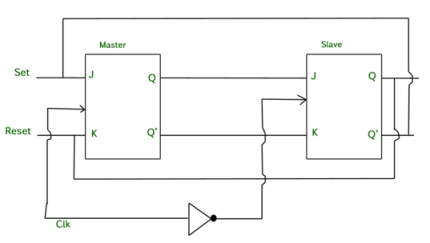
Fig. Master Slave Flip flop
Working of a master slave flip flop –
- When the clock pulse goes high, the slave is isolated; J and K inputs can affect the state of the system. The slave flip-flop is isolated when the CP goes low. When the CP goes back to 0, information is transmitted from the master flip-flop to the slave flip-flop and output is obtained.
- The master flip flop is positive level triggered and the slave flip flop is negative level triggered, hence the master responds prior to the slave.
- If J=0 and K=1, Q’ = 1 then the master goes to the K input of the slave and the clock forces the slave to reset therefore the slave copies the master.
- If J=1 and K=0, Q = 1 then the master goes to the J input of the slave and the Negative transition of the clock sets the slave and thus copy the master.
- If J=1 and K=1, the master toggles on the positive transition and the slave toggles on the negative transition of the clock.
- If J=0 and K=0, the flip flop becomes disabled and Q remains unchanged.
Timing Diagram of a Master flip flop –
|
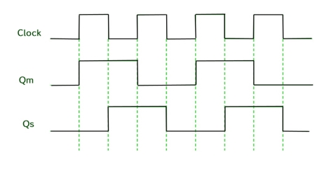
- When the CP = 1 then the output of master is high and remains high till CP = 0 because the state is stored.
- Now the output of master becomes low when the clock CP = 1 and remains low until the clock becomes high again.
- Thus toggling takes place for a clock cycle.
- When the CP = 1 then the master is operational but not the slave.
- When the clock is low, the slave becomes operational and remains high until the clock again becomes low.
- Toggling takes place during the whole process since the output changes once in a cycle.
- This makes the Master-Slave J-K flip flop a Synchronous device which passes data with the clock signal.
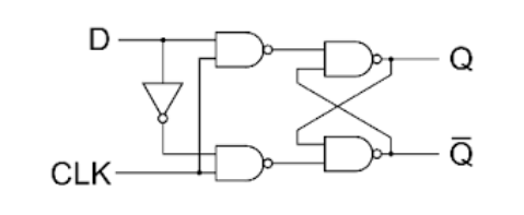
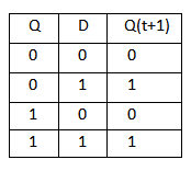
D Flip Flop
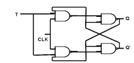
T Flip Flop
|

Microprocessor: Introduction
- It is a controlling unit that is fabricated on a small chip.
- It is capable to perform arithmetic logic operations and communicate with various devices connected to it.
- It comprises of an ALU (Arithmetic Logic Unit), MU (Memory unit) and CU (Control unit).
- It also consists of register array with registers named as B, C, D, E, H, L and ACC.
|
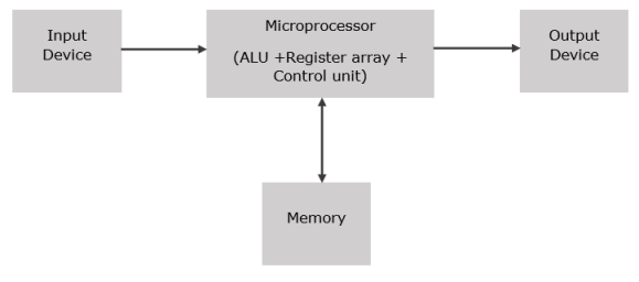
Fig.: Basic block diagram of microprocessor
Microcontroller: Introduction
- Microcontroller is a compact tiny computer that is fabricated inside a chip and is used in automatic control systems including security systems, office machines, power tools, alarming system, traffic light control, washing machine, and much more.
- It is economical programmable logic control that can be interfaced with external devices in order to control the devices from a distance.
- It was specially built for embedded system and consisted of read write memory, read only memory, I/O ports, processor and built in clock.
- C and assembly languages are used to program the microcontrollers.
- There are also other languages available to program the microcontroller but at the start learning a microcontroller programming with C and assembly language is a great choice, both are easy to learn and provide a clear concept about microcontroller.
- Technology have been evolved in an amazing way and made our lives easier more than ever before.
|
References
1. “Electronics Devices” by Thomas. L. Floyd, 9th Edition, Pearson (Unit I, II)
2. “Modern Digital Electronics” by R.P. Jain, 4th Edition, Tata McGraw Hill (Unit III)
3. “Electronic Instrumentation” by H.S. Kalsi, 3rd Edition, Tata McGraw Hill (Unit IV)
4. “Sensors and Transducers” by D. Patrnabis, 2nd Edition, PHI (Unit V)


