Unit-2
Combinational Logic Design

Example
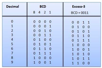
Fig.1: BCD to XS 3 conversion (Ref. 1)
2. Gray Code
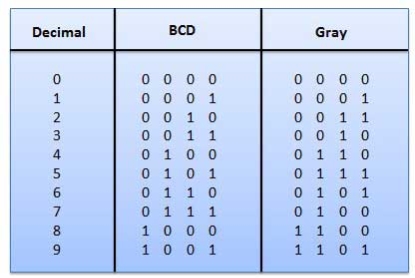
Fig.2: Gray codes (Ref. 1)
Application of Gray code
3. Binary Coded Decimal (BCD) code

Fig.3: BCD codes (Ref. 1)
Advantages of BCD Codes
Disadvantages of BCD Codes
4. Binary Code
Advantages of Binary Code
Classification of binary codes
The codes are broadly classified as:
Weighted Codes
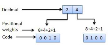
Fig.4: Weighted codes (Ref. 1)
Non-Weighted Codes
5. Alphanumeric codes
A binary digit orbit can be represented by two symbols as '0' or '1'.
This is not sufficient for communication between two computers as we need many more symbols for communication.
These symbols represent 26 alphabetic characters with capital and small letters, numbers from 0 to 9, punctuation marks, and other symbols.
These alphanumeric codes represent numbers and alphabetic characters.
Most of them also represent other characters like symbols and various instructions necessary for conveying information.
The code at least represents 10 digits and 26 letters of alphabet i.e. total of 36 items.
The following three types of alphanumeric codes are commonly used for data representation.
ASCII code is a 7-bit code whereas EBCDIC is an 8-bit code.
ASCII code is used worldwide while EBCDIC is primarily used in large IBM computers.
6. Error Codes
Their technique is available to detect and correct data during data transmission.
Error Code | Description |
Error detection and correction code techniques |
It is a combinational circuit that has two inputs and two outputs.
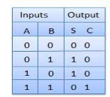
It is designed to add two single bit binary numbers A and B.
It has two outputs carry and sum.
Block diagram
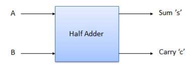
Fig. : A half adder (ref. 2)
Truth Table
Circuit Diagram
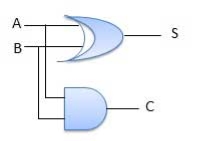
Fig.: A half adder (ref. 2)
B. Full Adder
It is developed to overcome the drawback of the Half Adder circuit.
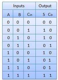
It can add two one-bit numbers A and B and a carry C.
It is a three-input and two output combinational circuit.
Block diagram
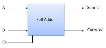
Fig. : Full adder (ref. 2)
Truth Table
Circuit Diagram
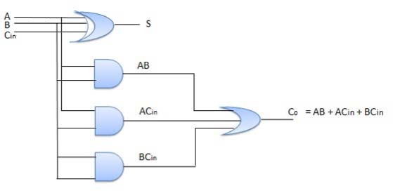
Fig.: Full adder (ref. 2)
C. Half Subtractors
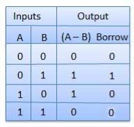
It is a combination circuit with two inputs and two outputs.
The difference between the two binary bits is obtained at the output and an output (Borrow) indicates if a 1 has been borrowed.
Here A is called Minuend bit and B is called a Subtrahend bit.
Truth Table
Circuit Diagram
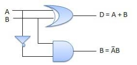
Fig.: Half subtractor (ref. 2)
D. Full Subtractors
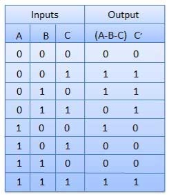
It is a combinational circuit which has three inputs A, B, C, and two output D and C'.
A is the 'minuend', B is 'subtrahend', C is the 'borrow' which is produced by the previous stage, difference output D and C' is the borrow output.
Truth Table
Circuit Diagram
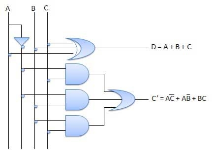
Fig.: Full subtractor (ref. 2)
E. Binary Adder (IC 7483)
F. BCD Adder
BCD stands for binary coded decimal.
Suppose, we have two 4-bit numbers A and B. The value of A and B can vary from 0(0000 in binary) to 9(1001 in binary).
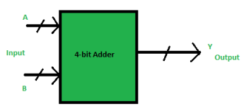
Fig. : BCD adder (ref. 2)
The output varies from 0 to 18 if the carry from the previous sum is not considered.
But if we consider the carry, then the maximum value of output will be 19 (i.e. 9+9+1 = 19).
When we simply add A and B, then we get the binary sum, and to get the output in BCD form, we use BCD Adder.
Example 1:
Input :
A = 0111 B = 1000
Output :
Y = 1 0101
Explanation: We are adding A(=7) and B(=8).
The value of the binary sum will be 1111(=15).
But, the BCD sum will be 1 0101,
where 1 is 0001 in binary and 5 is 0101 in binary.
Example 2:
Input :
A = 0101 B = 1001
Output :
Y = 1 0100
Explanation: We are adding A(=5) and B(=9).
The value of the binary sum will be 1110(=14).
But, the BCD sum will be 1 0100,
where 1 is 0001 in binary and 4 is 0100 in binary.
Now, let's move to the table and find out the logic when we are going to add “0110”.
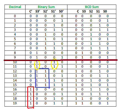
Fig. : Table explaining BCD addition (ref. 2)
We are adding “0110” (=6) only to the second half of the table because of the following conditions:
So, our logic is
C' + S3'.S2' + S3'.S1' = 1
Implementation :
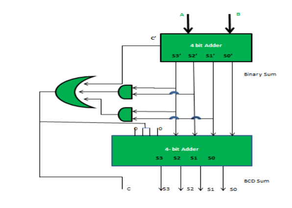
Fig. : BCD adder (ref. 2)
A carry-Lookahead adder is a fast parallel adder as it reduces the propagation delay by more complex hardware, hence it is costlier. In this design, the carry logic over fixed groups of bits of the adder is reduced to two-level logic, which is nothing but a transformation of the ripple carry design.
This method makes use of logic gates so as to look at the lower order bits of the augend and addend to see whether a higher order carry is to be generated or not.
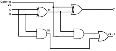
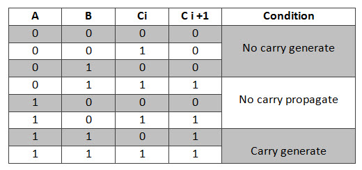
Consider the full adder circuit shown above with corresponding truth table. If we define two variables as carry generate Gi and carry propagate Pi then,
Pi = Ai ⊕ Bi
Gi = Ai Bi
The sum output and carry output can be expressed as
Si = Pi ⊕ Ci
C i +1 = Gi + Pi Ci
Where Gi is a carry generate which produces the carry when both Ai, Bi are one regardless of the input carry. Pi is a carry propagate and it is associate with the propagation of carry from Ci to Ci +1.
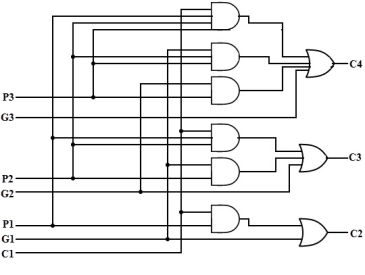
The carry output Boolean function of each stage in a 4 stage carry-Lookahead adder can be expressed as
C1 = G0 + P0 Cin
C2 = G1 + P1 C1
= G1 + P1 G0 + P1 P0 Cin
C3 = G2 + P2 C2
= G2 + P2 G1+ P2 P1 G0 + P2 P1 P0 Cin
C4 = G3 + P3 C3
= G3 + P3 G2+ P3 P2 G1 + P3 P2 P1 G0 + P3 P2 P1 P0 Cin
From the above Boolean equations we can observe that C4 does not have to wait for C3 and C2 to propagate but actually C4 is propagated at the same time as C3 and C2. Since the Boolean expression for each carry output is the sum of products so these can be implemented with one level of AND gates followed by an OR gate.
The implementation of three Boolean functions for each carry output (C2, C3 and C4) for a carry-Lookahead carry generator shown in below figure.
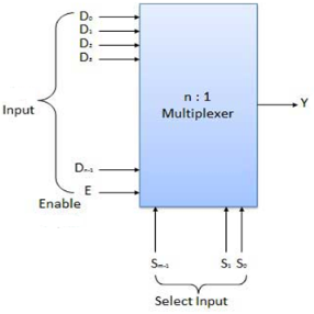
Fig. : Block diagram of the multiplexer (ref. 2)
Multiplexers come in multiple variations
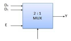
Block Diagram of 2:1 MUX
Truth Table of 2:1 MUX
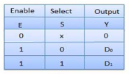
Where x is don’t care.
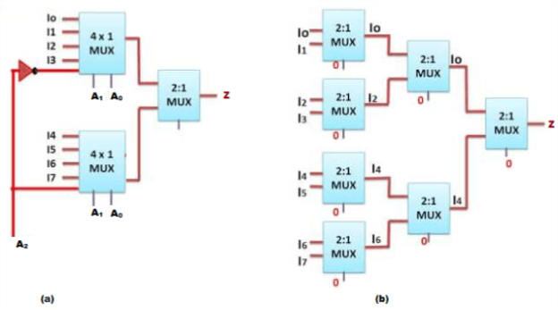
Cascading refers to a process where large Multiplexers can be designed and implemented using smaller Multiplexers. Example: 8:1 Mux can be designed using two 4:1 Multiplexers and similarly it can be designed using four 2:1 Multiplexers as shown in the below figure.
Demultiplexers
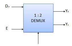
Various Demultiplexers are used as:
Block diagram
Truth Table
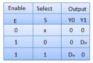
Where x is don’t care.
MUX
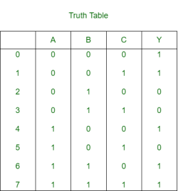
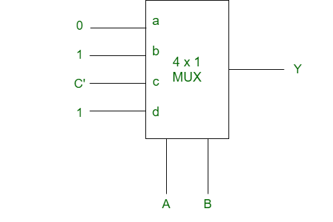
Given SOP function f(A, B, C) = m(0, 1, 4, 6, 7) and MUX is
For 3 variable function, the truth table is
Let A and B are the select lines and C be the input,
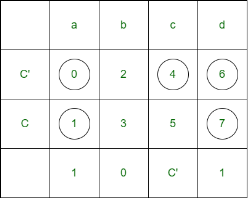
Thus, for the implementation of given logical function, required is one 4×1 MUX and and inverter.
2-Bit Magnitude Comparator
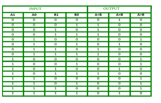
K-map for each output is as follows:
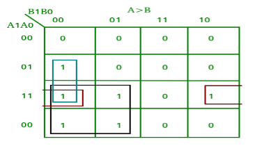
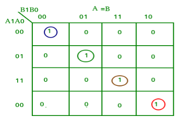
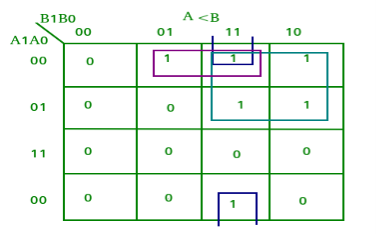
From the above K-maps output can be expressed as follows:
A>B:A1B1’ + A0B1’B0’ + A1A0B0’
A=B: A1’A0’B1’B0’ + A1’A0B1’B0 + A1A0B1B0 + A1A0’B1B0’
: A1’B1’ (A0’B0’ + A0B0) + A1B1 (A0B0 + A0’B0’)
: (A0B0 + A0’B0’) (A1B1 + A1’B1’)
: (A0 Ex-Nor B0) (A1 Ex-Nor B1)
A<B:A1’B1 + A0’B1B0 + A1’A0’B0
A logic circuit for this comparator as given below:
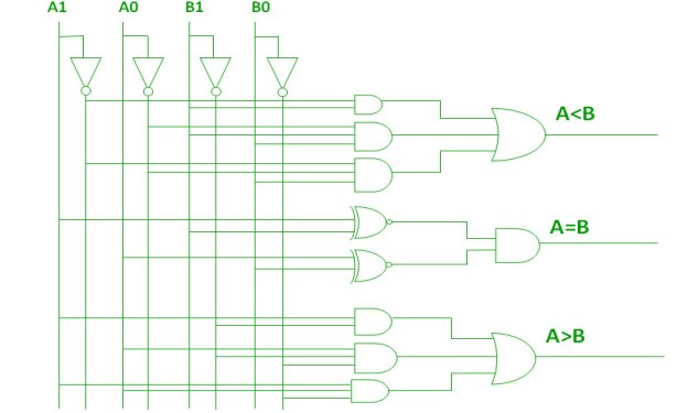
Fig:-bit comparator (ref.2)
Even Parity Generator
A 3-bit message is transmitted with an even parity bit. Hence assuming, the three inputs W,X and Y that are applied to the circuits and output bit is the parity bit P. The total number of 1s must be even, to generate the even parity bit P.
3- bit message | Even Parity | ||
W | X | Y | P |
0 | 0 | 0 | 0 |
0 | 0 | 1 | 1 |
0 | 1 | 0 | 1 |
0 | 1 | 1 | 0 |
1 | 0 | 0 | 1 |
1 | 0 | 1 | 0 |
1 | 1 | 0 | 0 |
1 | 1 | 1 | 1 |
The K-map simplification for 3-bit message even parity generator is
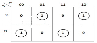
From the above K-Map, the expression is:
P=W′X′Y+W′XY′+WX′Y′+WXY
P=W′(X′Y+XY′)+W(X′Y′+XY)
P=W′(X⊕Y)+W(X⊕Y)′=W⊕X⊕Y

Odd Parity Generator
Considering that the 3-bit data is transmitted with an odd parity bit. The three inputs are W, X and Y and P is the output parity bit. The total number of bits must be odd in order to generate the odd parity bit.
3- bit message | Odd Parity | ||
W | X | Y | P |
0 | 0 | 0 | 1 |
0 | 0 | 1 | 0 |
0 | 1 | 0 | 0 |
0 | 1 | 1 | 1 |
1 | 0 | 0 | 0 |
1 | 0 | 1 | 1 |
1 | 1 | 0 | 1 |
1 | 1 | 1 | 0 |
The K-map simplification for 3-bit message even parity generator is
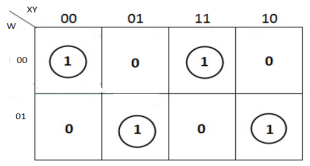

Parity Checker
Even parity checker
Assume a 3-bit binary input, W, X and Y is transmitted along with an even parity bit, P. So, the resultant data contains 4 bits, that is received as the input of even parity checker.
It generates an even parity bit, E. This bit is zero, if the received data contains an even number of ones, which indicates that there is no error in the received data and vice versa.
The Truth table of an even parity checker is:
4-bit Received Data WXYP | Even Parity Check bit E |
0000 | 0 |
0001 | 1 |
0010 | 1 |
0011 | 0 |
0100 | 1 |
0101 | 0 |
0110 | 0 |
0111 | 1 |
1000 | 1 |
1001 | 0 |
1010 | 0 |
1011 | 1 |
1100 | 0 |
1101 | 1 |
1110 | 1 |
1111 | 0 |
The Boolean function of even parity check bit as
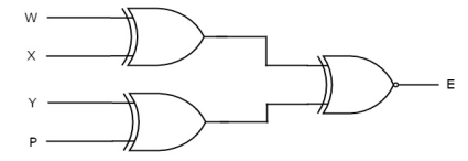
E = W xor X xor Y xor P
The following figure shows the circuit diagram of even parity checker.
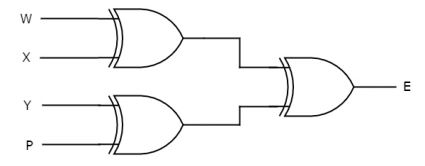
Odd Parity Checker
Assume a 3-bit binary input, W, X and Y is transmitted along with an odd parity bit, P. So, the resultant data contains 4 bits, that is received as the input of odd parity checker.
It generates an odd parity bit, E. This bit is zero, if the received data contains an odd number of ones, which indicates there is no error in the received data.
Reference Books:
1. John Yarbrough, ―Digital Logic Applications and Design, Cengage Learning, ISBN – 13: 978-81-315-0058-3
2. D. Leach, Malvino, Saha, ―Digital Principles and Applications‖, Tata McGraw Hill, ISBN – 13:978-0-07-014170-4.
3. Anil Maini, ―Digital Electronics: Principles and Integrated Circuits‖, Wiley India Ltd, ISBN:978-81-265-1466-3.
4. Norman B & Bradley, ―Digital Logic Design Principles, Wiley India Ltd, ISBN:978-81-265-1258
