Unit-3
Sequential Logic Design
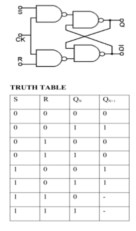
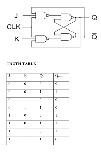
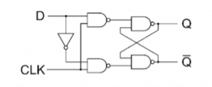
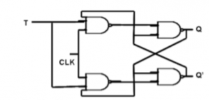
Logic diagrams and truth tables of the various types of flip-flops are as follows:
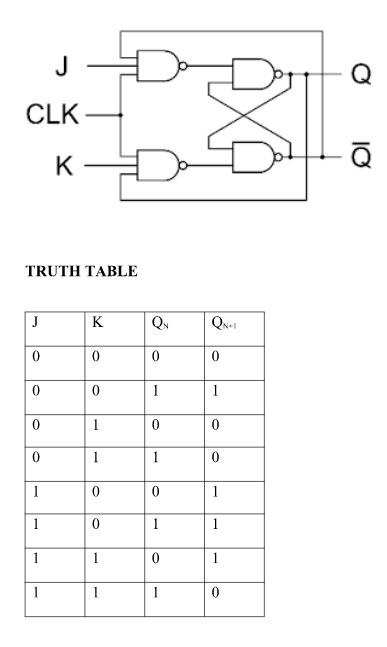
2. J-K Flip Flop:
3. D Flip Flop :
4. T Flip Flop :
As flip flop may come up in random states when power is switched on, it is necessary to use some method where all the flip flops can be set or reset at the same time by a single switch – it is inconvenient to set or reset each flip flop
individually. This is achieved by incorporating PRESET and CLEAR inputs in flip flops which can over-write all other inputs. These I/Ps are asynchronous and independent of the clock. While they are present, all other operations are inhibited. They force the output to a certain state irrespective of the I/Ps and clock.
Active High
Active High means that Preset and Clear I/Ps are inactive when low.
Pr = 1, Q = 1, Q’ = 0
i.e. if the Preset I/P is 1, the output will be forced to SET state irrespective of other I/Ps.
Cr = 1, Q = 0, Q’ = 1
i.e. if the Clear I/P is 1, the output will be forced to RESET state irrespective of other I/Ps.
It is not possible to Preset and Clear a flip flop at the same instant of time as Q can’t be 0 and 1 at the same time.
i.e. Pr = Cr ≠ 1 at any instant.
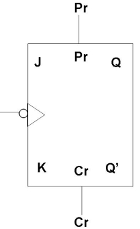
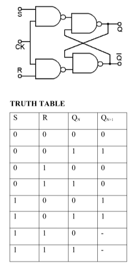
Fig. Master-Slave Flip flop
Working of a master-slave flip flop –
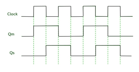
Timing Diagram of a Master flip flop –
Conversion for FlipFlops:-
EXCITATION TABLE:
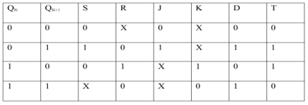
i) SR To JK FlipFlop
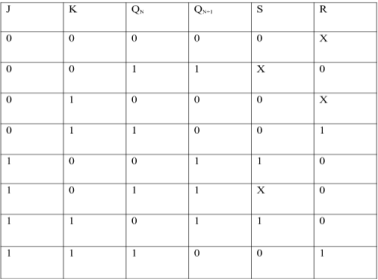
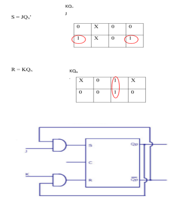
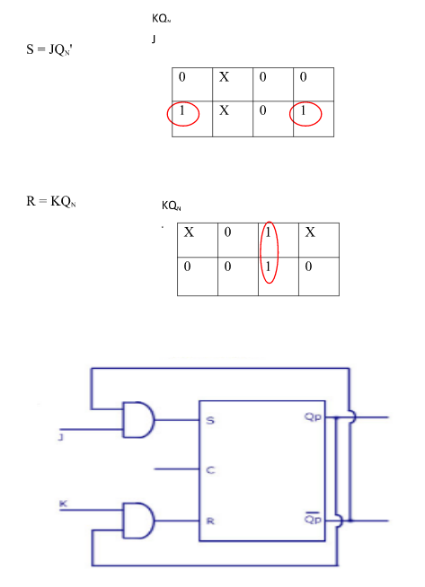
Excitation Functions:
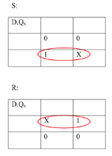
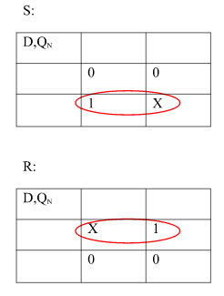
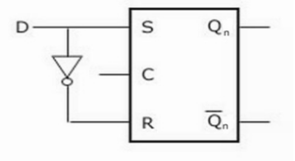
ii) Convert SR To D FlipFlop:
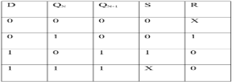
Excitation Functions:
S = D
R = D‘
The registers which shift the bits towards the right are called “Shift right registers”.
Shift registers are of 4 types and they are:
Serial-In Serial-Out Shift Register (SISO) –
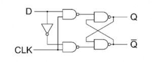
Fig. SISO
Serial-In Parallel-Out shift Register (SIPO) –
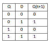
Fig. SIPO
Parallel-In Serial-Out Shift Register (PISO) –
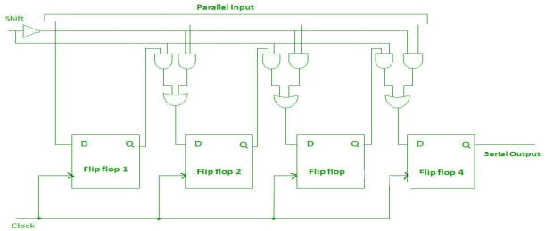
Fig. PISO
Parallel-In Parallel-Out Shift Register (PIPO) –
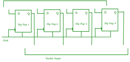
Fig. PIPO
Bidirectional Shift Register –
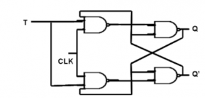
Fig. Bidirectional shift register
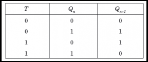

Fig. Ring counter
Universal Shift Register:
It comprises n flip-flops and n 4×1 multiplexers.
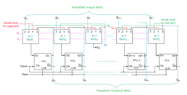
Fig. The N-bit universal shift register
S1 | S0 | REGISTER OPERATION |
0 | 0 | No changes |
0 | 1 | Shift right |
1 | 0 | Shift left |
1 | 1 | Parallel load |
Asynchronous Counter

Fig. Asynchronous counter
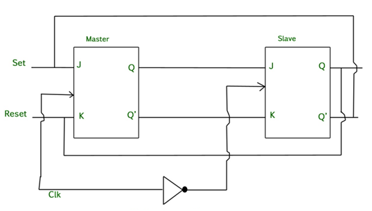
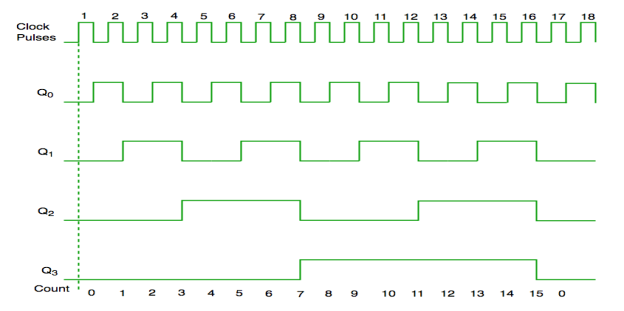
Fig. The timing diagram of Asynchronous counter
Synchronous Counter
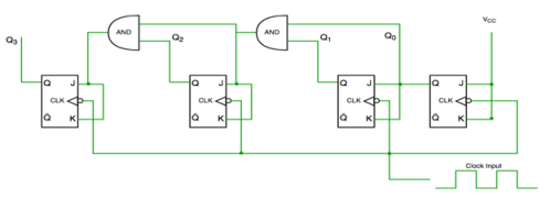
Fig. synchronous counter
Fig. Timing diagram of the synchronous counter
BCD Counter
This BCD counter uses d-type flip-flops, and this particular design is a 4-bit BCD counter with an AND gate. BCD counters usually count up to ten, also otherwise known as MOD 10. Since a 4-bit counter counts from binary 0 0 0 0 to binary 1 1 1 1, which is up to 16, we need a way to stop the count after ten, and we achieve this using an AND gate to initiate a reset. The 4-bit binary pattern for decimal ten is 1 0 1 0, and this is the only time when we see this pattern, therefore we can use the 1’s and feed them into an AND gate, which should produce a HIGH output, which can then reset all the flip-flops simultaneously, thereby stopping the count.
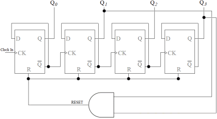
Understanding MSB and LSB
Decimal | 8 | 4 | 2 | 1 |
Outputs | Q3 | Q2 | Q1 | Q0 |
Position | MSB |
|
| LSB |
Binary | 1 | 0 | 1 | 0 |
The first thing to identify is the most significant bit (MSB), and least significant bit (LSB) concerning the outputs Q0, Q1, Q2, Q3. If you do not get this part right, then you will trip-up when it comes to connecting the AND gate.
The way I remember it is that this counter always starts with the smallest number, which appears first at Q0, therefore it has to be the LSB end.
As you can see from the table above, the outputs Q3 and Q1 contain the 1’s and therefore we connect these outputs to the AND gate.
Johnson Counter –
It is a shift register counter whose output of the first flip flop is connected to the second and so on and then an inverted output of the last flip flop is sent back to the first flip flop.
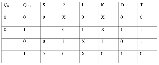
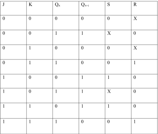
Fig. Johnson counter
Modulus of the counter ( IC 7490)
Truth table is as follows:
Clock pulse | Q3 | Q2 | Q1 | Q0 |
0 | 0 | 0 | 0 | 0 |
1 | 0 | 0 | 0 | 1 |
2 | 0 | 0 | 1 | 0 |
3 | 0 | 0 | 1 | 1 |
4 | 0 | 1 | 0 | 0 |
5 | 0 | 1 | 0 | 1 |
6 | 0 | 1 | 1 | 0 |
7 | 0 | 1 | 1 | 1 |
8 | 1 | 0 | 0 | 0 |
9 | 1 | 0 | 0 | 1 |
10 | 0 | 0 | 0 | 0 |
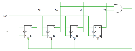
Fig. Decade counter
In the above circuit diagram we used nand gate for Q3 and Q1 and sending this to clear input line as the binary representation of 10 is—
1010
And Q3 and Q1 are 1 here, if we give NAND of these two bits then counter clears at 10 and again starts from the beginning.
Mealy Machine
A Mealy Machine is an FSM whose output depends on the present state as well as the present input.
It can be described by a 6 tuple (Q, ∑, O, δ, X, q0) where −
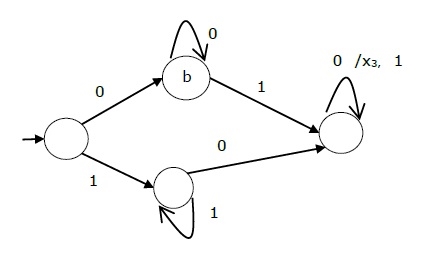
The state table of a Mealy Machine is shown below −
Present state | Next state | |||
input = 0 | input = 1 | |||
State | Output | State | Output | |
→ a | b | x1 | c | x1 |
b | b | x2 | d | x3 |
c | d | x3 | c | x1 |
d | d | x3 | d | x2 |
The state diagram of the above Mealy Machine is −
Moore Machine
Moore machine is an FSM whose outputs depend on only the present state.
A Moore machine can be described by a 6 tuple (Q, ∑, O, δ, X, q0) where −
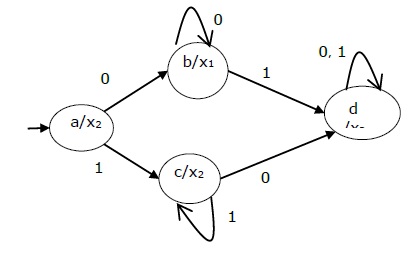
The state table of a Moore Machine is shown below −
Present state | Next State | Output | |
Input = 0 | Input = 1 | ||
→ a | b | c | x2 |
b | b | d | x1 |
c | c | d | x2 |
d | d | d | x3 |
The state diagram of the above Moore Machine is −
Mealy Machine vs. Moore Machine
The following table highlights the points that differentiate a Mealy Machine from a Moore Machine.
Mealy Machine | Moore Machine |
Output depends both upon the present state and the present input | Output depends only upon the present state. |
Generally, it has fewer states than Moore Machine. | Generally, it has more states than Mealy Machine. |
The value of the output function is a function of the transitions and the changes, when the input logic on the present state is done. | The value of the output function is a function of the current state and the changes at the clock edges, whenever state changes occur. |
Mealy machines react faster to inputs. They generally react in the same clock cycle. | In Moore machines, more logic is required to decode the outputs resulting in more circuit delays. They generally react one clock cycle later. |
Sequence Generator:
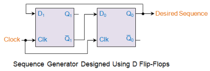
The sequence generators are nothing but a set of digital circuits which are designed to result in a specific bit sequence at their output. There are several ways in which these circuits can be designed including those which are based on multiplexers and flip-flops. Here in this article we deal with the designing of sequence generator using D flip-flops.
As an example, let us consider that we intend to design a circuit which moves through the states 0-1-3-2 before repeating the same pattern. The steps involved during this process are as follows.
For example, look at the orange shaded row in Table I in which the present and the next states 1 and 0 (respectively) result in D1 to be 0. The same row also shows the case wherein
Present States | Next States | Inputs of D flip-flops | |||
Q1 | Q0 | Q1+ | Q0+ | D1 | D0 |
0 | 0 | 0 | 1 | 0 | 1 |
0 | 1 | 1 | 1 | 1 | 1 |
1 | 1 | 1 | 0 | 1 | 0 |
1 | 0 | 0 | 0 | 0 | 0 |
Now its time to derive the Boolean expressions for D1 and D0. This can be done using any kind of simplification technique including K-map. However as our example is quite simple, we can just use the Boolean laws to solve for D1 and D0. Thus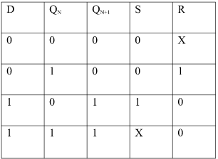
Having known the inputs to either of the D flip-flops, now we can design our sequence generator as shown in this figure.
Sequence detector
It is a sequential state machine that takes an input string of bits and generates an output 1 whenever the target sequence has been detected.
In a Mealy machine, output depends on the present state and the external input (x).
Hence the output is written outside the states, along with inputs.
Sequence detector is of two types:
In an overlapping sequence detector, the last bit of a sequence becomes the first bit of the next one.
In a non-overlapping sequence detector, the last bit of one sequence does not become the first bit of the next one.
Examples:
For non-overlapping case
Input :0110101011001
Output:0000100010000
For overlapping case
Input :0110101011001
Output:0000101010000
The steps to design a non-overlapping 101 Mealy sequence detector are:
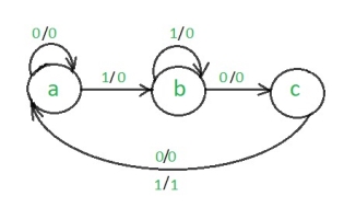
Step 1: Development of the state diagram –
The state diagram of a Mealy machine for a 101 sequence detector is:
Step 2: Assignment of the code–
Rule 1: States having the same next states for a given input condition should have adjacent assignments.
Rule 2:States that are the next states to a single state must be given adjacent assignments.
Rule 1 given preference over Rule 2.
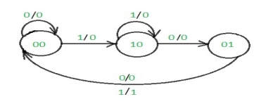
The state diagram after the code assignment is:
Step 3: Making Present State/Next State table –
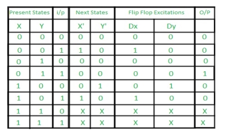
Step 4: Draw K-maps for Dx, Dy, and output (Z) –
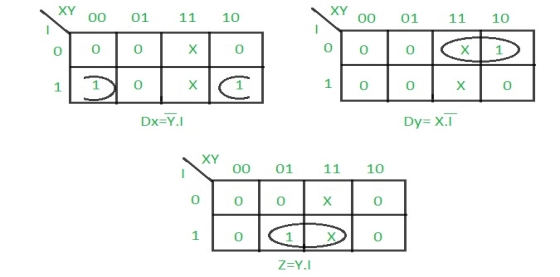
Step 5: Final implementation of the circuit –
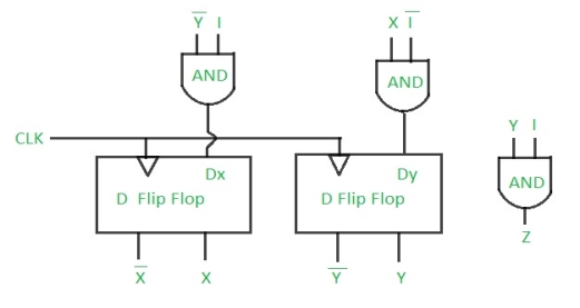
This is the desired circuit for a Mealy 101 non-overlapping sequence detector.
Reference Books:
1. John Yarbrough, ―Digital Logic Applications and Design, Cengage Learning, ISBN – 13: 978-81-315-0058-3
2. D. Leach, Malvino, Saha, ―Digital Principles and Applications‖, Tata McGraw Hill, ISBN – 13:978-0-07-014170-4.
3. Anil Maini, ―Digital Electronics: Principles and Integrated Circuits‖, Wiley India Ltd, ISBN:978-81-265-1466-3.
4. Norman B & Bradley, ―Digital Logic Design Principles, Wiley India Ltd, ISBN:978-81-265-1258
