Unit-5
Logic Families
Based on the fabrication technology, logic families are classified into two types: Bipolar logic family and Unipolar logic family.
Unipolar Logic Family: In unipolar logic families, unipolar devices are the key element. MOSFET (Metal Oxide Semiconductor Field Effect Transistor) is a unipolar device, in which the current flows because of only one type of charge carriers (that is, either electrons or holes). The examples of unipolar families include PMOS, NMOS, and CMOS
Bipolar Logic Family: Transistors and diodes are bipolar devices, in which the current flows because of both the charge carriers (electrons and holes). In bipolar logic families, transistors and diodes are used as key element.
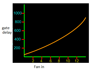
Fan-in:
| |
| |
Fig.: Effects of Fan-in | |
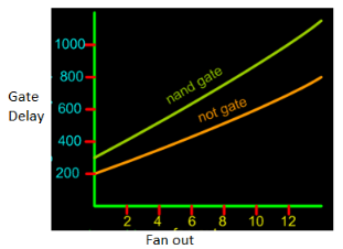
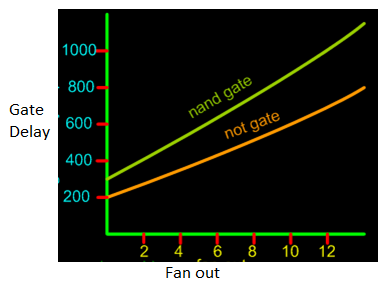
Fan-out:
| |
| |
| |
| |
| |
| |
Fig.: Effects of Fan-out | |
Gate circuits are made to sustain variations in input and output voltage levels. Variations are usually the result of various factors. |
|
|
|
|
|
|
The time between the logic transition on an input and the corresponding logic transition on the output of the logic gate. It is measured at midpoints.
|
|
Every gate is connected to a power supply VCC (VDD in the case of CMOS). A certain amount of current is drawn during its operation. Since each gate can be in a High, Transition or Low state, hence there are three types of currents drawn from power supply: |
|
|
|
For TTL, |
|
Average Power Dissipation = Vcc * (ICCH + ICCL)/2 |
|
For CMOS, |
|
Average Power Dissipation = Vcc * ICCT. |
|
For the TTL logic family, power dissipation does not depend on the frequency of operation. For CMOS, power dissipation depends on the frequency of operation. Power Dissipation: |
|
Power dissipation of a circuit defines its battery life: the greater the power dissipation, the shorter the battery life. It is directly proportional to the heat generated by the chip or system hence excessive heat dissipation may increase operating temperature and cause gate circuitry to drift out of its normal operating range. |
Total power dissipation = static power dissipation + dynamic power dissipation. |
Figure of merit is a product of propagation delay and power dissipation. It is measured in terms of Pico-Joules (ns ´mW = pJ). Current and voltage parameters define the minimum and maximum limit of current and voltage for input and output of a logic family.
They are built only with the help of transistors. It has been improved to meet performance requirements. TTL family comprises of: |
|
|
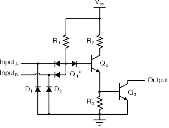
Operation of TTL NAND Gate (Two input )
The circuit diagram of a 2 input TTL NAND gate is as follows:
a) A and B both low: both B-E junctions of Q1 are forward biased. Hence D1 and D2 will conduct to force the voltage at point C to 0.7V. This voltage is insufficient to forward bias B-E junction of Q2. Hence Q2 remains OFF. Therefore its collector voltage rises to VCCVCC. As Q3 is operating in emitter follower mode, output Y will be pulled up to high voltage Y= 1
b) Either A or B low: If any one input is connected to ground with other left open or connected to VCCVCC the corresponding diode (D1 or D2) will conduct. This will pull down voltage at C o 0.7V. This voltage is insufficient to turn on Q2 so it remains OFF. So collector voltage of Q2 will be equal to VCC. This voltage acts as base voltage for Q3. As Q3 acts as an emitter follower, output Y will be pulled to VCCVCC. Y= 1
c) A and B both high: If both A and B are connected to then both diodes D1 and D2 will be reverse biased and do not conduct. Therefore D3 is forward biased and base current is supplied to transistor Q2 via R1 and D3. As Q2 conducts, the voltage at X will drop down and Q3 will be OFF, whereas voltage at Z will increase to turn ON Q4. As Q4 goes into saturation, the output voltage Y will be pulled down to low. Y = 0
TTL with active pull up
It is possible in TTL gates the charging of output capacitance without corresponding increase in power dissipation with the help of an output circuit arrangement referred to as an active pull-up or totem-pole output. In this case,
• Outputs must never be connected together.
• Connecting outputs causes excessively high currents to flow.
•Outputs will eventually be damaged.
• The standard TTL output configuration with a HIGH output and a LOW output transistor, only one of which is active at any time.
• A phase splitter transistor controls which transistor is active.
TTL with open collector output
The main feature is that its output is 0 when low and floating when high. Usually, an external Vcc may be applied.
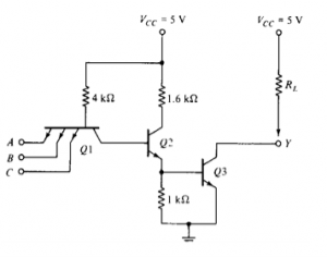
Transistor Q1 behaves as a cluster of diodes placed back to back. With any of the input at logic low, the corresponding emitter-base junction is forward biased and the voltage drop across the base of Q1 is around 0.9V, not enough for the transistors Q2 and Q3 to conduct. Thus the output is either floating or Vcc, i.e. High level.
Similarly, when all inputs are high, all base-emitter junctions of Q1 are reverse biased and transistor Q2 and Q3 get enough base current and are in saturation mode. The output is at logic low. (For a transistor to go to saturation, collector current should be greater than β times the base current).
Totem Pole Output:
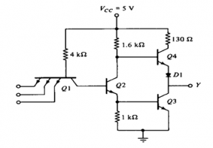
Totem Pole means the addition of an active pull up the circuit in the output of the Gate which results in a reduction of propagation delay.

Logic operation is the same as the open collector output. The use of transistors Q4 and diode is to provide quick charging and discharging of parasitic capacitance across Q3. The resistor is used to keep the output current to a safe value.
Three state Gate:
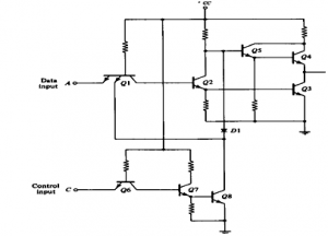
It provides 3 state output.
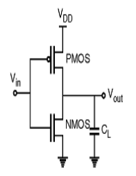
CMOS Inverter
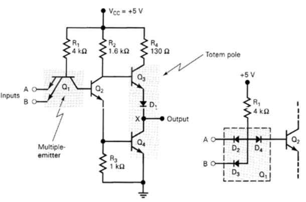
Fig: CMOS inverter
A | Y = A’ |
0 | 1 |
1 | 0 |
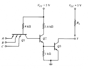
Fig. : NOT gate (ref. 1)
CMOS characteristics
The VTC is divided into five regions(1-5) for easy of understanding. The above shown curve is possible when both T1 and T2 are matched for optimum operation. Optimum operation is achieved when Vin = Vdd/2 we get Vout = Vdd/2 . This can be achieved by adjusting width and length of both T1 and T2 as other parameters like mobility, oxide capacitance vary between different technologies.

Region-1
In this, the input is in the range of (0,Vtn).
Region-2
Here, the input is in the range of (Vtn,Vdd/2).
Region-3
Here the input voltage is Vdd/2. At this point the output voltage is Vdd/2. Here both the NMOS and PMOS are in saturation and the output drops drastically from Vdd to Vdd/2. At this point a large amount of current flows from the supply.
Region-4
In this region the input voltage is in the range of (Vdd/2 ,Vdd-Vtp). Here the PMOS remains in saturation as Vout< Vin - Vtp and Vgsp<Vtp. But the NMOS moves from saturation to linear region since the drain to source voltage now is less than Vgsn-Vtn.
Region-5
In this region the input voltage is in the range of (Vdd-Vtp,Vdd). Here the PMOS moves from saturation to cutoff as the Vgsp is so high that Vgsp>Vtp. The NMOS still remains in linear as the drain to source voltage now is less than Vgsn-Vtn.
CMOS configurations- Wired Logic, Open-drain outputs
Open Drain is a type of programmable output port configuration with push pull,input only, and quasi-bidirectional configurations. Open-collector/open-drain is a circuit technique which allows multiple devices to communicate bidirectionally on a single wire. This is basically a mode which provides just a pull down operation.
An open collector/open drain is a common type of output found on many integrated circuits (IC). Instead of outputting a signal of a specific voltage or current, the output signal is applied to the base of an internal NPN transistor whose collector is externalized (open) on a pin of the IC. The emitter of the transistor is connected internally to the ground pin. If the output device is a MOSFET the output is called open drain and it functions in a similar way.
Reference Books:
1. John Yarbrough, ―Digital Logic Applications and Design, Cengage Learning, ISBN – 13: 978-81-315-0058-3
2. D. Leach, Malvino, Saha, ―Digital Principles and Applications‖, Tata McGraw Hill, ISBN –13:978-0-07-014170-4.
3. Anil Maini, ―Digital Electronics: Principles and Integrated Circuits‖, Wiley India Ltd, ISBN:978-81-265-1466-3.
4. Norman B & Bradley, ―Digital Logic Design Principles, Wiley India Ltd, ISBN:978-81-265-1258


