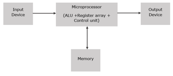
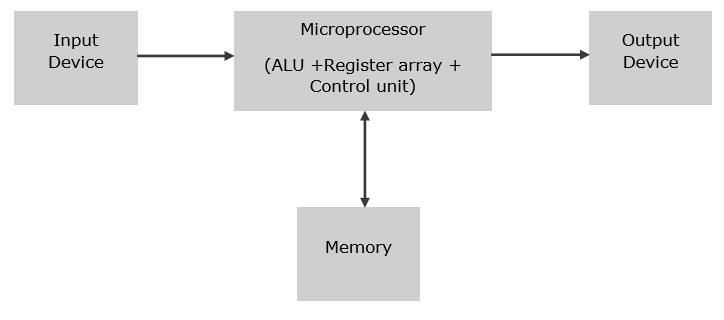
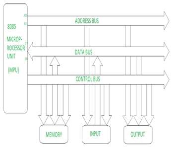
Fig.: Basic block diagram of microprocessor (ref 1)
Basic functions of microprocessor
It is an 8-bit register used for performing all arithmetical and logical operations. It is also used to load and store data.
It performs all arithmetical and logical operations like add, subtract, AND, OR etc.
There are 6 General purpose registers and they are B, C, D, E, H and L. Each of them can hold 8 bit of data. They can also work in pair known as register pairs and they are H-L, B-C and D-E.
It is a 16 bit register. It is used to store data, memory information etc. whenever memory is incremented, the PC then points to the next location.
It is a 16 bit register. It always points to stack which can be incremented or decremented by PUSH and POP instruction.
It is an 8 bit register which is used to store temporary information of the ALU.
It is an 8 bit register.

Here, Sign (S), Zero (Z), Auxiliary Carry (AC), Parity (P),Carry (C) bit.
It is an 8-bit register. It stores an instruction that is fetched from memory. It decodes the information present inside it.
It provides timing and control signal to the microprocessor to perform various operations. Following are the signals that controls the external and internal circuits are:
Control Signals: READY, RD’, WR’, ALE
Status Signals: S0, S1, IO/M’
DMA Signals: HOLD, HLDA
RESET Signals: RESET IN, RESET OUT D7
It controls the interrupts during a process. When a microprocessor is executing a main program and if an interrupt occurs, the microprocessor shifts the control from the main program to process the incoming request. After the request is completed, the control goes back to the main program.
There are 5 types of interrupts: INTR, RST 7.5, RST 6.5, RST 5.5 and TRAP.
It controls the serial data communication in the microprocessor by using two instructions namely SID (Serial input data) and SOD (Serial output data).
Data bus carries the data required to be stored. It is bidirectional. Address bus carries the location to where the data should be stored and it is unidirectional. It is used to transfer the data & address.
System Bus
Address bus
It is a 16-bit bus in which A15-A8, it carries the most significant 8-bits of memory/IO address and AD7-AD0 are multiplexed with data lines that carries the least significant bits of the address.
As its length is 16 Bit, it ranges from 0000 H to FFFF H, where H denotes Hexadecimal. The microprocessor 8085 can transfer a maximum of 16 bit address which means it can address 65, 536 different memory location.
Data bus
It is an 8-bit bus which is multiplexed with the address lines AD7-AD0. It carries data and also the least significant 8-bit address.
Its length is 8 Bit which ranges from 00 H to FF H where H denotes Hexadecimal.
Control Bus
It is used to send control signals to all the associated peripherals. It is used to process data. Some of the control signals are:
Memory read
Memory write
I/O read
I/O Write
Opcode fetch

Fig.: System Bus (ref 1)
Basic operations of microprocessor
It is an 8-bit register used for performing all arithmetical and logical operations. It is also used to load and store data.
It performs all arithmetical and logical operations like add, subtract, AND, OR etc.
There are 6 General purpose registers and they are B, C, D, E, H and L. Each of them can hold 8 bit of data. They can also work in pair known as register pairs and they are H-L, B-C and D-E.
It is a 16 bit register. It is used to store data, memory information etc. whenever memory is incremented, the PC then points to the next location.
It is a 16 bit register. It always points to stack which can be incremented or decremented by PUSH and POP instruction.
It is an 8 bit register which is used to store temporary information of the ALU.
It is an 8 bit register.
Here, Sign (S), Zero (Z), Auxiliary Carry (AC), Parity (P),Carry (C) bit.
It is an 8-bit register. It stores an instruction that is fetched from memory. It decodes the information present inside it.
It provides timing and control signal to the microprocessor to perform various operations. Following are the signals that controls the external and internal circuits are:
Control Signals: READY, RD’, WR’, ALE
Status Signals: S0, S1, IO/M’
DMA Signals: HOLD, HLDA
RESET Signals: RESET IN, RESET OUT D7
It controls the interrupts during a process. When a microprocessor is executing a main program and if an interrupt occurs, the microprocessor shifts the control from the main program to process the incoming request. After the request is completed, the control goes back to the main program.
There are 5 types of interrupts: INTR, RST 7.5, RST 6.5, RST 5.5 and TRAP.
It controls the serial data communication in the microprocessor by using two instructions namely SID (Serial input data) and SOD (Serial output data).
Data bus carries the data required to be stored. It is bidirectional. Address bus carries the location to where the data should be stored and it is unidirectional. It is used to transfer the data & address.
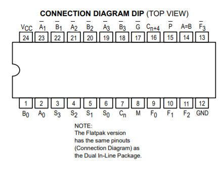
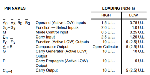
ALU using IC 74181
The SN54/74LS181 is a 4-bit Arithmetic Logic Unit (ALU) which can perform all the possible 16 logic, operations on two variables and a variety of arithmetic operations.
• Provides 16 Arithmetic Operations Add, Subtract, Compare, Double, Plus Twelve Other Arithmetic Operations
• Provides all 16 Logic Operations of Two Variables Exclusive — OR, Compare, AND, NAND, OR, NOR, Plus Ten other Logic Operations
• Full Lookahead for High Speed Arithmetic Operation on Long Words
• Input Clamp Diodes
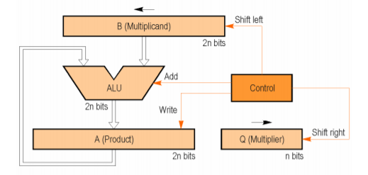
4-bit Multiplier circuit using ALU and shift registers
Shift-and-add multiplication is similar to the multiplication performed by paper and pencil. This method adds the multiplicand X to itself Y times, where Y denotes the multiplier. To multiply two numbers by paper and pencil, the algorithm is to take the digits of the multiplier one at a time from right to left, multiplying the multiplicand by a single digit of the multiplier and placing the intermediate product in the appropriate positions to the left of the earlier results. As an example, consider the multiplication of two unsigned 4-bit numbers, 8 (1000) and 9 (1001).
In the case of binary multiplication, since the digits are 0 and 1, each step of the multiplication is simple. If the multiplier digit is 1, a copy of the multiplicand (1 × multiplicand) is placed in the proper positions; if the multiplier digit is 0, a number of 0 digits (0 × multiplicand) are placed in the proper positions.
|
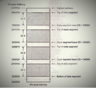
Fig.: Memory Segmentation
|
|
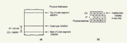
Fig.: 20-bit address generation |

Reference Books:
1. John Yarbrough, ―Digital Logic Applications and Design, Cengage Learning, ISBN – 13: 978-81-315-0058-3
2. D. Leach, Malvino, Saha, ―Digital Principles and Applications‖, Tata McGraw Hill, ISBN – 13:978-0-07-014170-4.
3. Anil Maini, ―Digital Electronics: Principles and Integrated Circuits‖, Wiley India Ltd, ISBN:978-81-265-1466-3.
4. Norman B & Bradley, ―Digital Logic Design Principles, Wiley India Ltd, ISBN:978-81-265-1258
