UNIT 6
Nanotechnology
In the field of the nanotechnology innovation and research concerned with the developing” things”, normally, devices and materials, on scale of molecules and atoms. A nanometer is 1 billionth of a meter, 10 times hydrogen diameter atom. Human hair diameter is on average, 80000, nanometers. At that scales, the simple rules of chemistry and physics no longer applicable. For example, characteristics of materials, like their color, reactivity, conductivity and strength can vary substantially between macro and nanoscale. Carbon ‘nanotubes’ are hundred times stronger than the steel but 6 times lighter.
Nanotechnology is bombarded as containing the possible to improve the order of the consumption of the energy, it helps clean environment and also ort out the major health issues. It is supposed to be able broadly improve manufacturing the production at specifically reduced the costs. Nanotechnology products will be smaller in size, lighter and cheaper still more functional and need less energy and hardly any raw materials to manufacture, and also claim nanotech supporter.
Nanotechnology is engineering, technology and science which is conducted at the nanoscale, that is about 1 to 100 nanometers. Nanotechnology and nanoscience are applications and study of the too small things and can be utilized over all other science fields like biology, physics, chemistry, materials science and engineering.
The concepts behind nanotechnology and nanoscience began with a entitled talk “there is planet room at the bottom” through the physicist Richard Feynman at the American physical society meeting a California institute of technology on December 29 in the year 1959, long before the nanotechnology term was utilized. In the talk, Feynman explained process in which scientists would be capable to operate and handle personal molecules and atoms. Across a decade later, in his study of ultraprecision machining, professor Norio Taniguchi strike the term nanotechnology. It wasn’t still 1981, development of scanning tunneling microscope which could “see” individual atoms, which modern nanotechnology started.
6.1.1 Basic concept of the nanotechnology
It is tough to imagine just small nanotechnology is. 1 nanometer is billionth of a meter or 10 to 9 of a meters. There are some few illustrative examples are-
- 25,400,000 nanometers have an inch.
- A newspaper sheet is approximate 100,000 nanometers thick.
- On a comparative scale, if the marble were nanometer, then 1 meter would be the earth size.
Nanotechnology include the ability of control the individual molecules and atoms. On earth everything is develop up of atoms, the food which humans eat, clothes they wear, house and building they live in, and actually the human body.
6.2.1 Concept of energy bands Nano-structures
To better understanding many of properties of the nanostructure materials, a fundamental knowledge of band diagram is needed, together with knowledge of this concepts as the bandgap energy, holes and excitons and direct and indirect bandgaps. A band diagram represents energy of a permitted state of the charge carrying particle in a specific material as a momentum functions or, due to wave-particle duality, as the function of wave vector ~ k. The wave magnitude vector is wave number indicated by the k. In a band diagram, the permitted energy states are assembled into the bands, the conduction band and valence band being more important bands for properties description of the many materials. As wave vector is the 3D quantity, band diagram must be 4D plots. But, very generally only 2D and 3D plots for the significant ranges of wave vector direction is drawn, moreover, symmetries generally permit 3D plots to be made as the 2D plots.
Below figure presents tough 1D band diagrams for the direct/indirect bandgap semiconductors, the wave direction vector being determined, however not its magnitude. The 2 basic features which play an essential role in behavior of nay material can be obtained from a band diagram-
- Bandgap energy Eg
- Whether bandgap is direct/indirect.
The bandgap is energy range where in no state is allowed for the charge carriers to engaged. As bandgap energy is explained as energy difference between lowest point of conduction band and highest point of valence band, Eg is consider as the vertical distance between two bands in band diagram. Crucial values of bandgap energy at the room temperature are-
Eg (Si) =1.11 eV
Eg(Ge) =0.66 eV
Eg (GaAs) = 1.43 eV
Eg (CdS) =2.42 eV
Eg (InP) = 1.27 eV
The bandgaps traversal through charge carriers includes the net exchange of energy between charge carriers on one hand and photons or phonons on the other. Energy photons ~ω are light quanta. Phonons of energy ~ω are also the quantum particles, being explained as the excitation quanta of crystalline lattice vibration angular modes frequency ω. The idea of a phonon arises from a quantum mechanical lattice treatment vibration in the solid, supposing that a lattice vibration mode is analogous to an easy harmonic oscillation. Phonons are play an essential role in behavior of the solids through influencing their electrical, thermal and electrical properties by interactions with the photons, neutrons and electrons etc.
Band gap can be directed or indirect. In direct band gap material maximum energy of valence band and minimum of conduction band occur at similar value of momentum, as explained in figure (a). Either the photons are supply essential energy for the particle to climb to the conduction band from valence band or the photons are emitted during particle transition from the conduction band of valence band. Any phonons are participating in transitions from valence or conduction band to valence or conduction band. Most of the III-V compound semiconductor, like as GaAs are direct bandgap semiconductor and broadly utilized for optoelectronic applications. In an indirect band-gap semiconductor is one in that maximum energy of valence band and lowest energy of conduction band occur at the various values of momentum, as shown in figure (b). Since the momentum (when addition to energy) should be conserved in any of the interbond transition, phonons require to participate in these transitions, developing these transitions less probably (or less efficient) in the indirect gap semiconductors. Germanium and silicon is examples of indirect gap semiconductors, with the limited use of practical in the opto electronic.
By charge carrier’s energy bands are famous that is holes and electrons. Holes are the virtual entities which can be thought as the electron vacancies. The hole charge is opposite in the sign however equal in the magnitude to which of an electron. The effective mass of the hole is somewhat variant from which of an electron, their respective impact masses being relied on the curvatures of conduction and valence bands. An excitation is quasi- particle containing an electron and a hole bound to each other. As an energy excitation’s is somewhat below the band gap energy, slightly transitions is lower energy than Eg become potential. Excitations can move by a transport and material energy, though they do not transport charge as because they electrically neutral. Tough binding energies of the excitations are Eex (Si)= 14.7 meV
Eex (Ge) 4.15 meV
Eex (GaAs) =4.2 meV
Eex (CdS) = 29.0 meV,
Eex (InP) = 4.0 meV
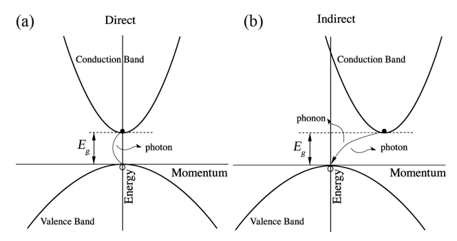
One dimensional band diagram having (a) direct and (b) indirect bandgaps.
These 2D plots are named 1D band diagram because direction of wave vector (or momentum) has been determined, however its magnitude is permitted to differ.
Conduction mechanism in Nano-structures
It is based on the naval surface warfare centre, Dahelgren division, has been interface research problems involved with the liquid dielectrics for 3 decades-
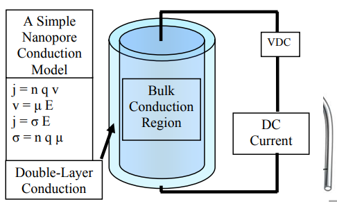
Water electrolytes modeling efforts have been progressed by traditional mechanism to include the charge injection. Currently work has been extended in the field of nano-technology and outcome in the measurement of the conductance by the water electrolyte wetted nano structured. The nano structures utilized were samples which were produced through the naval research laboratory and donated to NSWC. The validation key to the improved conduction double layer model is like reasonable values to the double layer improved and thickness mobility can count to the experimental observations. Those parameters is fitted by a trial and error procedure bounded through physical expectations to the water electrolytes. There are some expected boundaries involved-
Improved mobility limit equal to the ratio of dielectric constant in bulk which in the double layer. In practical this consider less than a factor of the 78 at the room temperature, however since dielectric constant of double layer is mostly calculated between 2 and 6, and the upper limit would better as above 40.
Double layer thickness limit to some of the multiple of Debye length in the water electrolyte, that is 3.033nm at the room temperature in the 0.01M NaCl.

With the ΛD = Debye length
ε = water dielectric constant, at room temperature of the 25
k = Boltzmann constant = 1.380658 x 10⁻²³ J/K
T = temperature in K, room temperature = 298.15K
e =electronic charge, 1.60217733 x 10⁻¹⁹ coulombs
Zi = ith conducting ion valence in the electrolyte water
Ni= ith conducting ion number density in the electrolyte water, this is in the terms of the ions number per cubic meter.
For calculating this we assumed to be 4 conducting ions in electrolyte- Na+, Cl-, H3O+ and OH-.
Even though mobilities of the all are order-of- magnitude, the hydronium number density and hydroxyl ions are 5 order of the magnitude less than chlorine and sodium ion for 0.01M salt. So the conductance is controlled by the chlorine and sodium.
Analysis
Below figure shows 2 experimental data curves as well as 2 theoretical calculations. The experiment data curves are not overlap and provide a good indication of the tough of the measurement. Previously described, AFM tip should be positioned across one of the 150-nm, water electrolyte filled up nanopores and held here while a slow, semi-DC sweep voltage and corresponding current measurement is made by the tip. When the tip may be drifting, and this is the case which the water is evaporating. Both these phenomena influence current measurement. Moreover 2 curves are not symmetric approximate 0 volt, this mean which are some another voltage possible present for example electrochemical mismatch between platinum coated silicon tip and copper grounding plate. It is surprising which the data reflect degree uncertainty.
In the structure of carbon nanostructures involves different type of low dimensional carbon allotropes including the carbon black, fullerene, carbon fiber, graphene and carbon nanotubes (CNTs). Graphene and CNTs have unique properties. CNTs have great mechanic properties and these are the strongest one.
s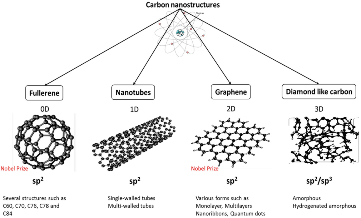
Concepts
1970- Osawa, a molecule is made up from SP2 hybridized carbons have a soccer type structure.
1973- Gal’pern and Bochvar, provide C20 and C60 structures and their properties.
1985- Kroto, this is a concept of the experiment with the vaporized carbon.
Several nano carbon structures
Fullerene
This is the allotrope of carbon whose molecule keeps of the carbon atoms which is connected through double and single bonds, therefore to from a partially closed mesh with the fused rings of 5 to 7 atoms. And the molecule may be ellipsoid, hollow sphere, tube or many other sizes and shapes.
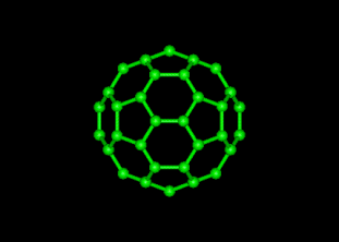
The explained structure for the C, a “truncated icosahedrons”, is extracted from an icosahedron through truncating or “shipping off” every of the 12 vertices. Every vertex is replaced through 5 membered rings, pentagon. This snipping procedure also changes each of 20 former triangular face into the 6 mentioned rings hexagons.
Nano-tubes
There are many carbon nanotubes applications and properties that take complete benefits of the CNTs features like ratio, thermal conductivity, electrical mechanical strength. The kinds of the carbon nanotubes are crucial mentioned to as single walled carbon Nanotubes and multi walled carbon Nanotubes.
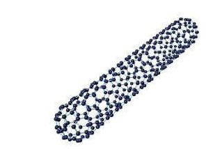
Single walled double walled carbon nanotubes molecular structure
Carbon nanotubes properties
Electrical conductivity
CNTs with the specific combinations of the N and M (structural parameters indicating how much nanotube is twisted) can be higher conducting and can be metallic. Its conductivity has been display to be chirality function ( twist degree), their diameter. CNTs can be either semi conducting or metallic in electrical behavior.
Strength and elasticity
Single sheet carbon atoms (graphene) of the form of graphite a planar honeycomb lattice, in that every atom are connected by a chemical bond to three neighboring atoms. Due to these strong bonds, basal plane elastic modulus of the graphite is one of the biggest of nay known materials.
Thermal conductivity and expansion
A new research indicates that CNTs may be the good heat conducting material, which ahs man ever known. SWNTs ultra-small have been shown to the exhibit superconductivity below 200k. This research suggest which exotic strands, already heralded their unparallel strength and unique ability to acquire electrical properties of the either semiconductor or the good metals.
Electron emission
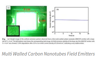
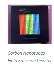
Results of the field emission from the electrons tunneling from a metal tip into the vacuum, under the application of the strong electric field. The high aspect ratio and small diameter of the CNTs is too favorable for the field emission. Even though for the moderate voltages, a strong electric field makes at free end of the supported CNTs cause of their sharpness.
High aspect ratio
CNTs depicts a too high aspect ratio, small conductive additive for the plastics of the all kinds. Its high aspects ratio means which a lower concentration of the CNTs is required which is compared to another conductive additives to get the similar electrical conductivity.
Carbon has four electrons in its outermost shell. So, this can form 4 covalent bonds with another molecules or atoms. The easiest organic carbon molecule is the methane (CH4), in these four hydrogen atoms bound to the carbon atom. But the structures which are more tough are made utilizing the carbon.
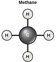
Carbon is found in many various compounds. It is in also food which is eaten, clothes, cosmetics which is utilize and the gasoline which fuels car. Carbon is too specific element because it plays the role in chemistry life.
In the chemistry, a cluster atom is a band of bound atoms or the molecule which is intermediate in size between an easy molecule and nano particle, which is up to a few nanometers (nm) in the diameter. Micro cluster term is utilized for band with up to the couple dozen atoms.
Carbon nanotube has been used in the construction of the body armor. These have the extraordinary strength of the nanotube utilized the thermal conductors and also have the unique properties. The nanotubes structures are belonging from fullerene family, that also involves the spherical Buckyball.
A carbon nanotube is made from the carbon, this is the tube-shaped material and nanometer scale is utilized to measuring its diameters.
Types of the carbon nano tubes
- Single walled nanotubes (SWNTs)
- Multi-walled nanotube
Applications
Cancer treatment
Carbon nanotubes are utilized in cancer treatment. Cancer is most ravaging diseases which approximately more than 10 million new patients are found every year from the various countries. Current cancer treatment methods like surgery, radiation and chemotherapy which successful in the many cases. These proper methods are destroying healthy cells and reason of the toxicity to the cancer patient.
In modern drug delivery systems, there are CNT’s considered as the antitumor agents while conventional drug merged with in, then got improvement their chemotherapeutic impact. This has been found which paclitaxel loaded PEG, carbon nanotube sare encouraging for the cancer therapeutic 27.
Nanotubes provide aqueous solutions of the SWCNTs on the exposure to the radiofrequency field experiences the efficient heating. This quality has been got for a selective and noninvasive thermal destruction of the treatment for the human cancer cells with the too less impact or nontoxic effects to normal cells. Carbon nanotubes are capable of the leading to innovative suitable directions in therapeutic human cancer 28 cells.
Bio engineering
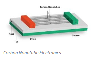
There are several applications which are proposed by the carbon nanotubes technology, like energy conversion and storage devices, high strength composite and conductive, sources, sensors and radiation, nanometer sized semiconductor devices and storage of hydrogen media 32-33. The concept of the MWCNT’s and SWCNT’s applied in academic and industrial for the research related activity. There are many various electronic device which is focused utilizing in the research activity like field emission of electron source for, flat panel displays, lamps and gas discharge tubes applicable for surge type protection, x-rays and microwave generations.
Cardiac autonomic regulation
There are several times single walled carbon nanotubes utilized in cardiac autonomic regulations. SWCNs are portion of the physiochemical property with the good element that may damage cardiovascular automatic dominant which proved after research in rats. Several times SWCNTs may change the baroreflex functions, then influencing autonomic cardiovascular handle regulation 34.
Platelet activation
The main application of SWNT is platelet activation in microcirculatory and macro thrombus formation. This is the platelet P-section expression way utilized in research on the platelet activation in micro, vitro and microcirculatory thrombus formation. This process has been reported which SWCNTs while injected into the anaesthzied rat, light induced thrombus formation is noted and then platelet activation found in 35.
Single electron transistor
A SET (single electron transistor) is a switching device which keeps of 2 tunnel junctions sharing the common electrode and develops utilize of controlled electron tunneling for the amplification of current. In single electron transistor technology is utilized is based on the theory of the quantum tunneling. Consider an essential element of the nanotechnology, SET give high operating speed and low consumption of power.
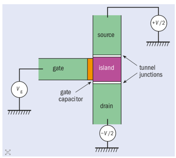
The SET can be shown as an electron box which has 2 separate junctions for exit and entrance of the single electrons. This can also be shown as the field effect transistor in that channel is exchanged by 2 tunnel junctions making a metallic island. And the volt is applied to the gate electrode influences amount of the energy required to modify number of electrons on island.
Principle
The SET transistor keeps of a gate electrode which electrostatically affects electrons travelling between drain and source electrodes. But SET electrons require to cross two tunnel junctions which form an isolated conducting electrode named island. Electrons are passing by the island charge and discharge it, and relative energy of the systems keeping 0 or 1 extra electron relies on gate voltage. At the low source –drain voltage, a current will be flow by SET transistor if these 2 charge configurations contains the similar energy.
Molecular machine
Molecular machine, nanomachine or nanite is the molecular element which generates quasi-mechanical results in the response to particular stimuli (input). In the field of biology macromolecular machines quickly done tasks which are important for life like DNA replication and ATP synthesis. An expression is generally applied to molecules which easily mimic functions which happen at macroscopic level. This term is common in the nanotechnology where the number of the highly typical molecular machine has been suggested which are goaled at the constructing molecular assembler.
Types of the molecular machines
Artificial molecular machines are listed below
Molecular motors
Molecular propeller
Molecular switch
Molecular shuttle
Nano car
Molecular balance
Molecular tweezers
Molecular sensor
Molecular logic gate
Molecular assembler
Molecular hinge
Biological is the most complex macro molecular machine.
BN nanotubes
BNNTs (boron nitride nanotubes) are a boron nitride polymorph. These were predicted in the year 1994 and discovered in the year 1995. They are similar with the carbon nanotubes in structure, that are cylinders with the sub-micrometer diameters and lengths of the micrometer, except which carbon atoms are alternately relieved through boron and nitrogen atoms. But, the properties of the BN nanotubes are too different, whereas carbon nanotubes can be semiconducting or metallic relying on rolling direction and radius, a BN nanotube are electrical insulator with the band gap of ~ 5.5 eV, fundamentally independent of tube morphology and chirality.
Synthesis and production
A well-developed technique of the carbon nanotube growth, like arc-discharge, chemical vapor deposition and laser ablation are utilized for the mass production of BN nanotube at a tens of grams scale. These can also be developed through ball milling of the amorphous boron, mixed with the catalyst (iron powder), under the NH3 atmosphere.
Properties and potential applications
Properties of the BN nanotubes like electrical and field emission can be tuned through doping with the gold atoms by gold sputtering on nanotubes.
BNNs are utilized in the cancer treatments due to their high stiffness and best chemical stability.
Nano wires
Nano wires just such as normal electrical wires which other than fact they are extremely small. These are made from the semiconducting and conducting materials such as silver, copper, gold , iron, zinc oxide and germanium. Also made form the carbon nanotubes.
Size of the nano wires are less than 100 nanometers and can be small as 3 nanometer . Due to the minute size of the nano wire, quantum mechanical effects become essential. “quantum wires” utilize quantum mechanics to generate wires with the range of the unique electrical properties.
Conductivity of nano wires
Edge effects, scattering caused and defects while width of nano wire is below free electron mean free path of the wire material, this means that nano wires are made from the metals can have been conductivity is much lower than that for bulk materials.
Applications
Small electronically circuits, transistors, advanced composite material, transistors, memory, quantum devices, biomolecular nano sensors, opto electronics, field emitters, and photon ballistic waveguides.
Nano materials used in batteries
Graphite and SEI
In lithium ion batteries anode is almost graphite. Anodes of graphite require to increase their stability of thermal and develop a higher power ability. Other electrolyte as well as graphite can undergo reactions which reduce electrolyte and develop a SEI, this effectively reduce the battery potential.
Grapheme and other carbon materials
Grapheme has been many utilizes in electromechanical systems like batteries. This offers high surface area and better conductivity. In present technology of lithium-ion battery, 2D graphite networks inhibit smooth lithium ion intercalation, lithium ions should travel around 2D graphite sheets to achieve electrolyte.
Titanium oxides
These oxides are another anode material which have been studied for their applications to the electric vehicles and grid energy storage. But, ionic capabilities and low electronic, as well as titanium high cost oxides have been proved material to unfavorable to another anode materials.
Silicon based anodes
These anodes have been study called for highest theoretical capacity which of the graphite. These have higher reactions rates with electrolyte, volumetric low capacity and an large volume expansion when cycling is done. But, current work has been performed to reduce volume expansion in the silicon-based anodes. By developing a conductive sphere carbon around silicon atom.
Photo voltaic cells
Silicon
CulnSe2, CIS(copper indium diselenide) thin layer present other type of the absorbent broadly utilized in the photovoltaic fact which their energy gap matches maximum solar spectra.
CdTe cadmium telluride is absorbent PV material with its bandgap of the 1.45 eV. This is utilized to combined to cadmium sulfide (CdS).
CdS (cadmium sulfide) is enter into the fabrication of solar cells which are based on the fluorine-doped tin oxide (FTO)/Au/TiO2/CdS polysulfide and photoanode electrolyte.
CdSe, the combination of the CdTe/CdSe shell/ core structure has the specifically to emit in near infrared region, that doesn’t exist to the CdTe or CdTe nanoparticles are taken apart.
Materials are used in supercapacitors
Various types of materials like activated template carbon, carbon, carbon nanotubes, graphene, carbon metal oxides, carbon nano materials and carbon nanofiber composites are utilized as the electrode for the supercapacitor.
Reference book
Benelmekki, M. Designing hybrid nanoparticles.
Kane, K. Metallic systems at the nano and micro scale.