Unit 4
Semiconductor Physics
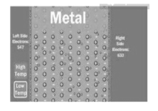
- This theory was developed by Lorentz and Drude in 1990.
- In metals there are large number of free electrons moving freely in all possible directions.
- The assumption is made that free electrons in metals behave like gas molecule obeying kinetic theory of gases.
- In metals electrons move randomly and collide with either +ve ions or free electrons accelerated in opposite direction to the applied.
|
|
Figure 1. Free electron theory
Quantum free electron theory
- In 1928, Sommerfeld developed a new theory applying quantum mechanical concepts and Fermi-Dirac statistics to the free electrons in the metal. This theory is called quantum free electron theory.
- Classical free electron theory permits all electrons to gain energy. But quantum free electron theory permits only a fraction of electrons to gain energy.
- In order to determine the actual number of electrons in a given energy range(dE), it is necessary to know the number of states(dNs) which have energy in that range. The number of states per unit energy range is called the density of states g(E).
Therefore, g(E) = dNs/dE. - According to Fermi-Dirac statistics, the probability that a particular energy state with energy E is occupied by an electron is given by,
f(E) = 1 / [1+e(E-EF/KT) ]
where EF is called Fermi level. Fermi level is the highest filled energy level at 0 K. - Energy corresponding to Fermi level is known as Fermi energy. Now the actual number of electrons present in the energy range dE,
dN = f(E) g(E)dE
Band theory of solids
- The atoms in the solid are very closely packed. The nucleus of an atom is so heavy that it is considered to be at rest and hence the characteristic of an atom are decided by the electrons.
- The electrons in an isolated atom have different and discrete amounts of energy according to their occupations in different shells and sub shells. These energy values are represented by sharp lines in an energy level diagram.
During the formation of a solid, energy levels of outer shell electrons got split up. As a result, closely packed energy levels are produced. - The collection of such a large number of energy levels is called energy band.
- The electrons in the outermost shell are called valence electrons. The band formed by a series of energy levels containing the valence electrons is known as valence band.
- The next higher permitted band in a solid is the conduction band. The electrons occupying this band are known as conduction electrons.
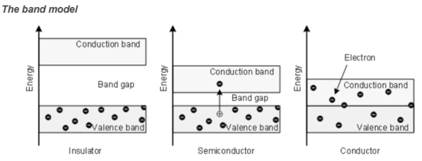
Conduction band valence band are separated by a gap known as forbidden energy gap. - No electrons can occupy energy levels in this band. When an electron in the valence band absorbs enough energy, it jumps across the forbidden energy gap and enters the conduction band, creating a positively charged hole in the valence band. The hole is basically the deficiency of an electron.
Classification of solids on the basis of energy bands
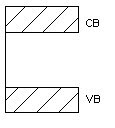
Insulator
Insulators are very poor conductors of electricity with resitivity ranging 103 – 1017 Ωm. In this case Eg ≈ 6eV.
For E.g. carbon.
|
Figure 2. Insulator
Semiconductor
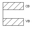
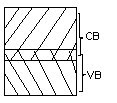
- A semiconductor material is one whose electrical properties lie between that of insulators and good conductors.
- Their forbidden band is small and resistivity ranges between 10-4to 103Ωm. Ge and Si are examples with forbidden energy gap 0.7eV and 1.1eV respectively.
- An appreciable number of electrons can be excited across the gap at room temperature.
- By adding impurities or by thermal excitation, we can increase the electrical conductivity in semiconductors
|
Figure 3. Semiconductor
Conductor
Here valence band and conduction band overlap and there is no forbidden energy gap. Resistivity ranges between 10-9 to 10-4 Ωm.
Here plenty of electrons are available for electrical conduction. The electrons from valence band can freely enter the conduction band.
|
Figure 4. Conductor
Intrinsic semiconductor
A pure semiconductor free from any impurity is called intrinsic semiconductor. Here charge carriers (electrons and holes) are created by thermal excitation.
- Si and Ge are examples.
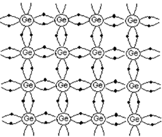
- Both Si and Ge are tetravalent that is each has four valence electrons in the outermost shell.
- Consider the case of Ge. It has a total of 32 electrons. Out of these 32 electrons, 28 are tightly bound to the nucleus, while the remaining 4 electrons valence electrons revolve in the outermost orbit.
- In a solid, each atom shares its 4 valence electrons with its nearest neighbors to form covalent bonds.The energy needed to liberate an electron from Ge atom is very small, of the order of 0.7 eV.
- Thus, even at room temperature, a few electrons can detach from its bonds by thermal excitation. When the electron escapes from the covalent bond, an empty space or a hole is created. The number of free electrons is always equal to the number of holes.
|
Figure 5. Intrinsic semiconductor
Extrinsic semiconductor
- Extrinsic semiconductors are formed by adding suitable impurities to the intrinsic semiconductor. This process of adding impurities is called doping.
- Doping increases the electrical conductivity in semiconductors. The added impurity is very small, of the order of one atom per million atoms of the pure semiconductor.
- The added impurity may be pentavalent or trivalent. Depending on the type of impurity added, the extrinsic semiconductors can be divided into two classes: n-type and p-type.
n-type semiconductor
- When pentavalent impurity is added to pure semiconductor, it results in n-type semiconductor.
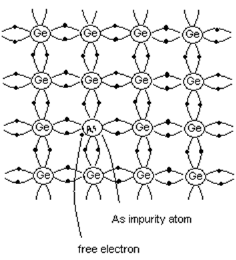
- Consider the case when pentavalent Arsenic is added to pure Ge crystal.
- As shown in the figure, four electrons of Arsenic atom form covalent bonds with the four valence electrons of neighboring atoms.
- The fifth electron of Arsenic atom is not covalently bonded, but it is loosely bound to the Arsenic atom.
- By increasing the thermal energy or by applying electric field, this electron can be easily excited from the valence band to the conduction band.
- Thus every Arsenic atom contributes one conduction electron without creating a positive hole.
- Hence Arsenic is called donor element since it donates free electrons. Since current carriers are negatively charged particles, this type of semiconductor is called n-type semiconductor.
|
Figure 6. Extrinsic semiconductor
p-type semiconductor
- When trivalent impurity is added to pure semiconductor, it results in p-type semiconductor.
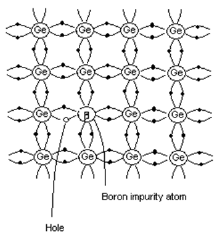
- Consider the case when trivalent Boron is added to pure Ge crystal.
- As shown in the figure, three valence electrons of Boron atom form covalent bonds with the three neighboring Ge atoms.
- There is a deficiency of one electron (hole) in the bonding with the fourth Ge atom. The Ge atom will steal an electron from the neighboring Ge atom to form a covalent bond.
- Due to this stealing action, a hole is created in the adjacent atom. This process continues.
- Impurity atoms that contribute hole in this manner are called acceptors.
- Since current carriers arepositively charged particles, this type of semiconductor is called p-type semiconductor.
|
Figure 7. p-type semiconductor
The mass of an electron in periodic intervals of crystal is different from free electron mass referred as effective mass.
According to de Broglie hypothesis a moving electron is associated with a wave. The velocity (v) is equal to the group velocity (vg) of the associated wave.
The group velocity is given by
vg = dw/dk -------------------------(1)
where w is angular frequency (2πv) and K is propagation vector of the wave.
In quantum mechanics, the energy E of an electron is given by
E = hw ----------------------------(2)
Substituting the value of w from (2) in (1) we get
vg = 1/h dE/dk --------------------------(3)
differentiating eq(3) w.r.t ‘t’ we get the acceleration of an electron as
a = 1/h d/dk (dE/dk) dk/dt
a = 1/h d2 E/dk2 .dk/dt -------------------------(4)
In 33quantum theory the momentum of an electron
p = hk----------------------------------(5)
Differentiating momentum with respect to t we get
dp/dt = h . dk/dt ------------------------------(6)
eq(4) and (6) reduces to
a = 1/ h2 (d 2 E / dk2 )dp/dt--------------------------(7)
Using Newton’s second law dp/dt = m x a and eq(6) reduces to
A = 1/ h2 ( d2 E / d k 2) m * a
m * = h 2 / ( d2 E / d k 2) ---------------------------(8)
This mass of an electron is called the effective mass of an electron denoted as m*.
The effective mass is determined by d2 E / d k 2.
From the band theory of solids we know that E is not proportional to K2 .
E = h 2 k 2 / 2 m *
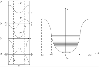
The variation of E with K is shown in figure. Using the type of variation of E with K from fig (a) . Plot v versus K as shown if fig(b).
At the bottom of the energy band the velocity of an electron is zero as the value of K increases , the velocity increases and attains maximum value at K =K 0 known as point of inflection on the E-K curve.
Beyond this point the velocity decreases and attains zero at K = π/a, which is the top of the band. The negative values of wave vector exhibit similar behavior.
The effective mass is represented as function f K in fig c.
|
Figure 8.
a) E-K diagram b) velocity versus K c) effective mass of an electron d) degree of freedom of an electron e) E-K diagram.
Density of states:
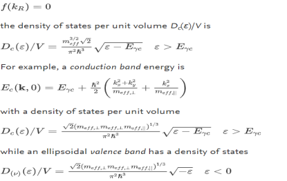
The density of states D(ε) is the number of electrons with a particular energy, say, ε. It is succinctly described by the Dirac δ-function expression:
(the factor 2 counts spin degeneracy). This, in turn, can be expressed as an effective mass. As a semiconductor example choose an isotropic conduction band in an effective mass approximation
where Eγc is the conduction band gap. For this isotropic band a density of states Dc(ε) is
--------------------------(3) Evaluating this by applying the δ-function identity
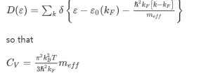
In terms of effective mass the density of states for the Fermi system is
|
|
|
|
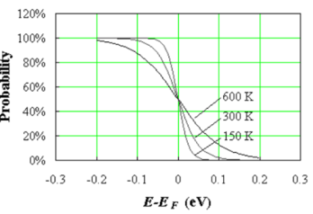
This function is plotted in Figure 1 at 150, 300 and 600 K.
|
|
Figure 9. Fermi function at three different temperatures
Conductors
Conductors are substances which have the property to pass different types of energy.
Metals
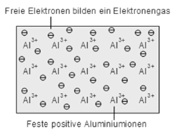
The conductivity of metals is based on the free electrons (so-called Fermi gas) due to the metal bonding. With low energy electrons become sufficiently detached from the atoms and a conductivity is achieved.
Metallic bonding: fixed ions and free valence electrons (Fermi gas)
|
Figure 10. Metallic bonding
The conductivity depends on the temperature. If the temperature rises, the metal atoms become stronger, so that the electrons are constrained in their movements.
Consequently, the resistance increases. The best conductors, are gold and silver.
The alternatives in the semiconductor technology for the wiring of the individual components of microchips are aluminum and copper.
Salts
In addition to metals, salts can also conduct electricity. There are no free electrons, so the conductivity depends on ions which can be solved when a salt is melting or dissolving, so that the ions are free to move.
Semiconductors
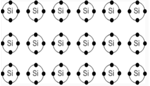
Semiconductors are solids whose conductivity lies between the conductivity of conductors and insulators. Due to exchange of electronsthat is to achieve the noble gas configuration semiconductors are arranged as lattice structure.
Unlike metals, the conductivity increases with increasing temperature. The increasing temperatures leads to broken bonds and free electrons are generated. At the location at which the electron was placed, a so-called defect electron ("hole") remains.
|
Figure 11. Silicon Lattice
|
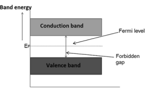
Figure 12.Position of Fermi level in intrinsic and extrinsic semiconductor
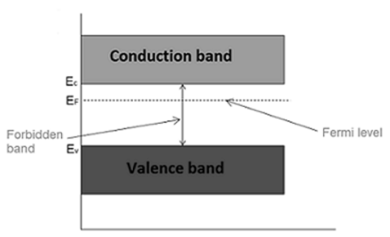
The probability of occupation of energy levels in valence band and conduction band is called Fermi level. At absolute zero temperature intrinsic semiconductor acts as perfect insulator. However as the temperature increases electrons and holes are generated.
In intrinsic or pure semiconductor, the number of holes in valence band is equal to the number of electrons in the conduction band.
Hence, the probability of occupation of energy levels in conduction band and valence band are equal. Therefore, the Fermi level for the intrinsic semiconductor lies in the middle of forbidden band.
|
Figure 13. Intrinsic semiconductor
Fermi level in the middle of forbidden band indicates equal concentration of free electrons and holes.
The hole-concentration in the valence band is given as
The electron-concentration in the conduction band is given as
|
Where KB is the Boltzmann constant
T is the absolute temperature of the intrinsic semiconductor
Nc is the effective density of states in the conduction band.
Nv is the effective density of states in the valence band.
The number of electrons in the conduction band is depends on effective density of states in the conduction band and the distance of Fermi level from the conduction band.
The number of holes in the valence band is depends on effective density of states in the valence band and the distance of Fermi level from the valence band.
For an intrinsic semiconductor, the electron-carrier concentration is equal to the hole-carrier concentration.
It can be written as
p = n = ni
Where P = hole-carrier concentration
n = electron-carrier concentration
and ni = intrinsic carrier concentration
The fermi level for intrinsic semiconductor is given as,

Where EF is the fermi level
EC is the conduction band
EV is the valence band
Therefore, the Fermi level in an intrinsic semiconductor lies in the middle of the forbidden gap.
Fermi level in extrinsic semiconductor
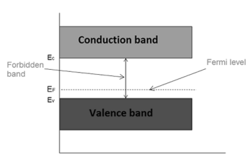
In extrinsic semiconductor, the number of electrons in the conduction band and the number of holes in the valence band are not equal. Hence, the probability of occupation of energy levels in conduction band and valence band are not equal. Therefore, the Fermi level for the extrinsic semiconductor lies close to the conduction or valence band.
Fermi level in n-type semiconductor
In n-type semiconductor pentavalent impurity is added. Each pentavalent impurity donates a free electron. The addition of pentavalent impurity creates large number of free electrons in the conduction band.
|
Figure 14. Extrinsic semiconductor
At room temperature, the number of electrons in the conduction band is greater than the number of holes in the valence band.
Hence, the probability of occupation of energy levels by the electrons in the conduction band is greater than the probability of occupation of energy levels by the holes in the valence band.
This probability of occupation of energy levels is represented in terms of Fermi level. Therefore, the Fermi level in the n-type semiconductor lies close to the conduction band.
The Fermi level for n-type semiconductor is given as
|
Where EF is the fermi level.
EC is the conduction band.
KB is the Boltzmann constant.
T is the absolute temperature.
NC is the effective density of states in the conduction band.
ND is the concentration of donar atoms.
Fermi level in p-type semiconductor
In p-type semiconductor trivalent impurity is added. Each trivalent impurity creates a hole in the valence band and ready to accept an electron. The addition of trivalent impurity creates large number of holes in the valence band.
|
Figure 15. p-type semiconductor
At room temperature, the number of holes in the valence band is greater than the number of electrons in the conduction band.
Hence, the probability of occupation of energy levels by the holes in the valence band is greater than the probability of occupation of energy levels by the electrons in the conduction band.
This probability of occupation of energy levels is represented in terms of Fermi level. Therefore, the Fermi level in the p-type semiconductor lies close to the valence band.
The Fermi level for p-type semiconductor is given as
|
Where NV is the effective density of states in the valence band.
NA is the concentration of acceptor atoms.
P-N Energy Bands
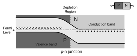
- At equilibrium the fermi levels match on the two sides of the pn-junctions.
- Electrons and holes reach an equilibrium at the junction and form a depletion region.
- The upward direction in the diagram represents increasing electron energy.
- which indicates the supply energy to get an electron to go up on the diagram, and supply energy to get a hole to go down.
|
Figure16.P-N Energy Bands
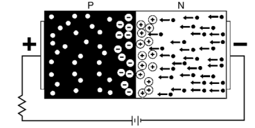
- To reverse bias the p-n junction the p-side is made more negative making it uphill for electrons moving across the junction.
- The conduction direction for electrons in the diagram is right to left and upward direction represents increase in electron energy.
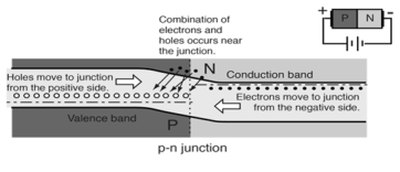
- When the p-n junction is forward biased the electrons in n-type material which have been elevated to conduction band have diffused across the junction and are at higher energy than holes in p-type material. These combine with holes which cause forward current through the junction.
|
Figure17.Forward Biased Conduction
- The forward current in a p-n junction when it is forward-biased involves electrons from the n-type material moving leftward across the junction and combining with holes in the p-type material.
- Electrons proceed further leftward by jumping from hole to hole, so the holes can be said to be moving to the right in this process.
|
Figure 18. Movement of electrons
Expression for barrier potential
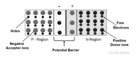
- When the P and N-type semiconductor material are placed together, the gradient of very large density charge carriers is created on both the P and N side region.
- The free electrons from N-side cross the region and start combining with the holes, leaving behind the immobile positive donor ions.
- Similarly, the holes of the P-region combine with the electrons of the N-region and leaving behind the negative acceptor ions.
|
Figure 19. Potential Barrier
- The process is continued until the P and N-region have enough charge carrier for opposing the electrons and holes respectively.
- The immobile ions (negative acceptor ions and positive donor ions) are concentrated between the N and P-region and create electric field which acts as a barrier between the flows of charges.
- The region is created because of the depleted ions, and hence it is called the depletion region.
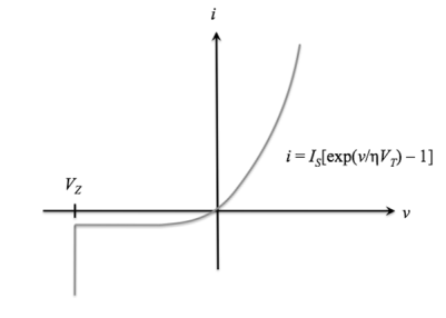
The ideal diode equation represents current flow through an ideal p-n junction diode as a function of applied voltage.
In realistic settings, current will deviate slightly from this ideal case. We know that ap-n junction diode creates the following current:
Under reverse bias, there is a small, constant reverse current, and under forward bias, there is a forward current that increases with voltage.
The current-voltage function (also called the "i-v characteristic") for an ideal diode is
i(v) = IS[exp(v /ηVT) - 1], v>VZ
whereISis the reverse saturation current,
v is the applied voltage
VT = T / 11,586 is the volt equivalent of temperature
η is the emission coefficient, which is 1 for germanium devices and 2 for silicon devices.
i is defined as positive when flowing from p to n. This is also called the Shockley ideal diode equation or the diode law.
For v ≤ VZ, the diode is in breakdown and the ideal diode equation no longer applies;
for v ≤ VZ, i = -∞. The ideal diode i-v characteristic curve is shown below:
|
Figure 20.Ideal diode equation
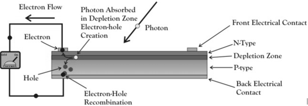
A solar cell is essential a PN junction with a large surface area. The N-type material is kept thin to allow light to pass through to the PN junction.
|
Figure 21. Solar cell
- Light travels in packets of energy called photons. The generation of electric current happens inside the depletion zone of the PN junction.
- The depletion region is the area around the PN junction where the electrons from the N-type silicon, have diffused into the holes of the P-type material.
- When a photon of light is absorbed by one of these atoms in the N-Type silicon it will dislodge an electron, creating a free electron and a hole.
- The free electron and hole have sufficient energy to jump out of the depletion zone.
- If a wire is connected from the cathode (N-type silicon) to the anode (P-type silicon) electrons will flow through the wire.
- The electron is attracted to the positive charge of the P-type material and travels through the external load (meter) creating a flow of electric current.
- The hole created by the dislodged electron is attracted to the negative charge of N-type material and migrates to the back electrical contact.
- As the electron enters the P-type silicon from the back electrical contact it combines with the hole restoring the electrical neutrality.
| |||||||||||||||||||||||||||||||||||||||||||||||||||||||||
|
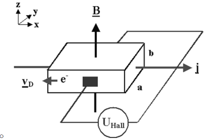
| The Hall effect describes what happens when current flows through a conducting material such as a metal or semiconductor ,when exposed to a magnetic field B. | |||||||||||||||||||||||||||||||||||||||||||||||||||||||
|
| ||||||||||||||||||||||||||||||||||||||||||||||||||||||||
|
|
Figure 22. Hall effect
both vectors.
|
|
| |||||||||||||||||||||||||||||||||||||||||||||||||||||
|
|
|
| ||||||||||||||||||||||||||||||||||||||||||||||||||||||
|
|
|
| ||||||||||||||||||||||||||||||||||||||||||||||||||||||
|
|
|
| ||||||||||||||||||||||||||||||||||||||||||||||||||||||
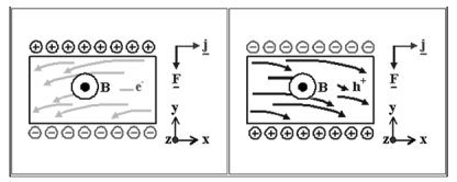
becomes charged as soon as the current is switched on.
| a
| ||||||||||||||||||||||||||||||||||||||||||||||||||||||||
| |||||||||||||||||||||||||||||||||||||||||||||||||||||||||
| |||||||||||||||||||||||||||||||||||||||||||||||||||||||||
Figure 23. Charge carriers
| |||||||||||||||||||||||||||||||||||||||||||||||||||||||||
| |||||||||||||||||||||||||||||||||||||||||||||||||||||||||
Reference: 1. Engineering Physics-Avadhanulu, Kshirsagar, S. Chand Publications 2. A textbook of optics- N Subrahmanyam and BriLal , S. Chand Publications 3. Engineering Physics- Gaur, Gupta, Dhanpat Rai and Sons Publications
| |||||||||||||||||||||||||||||||||||||||||||||||||||||||||
| |||||||||||||||||||||||||||||||||||||||||||||||||||||||||
| |||||||||||||||||||||||||||||||||||||||||||||||||||||||||
| |||||||||||||||||||||||||||||||||||||||||||||||||||||||||
| |||||||||||||||||||||||||||||||||||||||||||||||||||||||||
| |||||||||||||||||||||||||||||||||||||||||||||||||||||||||
| |||||||||||||||||||||||||||||||||||||||||||||||||||||||||
| |||||||||||||||||||||||||||||||||||||||||||||||||||||||||
