MICRO
Unit - 4Microwave Tubes Microwave tubes operate at frequencies from 300 MHz to 300 GHz with output power ranging from 10 mW to a few hundred watts. The operating principle of microwave tubes is based on velocity modulation of electrons. The velocity-modulation concept is used to prevent the problems caused due to transit-time effects that are encountered in conventional tubes. A long transit time is used very effectively in microwave tubes in the conversion of dc power to RF power. By using the resonant cavities in the microwave tubes, and the velocity modulation of electrons, the power can be interchanged. In conventional vacuum tubes, the modulation of electron beam can be done by altering the number of electrons. The microwave tubes are also called velocity-modulated tubes. In velocity-modulated tubes, the electron beam is formed by varying the velocity of electrons, in order to enable some electrons to move slowly and others to move rapidly through the inter-electrode space. Bunching of electrons occurs when the fast-moving electrons overtake the slowly moving electrons (which arrive before the fast-moving electrons). The microwave tubes are mainly classified into linear beam tubes (O-type) and crossed-field tubes (M-type). In linear beam tubes, the electron beam is parallel to both the electric and magnetic fields. However, in crossed-field tubes, the electric beam is perpendicular to both the electric and magnetic fields. 4.1 LIMITATIONS OF CONVENTIONAL TUBES AT MICROWAVE FREQUENCIESAt microwave frequencies above 1 GHz, the conventional tubes (triodes, tetrodes, and pentodes) are less useful signal sources. The limitations of conventional vacuum tubes at microwave frequencies are as follows,Effects of inter electrode capacitanceEffects due to lead inductance Effects due to transit time Limitation of gain bandwidth product.Inter-electrode Capacitance Effects :The inter-electrode capacitances in a vacuum tube produce capacitive reactance. At low and medium frequencies, the tube operation is not affected, even though the reactance value is very large. However, as the frequency increases, the reactance, XC = 1/2πfC, decreases and the output voltage decreases due to shunting effect. Since at higher frequencies, XC becomes almost a short, Cgp (grid-to-plate capacitance), Cgc (grid-to-cathode capacitance) and Cpc (plate-to-cathode capacitance) are the inter-electrode capacitance (IECs) that come into effect and are shown in the figure below,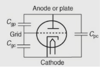 The inter-electrode capacitance can be reduced by decreasing the area of the electrodes, that is, by using smaller electrodes or by increasing the distance between electrodes. The relation for the capacitance is C = ɛ0εrA/d (1) where A = area of the electrode d = distance between electrodes ε0 = free space permittivity εr = relative permittivity Lead Inductance Effect :The lead inductance that appears at the connecting leads of the vacuum tube elements (e.g. cathode, plate and grid) is another limiting factor at higher frequencies. The three lead inductances that limit the performance of vacuum tube are: inductance at cathode (Lc), inductance at plate (Lp), and inductance at grid (Lg) as shown in the figure below,
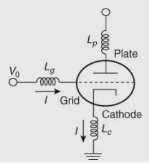 The main effects of the lead inductance at high frequencies are: they form unwanted tuned circuit by combining with the capacitance, which produce the parasitic oscillations they create an input impedance matching problem due to increase in the inductive reactance.The inductive reactance (XL =2πfL) in the connecting leads (wires or base pins) increases with the increase in frequency. Therefore, the input voltage drops across the lead inductance and only a fractional part of the applied input voltage reaches the terminals (e.g. grid), which decreases the gain of tube amplifier. Inductance is calculated by using the relation,
 (2)where A = area of the electrode l = length of the coil μ0 = permeability of free space = 4π × 10−7 H/m μr = relative permeability The effect of lead inductance can be minimized by decreasing L, that is, by using larger-sized short leads without base pins, and by increasing A and decreasing l. Due to this the power handling capability is reduced. Transit-time Effect:The time required for the electrons to travel from cathode to anode plate is called as transit time (τ). It is the main limitation caused at higher frequencies only. At low frequencies, transit time is not important and usually it is not considered as an affecting factor because the time period of the signal (T) is much greater than the transit time (T >> τ). On the other hand, at high frequencies, it is a considerable portion of the signal cycle and obstructs the efficiency because of the time period of the signal (T) is much smaller than the transit time (T << τ). In general, transit time may cause the reduction of efficiency if it exceeds 0.1 of the signal cycles. Transit time causes a phase shift between the plate current and the grid voltage resulting in reduction of efficiency. Transit time is the time taken by the electron to travel from cathode to anode and is given by,
 (3)Under equilibrium condition, static energy is equal to kinetic energy, that is,
 (4)Therefore,
 (5)where V0 = dc voltage d = distance between anode and cathode v0 = velocity of an electron e = charge of an electron m = mass of an electron To reduce the transit time, the separation between electrodes, “d” can be decreased (but this increases IEC), and the anode to cathode voltage can be increased (this cannot be increased indefinitely). Therefore, a trade-off between IEC and transit time is a must. Gain Bandwidth Product Limitation :Using a resonant circuit (LC tank circuit) across the load resistance (R) of an ordinary vacuum tube, maximum gain is achieved at a particular frequency as shown in the figure below,
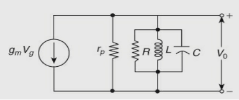 The gain bandwidth product is constant for all the vacuum tube amplifiers that employ resonant circuits and is given by
 (6) where Am = maximum voltage gains at resonance BW = bandwidth gm = transconductance C = the capacitance of the tank circuitWe note that the gain bandwidth product is independent of frequency. It depends on the tube parameter (gm) and the external capacitance (C) of the resonator. These resonant circuits can be used at low frequencies to achieve a higher gain, but at a narrower bandwidth. However, higher gain at broader bandwidth is desired at higher frequencies. This limitation can be overcome by using re-entrant cavities or slow-wave structures in place of the resonant circuits in microwave tubes. 4.2 CLASSIFICATION OF MICROWAVE TUBESMicrowave tubes are constructed so as to overcome the limitations of conventional and UHF tubes. The basic operating principle of microwave tubes involves the transfer of power from source of the dc voltage to the source of the ac voltage by means of a current density modulated electron beam. The same is achieved by accelerating electrons in a static field and retarding them in an ac field. The microwave tubes are mainly classified into linear beam tubes and crossed field tubes, and sub classified as shown in the figure below,
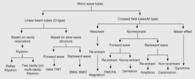 Linear beam tubes are often called O-type. In linear beam tubes, the electron beam travels along a straight path between the cathode and the collector. This electron beam is parallel to both the electric and magnetic fields. However, in crossed field tubes, the electron beam is perpendicular to both the electric and magnetic fields. Crossed-field tubes deals with the propagation of magnetic field waves, so they are known as M-type devices 4.3 RE-ENTRANT CAVITIESThe re-entrant cavities (also known as irregular-shaped resonators) are used in place of tuned circuits at microwave frequencies. These devices are easily incorporated into the microwave device structure. Below the microwave frequencies, the cavity resonator can be represented by lumped-constant resonant circuit. In order to maintain resonance at high operating frequency, the values of inductance and capacitance are decreased to a minimum by using a short wire. Hence, for use in klystron and other microwave tubes, the re-entrant cavities are designed. One more advantage of the re-entrant cavity is we can easily couple and take out the signal from these devices. In these devices the metallic boundaries are extended into interior of the cavity.
 Several types of re-entrant cavities are shown. One of the commonly used re-entrant cavities is the coaxial cavity as shown below,
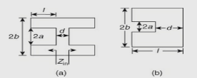
 4.4 VELOCITY MODULATIONVelocity modulation is defined as the variation in the velocity of a beam of electrons caused by the alternate speeding up and slowing down of the electrons in the beam. This variation is usually caused by a voltage signal applied between the grids through which the beam must pass. The direction of the electron beam and the static electrical field goes to each other parallelly into linear beam tubes. In other words, velocity modulation is the modification of the velocity of a stream of electrons by imparting alternate accelerations and decelerations to the electrons in such a way that they are caused to bunch together with the result that each bunch causes a cycle of current as it passes an output electrode. 4.5 LINEAR BEAM (O TYPE) TUBESAt present, the most important microwave tubes are the linear beam tubes. There are two basic types of linear beam tubes. One type of tube uses electromagnetic cavities, and the other type of tubes use slow-wave structure. Both types of tubes use an electron beam. As the name implies, in a linear beam tube, the electron beam and the circuit elements with which it interacts are arranged linearly. A simple schematic of a linear beam tube is shown in the figure,
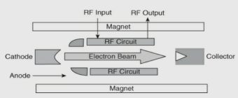 The electrons which are accelerated by the anode voltage possesses kinetic energy and this kinetic energy is calculated by using anode voltage. The applied RF input when interacts with the electron beam, a small part of kinetic energy that is present in it gets converted into microwave energy. At the RF output port, the microwave energy is extracted, and the remaining portion of electron beam is dissipated in the form of heat from the tube or it is sent back to the collector. As the electrons in the electron beam tends to repel each other, a magnetic field, is focused on the electrons as a beam going from the cathode to the collector. The magnetic field is generated either by an electromagnet or permanent magnets.Klystrons: Klystrons have high peak power, high average power, good efficiency, high gain, and low spurious signals. The working principle of klystron is based on velocity and density modulation. The resonant cavities are used to produce the bunching effect. The klystron is basically a vacuum electron device and it may be an oscillator or an amplifier since it is used for transforming DC energy into RF energy. In a klystron, the signal and the electron beam interact at a very short range. Therefore, a strong electrostatic field is required for efficient operation of the klystron. When the space charge in the beam decreases, then the klystron’s efficiency increases. By changing the velocity of an electron beam, the transit-time effect is utilized by the klystrons. Two-cavity or multi-cavity klystron: It is used as a low-power microwave amplifier. Reflex klystron: It is used as a low-power microwave oscillator. 4.6 TWO-CAVITY KLYSTRON AMPLIFIERThe two-cavity klystron is a widely used microwave amplifier that is operated by the principles of velocity and current modulation. In a two cavity-klystron amplifier, a high-velocity electron beam is produced, focused, and made to travel along a glass tube, a field-free drift space, and an output cavity (catcher) to a collector electrode/anode. The anode is maintained at a positive potential with respect to the cathode. Electrons from the cathode start drifting with constant velocity after being accelerated by a DC voltage. When the electrons pass through a pair of narrowly spaced grids, their velocity is modulated by a sinusoidal RF signal.Structure of Two-Cavity Klystron :The construction and essential components of a two-cavity klystron are shown in the figure below. It consists of a (i) cathode-anode configuration (i.e. electron gun) to produce an accelerated electron beam; (ii) a buncher (input) cavity; (iii) a catcher (output) cavity; (iv) field-free drift space between input and output cavities; and (v) a collector.
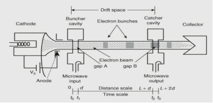 Electrons emitted by the cathode are focused by one or more focusing electrodes placed in front of the cathode. The electron beam then passes through the buncher and catcher cavities and finally reaches the collector. By using coupling loop, the RF power can be coupled through the buncher and catcher cavities.Velocity-modulation Process and Applegate DiagramThe velocity-modulation principle and operation of the klystron is explained by using the Applegate diagram as shown in the figure below. Assume a condition when there is no voltage across the gap A, and the electrons that pass-through gap A are unaffected and continue to the collector with the same velocities which they had before approaching the gap. If input is given to the buncher cavity, then the electrons which pass through this cavity are affected by the voltage depending on the variations of the voltage. Consider the instant when the electron passes through the gap A when the voltage across gap A is zero and is going positive. At this instant, the electric field across gap A is zero, and an electron that passes through gap A is unaffected by the input signal.
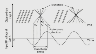 Let this electron be called the reference electron (re), which travels with an unchanged velocity given by,
 As shown in the figure, a late electron le passing the gap A slightly later than re is accelerated by the new positive voltage whose velocity (v) is greater than (v0) across gap A. This electron will catch up with the reference electron re and the early electron ee that was retarded by the negative voltage whose velocity (v) is less than (v0). As a result of these actions, the average velocity of electrons with which they leave the grid gap is similar to that with which they enter. While travelling through the drift region, the beam undergoes density modulation. The density of electrons passing the gap B vary cyclically with time, that is, the electron beam contains an ac current and is current modulated. The drift space converts the velocity modulation into current modulation. Bunching occurs only once for the cycle centered around the reference electron. With a proper design, a little RF power applied to the buncher cavity results in large beam currents at the catcher cavity with a considerable power gain. 4.7 REFLEX KLYSTRONFor applications which require variable frequency, Reflex klystron is used. It is a single cavity variable frequency microwave generator of low power and low efficiency. If a fraction of the output power is fed back to the input cavity and if the loop gain has a magnitude of unity with a phase shift which is a multiple of 2π, the klystron will oscillate. It produces an output power in the range of 10–500 mW and a frequency in the range of 1 to 25 GHz. This type is widely used in the laboratory for microwave measurements.The schematic diagram of a simple Reflex klystron is shown in the figure,
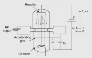 An electron gun, a filament surrounded by a cathode, an accelerating grid at cathode potential, and a repeller constitute the setup. The electron beam is accelerated towards the anode cavity, which is velocity modulated after passing through the gap in the cavity. All the electrons that cross during the positive half cycle of the gap voltage get accelerated and those which cross during the negative half cycle get decelerated.t0 = time for electron entering cavity gap at x = 0 t1 = the same electron leaving cavity gap at x = l t2 = time for the same electron returned by retarding field x = l and collected on walls of the cavity.The velocity modulated electrons travel towards a repeller electrode which is at a high negative potential. The electrons never reach this electrode because of the negative field and are returned back towards the gap. Under suitable conditions, the electron gives more energy to the gap than they took from the gap on their forward journey and oscillations are sustained.Applegate Diagram and Principle of Working :The electrons, which are reflected due to negative potential at the repeller, enter the cavity which acts as a catcher for these reflected electrons. At the same time, the cavity acts as a buncher for the new electrons. Some of the electrons come together, forming a bunch after spending a different amount of time in the repeller region. This bunching process can be clearly explained in the Applegate diagram as shown in the figure,
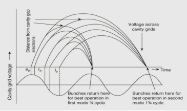 In the figure, the paths of electrons ee, re, and le are shown. Let me be a reference electron. It passes the gap towards the reflector, there is no effect of the gap voltage, and it is returned to the anode without reaching the reflector. Now consider an electron ee, which passes the gap slightly before re. If there is no gap voltage, early electron ee returns before re. However, RF voltage modulates the velocity of electrons. The electron ee is accelerated by the influence of the positive voltage, and it moves closer to the reflector than re. However, it is possible for re to catch up with the electron ee as it returns into the gap. In a similar manner, the late electron le leaving the gap slightly after the electron re is under the influence of the negative field, and, hence, it does not reach the reflector as close as the electron re. The electron le also catches up with ee and re electrons forming a bunch. Once the electrons leave the buncher and catcher gap, the velocity modulation is converted into current modulation. A reference electron is used to form one bunch per cycle of oscillations. For sustained oscillations, the energy is given by these bunches to the gap. An optimum value for time taken by the electrons for the round trip between the repeller space and the gap should be ensured for sustained oscillations. The transit time (τ ) corresponding to oscillation is given by,
 Where Tp is Time period of arriving electron bunches (or time period of RF signal); n is any integer (0, 1,.., n) that depends on repeller and anode voltages. Halfway between the catcher grids, maximum bunching occurs. The bunched electron beam should go through the retarding phase. In this retarding phase, the kinetic energy of the bunched electron beam is transferred to the field of the catcher cavity. The electrons finally come out from the catcher grids with a reduced velocity and are accumulated at the collector.Power Output and EfficiencyThe returning electron beam in the klystron should reach the cavity gap when the RF field in the cavity gap is maximum retarding so that oscillations can be produced with maximum energy. In this manner, there will be a maximum amount of kinetic energy transfer from the returning electrons to the cavity walls. The round-trip transit angle is given by,
 (1)This transit angle is with reference to the centre of bunch. Assuming V1 << V0, n = number of cycles (positive integer), and N = (n − 1/4) is the number of modes. When the electron beam enters the cavity again from the repeller region, its current modification can be determined in the similar manner as in a two-cavity klystron amplifier. The bunching parameters of a reflex klystron oscillator (X ′) and of a two-cavity klystron amplifier (X) are of opposite sign. The beam current also flows in negative Z-direction. Therefore, we can write the beam current of reflex oscillator as,
 (2)where θg << θ0, hence θg is neglected.The fundamental component of the current induced in the cavity by the modulated electron beam is given by,
 (3)The magnitude of the fundamental component is
 (4)The dc power supplied by the beam voltage V0 is Pdc = V0I0 (5)and the ac power delivered to the load is given by
 (6)We have,
 (7)Equation (7) is the bunching parameter of the reflex klystron oscillator.and

where,Vr = repeller voltage V0 = anode to cathode voltage Lr = distance between cavity gap and repellerv0 = 0.593 x From the above equations, we have, the ratio of V1 over V0 as expressed by
 (8)The maximum theoretical efficiency of a reflex klystron oscillator ranges from 20 to 30%. Oscillating Modes and Output Characteristics :The output frequency and the output power vary with the changes in repeller voltage for different modes. These modes are called mode curves. The oscillation frequency is determined by the frequency of resonance of the output cavity. This is called as electronic tuning range of reflex klystron. Therefore, the reflex klystron can be used as frequency modulated oscillator (voltage tunes oscillator). Operating characteristics the adjustment of repeller and anode voltage is in such a way that the bunch appears exactly at any of the positive maximum voltage of the RF signal, which is necessary for reflex klystron to undergo oscillations. The oscillations can be achieved only for some combination of anode and repeller voltages. The voltage or operating characteristics of reflex klystron are shown in the Figure 8.19 where the repeller and beam voltage combinations are represented in shaded portion. For a fixed frequency these diagrams are drawn. The pattern remains same for other frequencies, but there is a shift in the positions of regions because of variations in n. Large output power is obtained at lower modes which require high values of repeller and beam voltages. The modes corresponding to n = 2 or n = 3 are preferred usually. Electronic and Mechanical Tuning :Electronic tuning : The nature of the variation of output power and frequency by adjustment of the repeller voltage is called the electronic tuning. It can be measured by electronic tuning sensitivity (ETS). This can be determined by considering the slope of the frequency characteristics of the modes. The tuning range is about ±8 at the X-band and ± 80 MHz for sub-millimetre klystron.Mechanical tuning : In mechanical tuning, the effective capacitance and the resonant frequency of the klystron changes by changing the width of the cavity. But the output power remains unchanged in spite of the tuning. Mechanical tuning of reflex klystron may give a frequency variation that ranges from ±20 MHz at the X-band to ±4 GHz at 200 GHz. The frequency of resonance is mechanically adjusted by the following methods: By mechanically adjustable screws or the most popular method called post The Q of the cavity depends on its tuning by a screw or sliding piston. The current flows through the tuning elements. Because of the presence of these elements, the area becomes larger which decrease the Q. The resonant frequency is varied because of the introduction of dielectric materials. In another method there will be a wall which can be moved in or out slightly by an automatic screw, and it tightens or loosens small bellows. Sometimes this method can be used with the permanent cavities in reflex klystron which act as a form of limited frequency shifting. Thus, mechanical tuning can also be used to change the resonant frequency. 4.8 M-TYPE TUBESCrossed-field tubes are referred to as M-Type tubes, which deal with the propagation of waves in a magnetic field. In crossed field tubes both static electric and magnetic fields are present, and they are perpendicular to each other. The electron motion takes place in area where the fields are perpendicular to each other. These fields affect the RF behaviour of the electrons under RF fields. The magnetron is the most commonly used resonant crossed-field tube that is used in microwave circuits. Crossed-Field Effects :If both electric and magnetic fields are present, motion of electrons depends on the orientation of electric and magnetic fields. If electric and magnetic fields are in the same direction or the opposite direction, the magnetic field exerts no force on electrons. Therefore, electron motion depends only on the electric field as shown in the figure. Example: linear beam tubes. If electric and magnetic fields perpendicular to each other, electron motion depends on both electric and magnetic fields, this type of field is called cross field. In crossed-field tubes, the electrons emitted by the cathode are accelerated by the electric field, and the motion of electrons is perpendicular to both fields as is indicated in the figure. Analysing the operation of crossed field tube, consider that an RF field is applied to the anode circuit. During the retarding field, electrons which enter the field at this point are decelerated by the field and loose some of their energy to the RF field. Hence the electron velocity decreases. Now these electrons with less velocity will travel into the dc electric field, a far enough distance, they will retain their earlier velocity at the end of the field.
  The presence of cross field interactions makes the electrons to give up some of its energy to the RF field. Only those electrons which have given sufficient energy to the RF field can only be eligible to travel to the anode end. Hence this phenomenon makes M-type devices relatively efficient devices. On the other hand, when an electron enters into the circuit at the time of accelerating fields, it receives energy from RF fields which are in turn are accelerated or returned towards cathode. This phenomenon produces heat in the cathode and in turn reduces efficiency of the device. 4.9 MAGNETRONSThe magnetron is a crossed field device, in which electric field and magnetic field are produced in a direction perpendicular to each other, in a way to cross each other. Therefore, the flow of electrons is perpendicular to both the fields. In magnetrons anode and cathode are concentric and cylindrical type structures. The magnetic field causes the electrons that are emitted from the cathode to move in curved paths. Magnetrons use various shapes of cavities to build oscillations and power.There are three basic types of magnetrons: Cyclotron-frequency magnetrons Negative-resistance (split-anode) magnetrons Cavity-type magnetrons Cyclotron-frequency magnetrons: Its principle of working is based on the synchronization between orbiting electrons in a magnetic field and a resonant circuit that is tuned to the cyclotron frequency. In this magnetron the ac component of electric field and the oscillations of electrons are parallel to the field. Negative-resistance (split-resistance) magnetrons: It uses the static negative resistance between two anode segments. In this operation when both segments are at the same potential, the magnetic field effects can only be sufficient to keep flow of electrons to reach anode. By connecting a resonant circuit between the two anode segments, we can obtain sustained oscillations.Travelling-wave magnetrons: These magnetrons provide oscillations of high peak power and peak power capability that is increased by about an order of magnitude to 100 kW. The operating frequency of negative resistance magnetron is generally below the microwave region. In the case of cyclotron frequency magnetron, it operates at microwave frequency range, but it has low power output and efficiency (γ = 10% − split anode type, 1% single anode type). Since the efficiency is very low in the first two types, they are not dealt in this chapter. In general, travelling wave magnetrons uses cavity resonators.8-cavity Cylindrical MagnetronCavity magnetron is a high-power microwave oscillator with high efficiency. The operating principle of this device is interaction of electrons with the perpendicularly oriented electric and magnetic fields. An 8-cavity cylindrical magnetron is shown in Figure (a). It is a diode with eight re-entrant cavities and is concentric with an oxide-coated cathode. A permanent magnet was used for applying a magnetic field that is parallel to the cathode surface as shown in Figure (c). A cavity magnetron is usually of a cylindrical configuration with a thick cylindrical cathode at the centre and a co-axial cylindrical block of copper as anode as shown in Figure (b). In the anode block, a number of holes and slots act as resonant anode cavities. The electric field due to DC voltage applied between anode and cathode is radial, whereas the magnetic field produced by a permanent magnet is axial. When DC voltage and magnetic field are adjusted properly, due to the magnetic field, the electrons follow curved cycloidal paths in the cathode to anode interaction space. The electric field in this resonant oscillator can be resolved into two components i.e., alternating current field, direct current fields. In ac fields, it is undesirable effect for the electrons to take the energy from the ac fields. The RF oscillations which are induced at the anode block (cavity tank circuits) due to noise transients affects the dc field to extend radially between adjacent anode segments. Cloud of electrons will be formed around the cathode due to DC voltage (or thermionic emission). The energy has to be given to the inputs in the correct phase, in order to not to disturb the sustained oscillations in the resonant circuit, that is, for this, the anode DC voltage should be adjusted so that the average rotational velocity of electrons coincides with ϕ of gap voltage at various gaps.
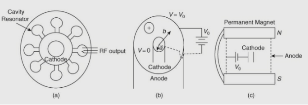 The heated cathode is a source of electrons in a magnetron. The cavity magnetron consists of 8 cavities that are tightly coupled to each other. If we consider the case of N cavity magnetron it will have N modes of operation. Each mode of operation will be distinctively characterised by, “frequency and phase of oscillation”, which are relative to next cavities. Sufficient care has to be taken while considering these combinations for a given mode so that it is self-consistent. That is the total phase shift produced by this system is 2nπ, n is an integer. The minimum phase shift should be 45° (45 × 8 = 360°). The relative phase change, ϕv of the electric field across the adjacent cavities can be given as,
 where
where
 That is, N/2 mode of resonance can exist only in resonator systems that have an even number of resonators. If n = N/2, ϕv = π. Since the phase angle of π radians is in the N/2 mode, this mode of resonance is called the π-mode. If n = 0, ϕv = 0, this mode is the zero mode; that is, there will be no RF electric field between the anode and cathode (called the fringing field) and it will be of no use in magnetron operations. To have an in-depth analysis of operation of cavity magnetron in which the RF field is applied in presence of perpendicularly oriented electric and magnetic fields, let us clearly understand that the incidence of electron in the EMF field. Electron trajectories at various magnetic fields: Comparing the magnitude of electric and magnetic fields, we can understand the trajectory of an electron coming from cathode, moving towards anode takes different paths through the interaction space. Electron trajectories at various magnetic fields V0 are present.If B = 0, electrons emitted from the cathode move along the radial direction
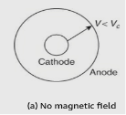 When a small B is applied (at a perpendicular to radial electric field), electron trajectories bend and follow a curved path. The radius of the curved path is directly proportional to the electron velocity and inversely proportional to the magnetic field strength.
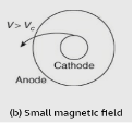 The magnetic field required to return electrons to the cathode while just grazing the surface of the anode is called the critical magnetic field (Bc) and is also known as the cut-off magnetic field. Under this condition, the motion of electrons is shown in the figure below,
 If the magnetic field is made larger than the critical field (B > Bc), the electrons travel with a greater velocity and may return to the cathode quite faster; these electrons may cause back heating of the cathode. To disallow this back heating of cathode we have to switch off the heater supply after oscillation. The equation of the cut-off magnetic field is given by
 where B = magnetic flux density a = cathode radius b = anode radiuse = charge of the electron m = mass of the electronConversely, the cut off voltage is given by
 Modes of Resonance and π Mode Operation :We have discussed the effect of electric and magnetic fields in the previous section when no RF field is applied. Let us assume RF oscillations are initiated and are maintained sustainably and assume that these oscillations are created by some noise which is transient in the magnetrons. The device is having high Q- cavity resonators. Now, we proceed to explain the mechanism by which the oscillations are sustained. Best results are obtained when n = 4, that is, the phase difference between adjacent cavities is π radians, and then there is a π mode of operation which is shown in the figure (a) below
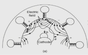 The electron “a” that is entering the interaction space during the decelerating field gives some of its energy to the RF field; therefore, its velocity decreases and it spends more time in interaction space during its long journey. In the same way, the electrons that are emitted a little later to be in the correct position move faster and try to catch up with electron “a”. The electrons that are emitted a little earlier than “a” slow down, and they fall back in step with electron “a”. All these favoured electrons come together, form electron bunches, and are confined to spokes or electron clouds. The process is called phase-focusing effect. The spokes so formed in the π mode rotate with an angular velocity that corresponds to two poles per cycle. The RF oscillations are sustained due to phase processing effect of the forward electrons which give enough energy to RF oscillations. The electron ‘b’ which is introduced during accelerated RF field takes energy from the oscillations. This results in increased velocity of electrons. Since the velocity is increased, the trajectory path of an electron bends more sharply, and it stays short time in the interaction space. Hence they are returned to the cathode early. These electrons are unfavoured electrons as they do not participate in bunching process rather, they are harmful in the sense that they cause back heating.Hull Cut-Off Voltage Equation :A cavity cylindrical magnetron is the most commonly used magnetron, because for a cross-field device the electric and magnetic fields are perpendicular to each other, and the path of the electrons in the presence of this cross-field is naturally parabolic. The equation for the hull cut-off voltage is given by
 where B = magnetic flux density a = cathode radius b = anode radiuse = charge of the electron m = mass of the electronThe Hull cut-off condition is obtained, under the condition that there is no RF field, which in turn defines anode voltage as a function of magnetic field. The magnetic field tends to prevent the flow of electrons to the anode. On the other hand, under right circumstances, the electrons leave the hub after getting interacted with the RF wave that is rotating about the cathode, and flow to the anode. It happens when the rotating speed of electrons is more than the RF wave. By interacting with the RF wave, the electrons speed is reduced to RF rotation rate. In this process the electrons amplify the wave and losses the energy.Hartree Condition :The Hull cut-off condition is obtained, under the condition that there is no RF field, which in turn defines anode voltage is a function of magnetic field. The magnetic field tend to prevent the flow of electrons to the anode. On the other hand, under right circumstances, the electrons leave the hub after getting interacted with the RF wave that is rotating about the cathode, and flow to the anode. It happens when the rotating speed of electrons is more than the RF wave. By interacting with the RF wave, the electrons speed is reduced to RF rotation rate. In this process the electrons amplify the wave and losses the energy. This happens when the anode voltage is such that the electrons are rotating faster than the RF wave. Therefore, velocity of electrons is reduced by giving up energy to the RF wave. The rate of rotation of electrons is reduced if the anode voltage is kept below the Hull cut-off voltage. Due to this, the electrons transfer less energy to the rotating wave. At a critical anode voltage, the rate of rotation of electrons and wave becomes equal. At this point the magnetron stops functioning as the electrons can no longer give up energy to the wave. The magnetron cannot work below that critical voltage as the rotation of the electrons is much slower than the RF wave. The critical voltage at which the magnetron stops functioning is called Hartree Voltage. The Hartree anode voltage equation is a function of the magnetic flux density and the spacing between the cathode and anode and is given by,
 where B = magnetic flux density d = spacing between anode and cathode η = circuit efficiency vm = mean spoke velocity va = Velocity of spoke at anode. 4.10 SLOW WAVE DEVICESTRAVELING-WAVE TUBETravelling-wave tube (TWT) is a broadband device. In this device the propagating speed of the wave is same as that of the electrons in the beam, and the microwave circuit is non resonant. The weak electric fields which are associated with the travelling wave produces a small amount of velocity modulation that initially effects the beam. Later on, this velocity modulation can be translated into current modulation same as in the klystron, where the RF current is induced in the circuit, causing the amplification.TWT is a broadband slow-wave device. Its operation is based on the interaction between the travelling wave structure and the electron beam. For extending the interaction of electron beam and RF field, it is compulsory to make sure that both of them travel in the same direction having virtually same velocity. TWT is a linear beam tube in which the interaction between the electron beam and the RF field is continuous over the full length of the tube.The travelling-wave tubes (TWTs) are commonly employed where a high power is required. The ordinary resonators, which are used in klystrons, cannot generate a large output, because the gain-bandwidth product is limited by the resonant circuit. The TWT uses slow-wave structures in its construction for obtaining large gain over a wide bandwidth. The special features of slow-wave structures can reduce the RF wave velocity in a certain direction so that the electron beam and signal wave can interact over a length. The phase velocity of a wave in ordinary waveguides is greater than the velocity of light in vacuum. In the operation of TWT, the electron beam should keep in step with the microwave signal. Since the electron beam can be accelerated only to velocities that are about a fraction of the velocity of light, a slow-wave structure should be incorporated in the microwave devices so that the phase velocity of the micro wave signal can keep pace with that of the electron beam. 4.11 Helix TWT: Construction and principle of operation, ApplicationsA helix is the most commonly used slow-wave structure. It consists of a thin ribbon of metal that is wound into a helical structure. A helix is also constructed by the use of a round wire that acts as a slow-wave structure.
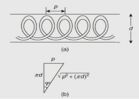
 From the above figure, the ratio of the phase velocity vp (phase velocity along the pitch ) and c (phase velocity along the coil) is given as,
 where, c = 3 × 10⁸ m/s is the velocity of light in free space p = helix pitch d = diameter of the helix Ψ = pitch angleMostly, the helix is surrounded by a dielectric filled cylinder. The TWT consists of an electron gun that is used to produce a narrow constant velocity electron beam. This electron beam is, in turn, passed through the centre of a long axial helix. Hence we use a magnetic field of high focusing capacity to avoid spreading and it will guide the wave through the centre of the helix. A helix is a loosely wound, thin conducting helical wire that acts as a slow-wave structure. The signal to be amplified is applied to the end of the helix that is adjacent to the electron gun. The amplified signal appears at the output or the other end of the helix under appropriate conditions. For the interaction between electronic beam and electric field, it is assumed that the axial space harmonic velocity should be synchronized with beam velocity. When the signal voltage is coupled into the helix, a force is acted upon the electrons due to the axial electric field. When we give an RF signal as input to the helix, part of RF signal’s electric field is in parallel with the direction of the electron beam and this causes an interaction between RF signal and the electronic beam. Bunching occurs due to interaction of electron beam and RF signal when the electrons in the beam are accelerated and travel faster than the RF signals.
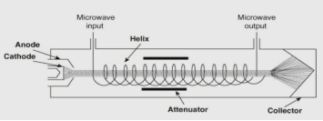
 The interaction between fields formed by these bunches and field from the RF signal produces amplification of RF signal. Each newly formed electron bunch adds a small amount of energy to the RF signal which is travelling in the helix as shown in the figure below. Now this merely amplified RF signal interacts with a dense electron bunch which again interacts with a denser electron bunch and gives additional energy to the RF signal. These types of interactions occur continuously over the full length of the helix. This energy is then coupled from the helix to the output side.
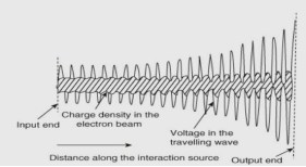
 Near the centre of the helix an attenuator is placed, and it reduces the waves travelling by the side of the helix to zero. Therefore, the reflected waves from the mismatched loads are prohibited from reaching the input and causing oscillation. A new electric field having same frequency can be induced by the bunched electrons from the attenuator. A new amplified microwave signal gets induced on the helix from this field. The analysis of motion of electrons in the helix type travelling wave tube can be done in terms of axial electric field. Applications of TWTLow-noise RF amplifier in broadband microwave receivers Repeater amplifier in wide band communication links and coaxial cables Due to long tube life, TWT is used as a power output tube in communication satellites.Continuous-wave high-power TWTs are used in troposcatter links. TWTA transmitters are extensively used in radars, particularly in airborne fire-control radar systems, and in electronic warfare and self-protection systems. Another major use of TWTs is in the electromagnetic compatibility (EMC) testing industry for immunity testing of electronic devices. Reference Books1. M. Kulkarni, “Microwave and Radar engineering”, 3rd edition, Umesh Publications2. ML Sisodia& GS Raghuvamshi, “Microwave Circuits and Passive Devices”Wiley, 19873. M L Sisodia& G S Raghuvanshi, “Basic Microwave Techniques and LaboratoryManual”, New Age International (P) Limited, Publishers.
 The inter-electrode capacitance can be reduced by decreasing the area of the electrodes, that is, by using smaller electrodes or by increasing the distance between electrodes. The relation for the capacitance is C = ɛ0εrA/d (1) where A = area of the electrode d = distance between electrodes ε0 = free space permittivity εr = relative permittivity Lead Inductance Effect :The lead inductance that appears at the connecting leads of the vacuum tube elements (e.g. cathode, plate and grid) is another limiting factor at higher frequencies. The three lead inductances that limit the performance of vacuum tube are: inductance at cathode (Lc), inductance at plate (Lp), and inductance at grid (Lg) as shown in the figure below,
 The main effects of the lead inductance at high frequencies are: they form unwanted tuned circuit by combining with the capacitance, which produce the parasitic oscillations they create an input impedance matching problem due to increase in the inductive reactance.The inductive reactance (XL =2πfL) in the connecting leads (wires or base pins) increases with the increase in frequency. Therefore, the input voltage drops across the lead inductance and only a fractional part of the applied input voltage reaches the terminals (e.g. grid), which decreases the gain of tube amplifier. Inductance is calculated by using the relation,
 (5)where V0 = dc voltage d = distance between anode and cathode v0 = velocity of an electron e = charge of an electron m = mass of an electron To reduce the transit time, the separation between electrodes, “d” can be decreased (but this increases IEC), and the anode to cathode voltage can be increased (this cannot be increased indefinitely). Therefore, a trade-off between IEC and transit time is a must. Gain Bandwidth Product Limitation :Using a resonant circuit (LC tank circuit) across the load resistance (R) of an ordinary vacuum tube, maximum gain is achieved at a particular frequency as shown in the figure below,
 The gain bandwidth product is constant for all the vacuum tube amplifiers that employ resonant circuits and is given by
 Linear beam tubes are often called O-type. In linear beam tubes, the electron beam travels along a straight path between the cathode and the collector. This electron beam is parallel to both the electric and magnetic fields. However, in crossed field tubes, the electron beam is perpendicular to both the electric and magnetic fields. Crossed-field tubes deals with the propagation of magnetic field waves, so they are known as M-type devices 4.3 RE-ENTRANT CAVITIESThe re-entrant cavities (also known as irregular-shaped resonators) are used in place of tuned circuits at microwave frequencies. These devices are easily incorporated into the microwave device structure. Below the microwave frequencies, the cavity resonator can be represented by lumped-constant resonant circuit. In order to maintain resonance at high operating frequency, the values of inductance and capacitance are decreased to a minimum by using a short wire. Hence, for use in klystron and other microwave tubes, the re-entrant cavities are designed. One more advantage of the re-entrant cavity is we can easily couple and take out the signal from these devices. In these devices the metallic boundaries are extended into interior of the cavity.
 Several types of re-entrant cavities are shown. One of the commonly used re-entrant cavities is the coaxial cavity as shown below,
 The electrons which are accelerated by the anode voltage possesses kinetic energy and this kinetic energy is calculated by using anode voltage. The applied RF input when interacts with the electron beam, a small part of kinetic energy that is present in it gets converted into microwave energy. At the RF output port, the microwave energy is extracted, and the remaining portion of electron beam is dissipated in the form of heat from the tube or it is sent back to the collector. As the electrons in the electron beam tends to repel each other, a magnetic field, is focused on the electrons as a beam going from the cathode to the collector. The magnetic field is generated either by an electromagnet or permanent magnets.Klystrons: Klystrons have high peak power, high average power, good efficiency, high gain, and low spurious signals. The working principle of klystron is based on velocity and density modulation. The resonant cavities are used to produce the bunching effect. The klystron is basically a vacuum electron device and it may be an oscillator or an amplifier since it is used for transforming DC energy into RF energy. In a klystron, the signal and the electron beam interact at a very short range. Therefore, a strong electrostatic field is required for efficient operation of the klystron. When the space charge in the beam decreases, then the klystron’s efficiency increases. By changing the velocity of an electron beam, the transit-time effect is utilized by the klystrons. Two-cavity or multi-cavity klystron: It is used as a low-power microwave amplifier. Reflex klystron: It is used as a low-power microwave oscillator. 4.6 TWO-CAVITY KLYSTRON AMPLIFIERThe two-cavity klystron is a widely used microwave amplifier that is operated by the principles of velocity and current modulation. In a two cavity-klystron amplifier, a high-velocity electron beam is produced, focused, and made to travel along a glass tube, a field-free drift space, and an output cavity (catcher) to a collector electrode/anode. The anode is maintained at a positive potential with respect to the cathode. Electrons from the cathode start drifting with constant velocity after being accelerated by a DC voltage. When the electrons pass through a pair of narrowly spaced grids, their velocity is modulated by a sinusoidal RF signal.Structure of Two-Cavity Klystron :The construction and essential components of a two-cavity klystron are shown in the figure below. It consists of a (i) cathode-anode configuration (i.e. electron gun) to produce an accelerated electron beam; (ii) a buncher (input) cavity; (iii) a catcher (output) cavity; (iv) field-free drift space between input and output cavities; and (v) a collector.
 Electrons emitted by the cathode are focused by one or more focusing electrodes placed in front of the cathode. The electron beam then passes through the buncher and catcher cavities and finally reaches the collector. By using coupling loop, the RF power can be coupled through the buncher and catcher cavities.Velocity-modulation Process and Applegate DiagramThe velocity-modulation principle and operation of the klystron is explained by using the Applegate diagram as shown in the figure below. Assume a condition when there is no voltage across the gap A, and the electrons that pass-through gap A are unaffected and continue to the collector with the same velocities which they had before approaching the gap. If input is given to the buncher cavity, then the electrons which pass through this cavity are affected by the voltage depending on the variations of the voltage. Consider the instant when the electron passes through the gap A when the voltage across gap A is zero and is going positive. At this instant, the electric field across gap A is zero, and an electron that passes through gap A is unaffected by the input signal.
 Let this electron be called the reference electron (re), which travels with an unchanged velocity given by,
 An electron gun, a filament surrounded by a cathode, an accelerating grid at cathode potential, and a repeller constitute the setup. The electron beam is accelerated towards the anode cavity, which is velocity modulated after passing through the gap in the cavity. All the electrons that cross during the positive half cycle of the gap voltage get accelerated and those which cross during the negative half cycle get decelerated.t0 = time for electron entering cavity gap at x = 0 t1 = the same electron leaving cavity gap at x = l t2 = time for the same electron returned by retarding field x = l and collected on walls of the cavity.The velocity modulated electrons travel towards a repeller electrode which is at a high negative potential. The electrons never reach this electrode because of the negative field and are returned back towards the gap. Under suitable conditions, the electron gives more energy to the gap than they took from the gap on their forward journey and oscillations are sustained.Applegate Diagram and Principle of Working :The electrons, which are reflected due to negative potential at the repeller, enter the cavity which acts as a catcher for these reflected electrons. At the same time, the cavity acts as a buncher for the new electrons. Some of the electrons come together, forming a bunch after spending a different amount of time in the repeller region. This bunching process can be clearly explained in the Applegate diagram as shown in the figure,
 In the figure, the paths of electrons ee, re, and le are shown. Let me be a reference electron. It passes the gap towards the reflector, there is no effect of the gap voltage, and it is returned to the anode without reaching the reflector. Now consider an electron ee, which passes the gap slightly before re. If there is no gap voltage, early electron ee returns before re. However, RF voltage modulates the velocity of electrons. The electron ee is accelerated by the influence of the positive voltage, and it moves closer to the reflector than re. However, it is possible for re to catch up with the electron ee as it returns into the gap. In a similar manner, the late electron le leaving the gap slightly after the electron re is under the influence of the negative field, and, hence, it does not reach the reflector as close as the electron re. The electron le also catches up with ee and re electrons forming a bunch. Once the electrons leave the buncher and catcher gap, the velocity modulation is converted into current modulation. A reference electron is used to form one bunch per cycle of oscillations. For sustained oscillations, the energy is given by these bunches to the gap. An optimum value for time taken by the electrons for the round trip between the repeller space and the gap should be ensured for sustained oscillations. The transit time (τ ) corresponding to oscillation is given by,
where,Vr = repeller voltage V0 = anode to cathode voltage Lr = distance between cavity gap and repellerv0 = 0.593 x
 The presence of cross field interactions makes the electrons to give up some of its energy to the RF field. Only those electrons which have given sufficient energy to the RF field can only be eligible to travel to the anode end. Hence this phenomenon makes M-type devices relatively efficient devices. On the other hand, when an electron enters into the circuit at the time of accelerating fields, it receives energy from RF fields which are in turn are accelerated or returned towards cathode. This phenomenon produces heat in the cathode and in turn reduces efficiency of the device. 4.9 MAGNETRONSThe magnetron is a crossed field device, in which electric field and magnetic field are produced in a direction perpendicular to each other, in a way to cross each other. Therefore, the flow of electrons is perpendicular to both the fields. In magnetrons anode and cathode are concentric and cylindrical type structures. The magnetic field causes the electrons that are emitted from the cathode to move in curved paths. Magnetrons use various shapes of cavities to build oscillations and power.There are three basic types of magnetrons: Cyclotron-frequency magnetrons Negative-resistance (split-anode) magnetrons Cavity-type magnetrons Cyclotron-frequency magnetrons: Its principle of working is based on the synchronization between orbiting electrons in a magnetic field and a resonant circuit that is tuned to the cyclotron frequency. In this magnetron the ac component of electric field and the oscillations of electrons are parallel to the field. Negative-resistance (split-resistance) magnetrons: It uses the static negative resistance between two anode segments. In this operation when both segments are at the same potential, the magnetic field effects can only be sufficient to keep flow of electrons to reach anode. By connecting a resonant circuit between the two anode segments, we can obtain sustained oscillations.Travelling-wave magnetrons: These magnetrons provide oscillations of high peak power and peak power capability that is increased by about an order of magnitude to 100 kW. The operating frequency of negative resistance magnetron is generally below the microwave region. In the case of cyclotron frequency magnetron, it operates at microwave frequency range, but it has low power output and efficiency (γ = 10% − split anode type, 1% single anode type). Since the efficiency is very low in the first two types, they are not dealt in this chapter. In general, travelling wave magnetrons uses cavity resonators.8-cavity Cylindrical MagnetronCavity magnetron is a high-power microwave oscillator with high efficiency. The operating principle of this device is interaction of electrons with the perpendicularly oriented electric and magnetic fields. An 8-cavity cylindrical magnetron is shown in Figure (a). It is a diode with eight re-entrant cavities and is concentric with an oxide-coated cathode. A permanent magnet was used for applying a magnetic field that is parallel to the cathode surface as shown in Figure (c). A cavity magnetron is usually of a cylindrical configuration with a thick cylindrical cathode at the centre and a co-axial cylindrical block of copper as anode as shown in Figure (b). In the anode block, a number of holes and slots act as resonant anode cavities. The electric field due to DC voltage applied between anode and cathode is radial, whereas the magnetic field produced by a permanent magnet is axial. When DC voltage and magnetic field are adjusted properly, due to the magnetic field, the electrons follow curved cycloidal paths in the cathode to anode interaction space. The electric field in this resonant oscillator can be resolved into two components i.e., alternating current field, direct current fields. In ac fields, it is undesirable effect for the electrons to take the energy from the ac fields. The RF oscillations which are induced at the anode block (cavity tank circuits) due to noise transients affects the dc field to extend radially between adjacent anode segments. Cloud of electrons will be formed around the cathode due to DC voltage (or thermionic emission). The energy has to be given to the inputs in the correct phase, in order to not to disturb the sustained oscillations in the resonant circuit, that is, for this, the anode DC voltage should be adjusted so that the average rotational velocity of electrons coincides with ϕ of gap voltage at various gaps.
 The heated cathode is a source of electrons in a magnetron. The cavity magnetron consists of 8 cavities that are tightly coupled to each other. If we consider the case of N cavity magnetron it will have N modes of operation. Each mode of operation will be distinctively characterised by, “frequency and phase of oscillation”, which are relative to next cavities. Sufficient care has to be taken while considering these combinations for a given mode so that it is self-consistent. That is the total phase shift produced by this system is 2nπ, n is an integer. The minimum phase shift should be 45° (45 × 8 = 360°). The relative phase change, ϕv of the electric field across the adjacent cavities can be given as,
 When a small B is applied (at a perpendicular to radial electric field), electron trajectories bend and follow a curved path. The radius of the curved path is directly proportional to the electron velocity and inversely proportional to the magnetic field strength.
 The magnetic field required to return electrons to the cathode while just grazing the surface of the anode is called the critical magnetic field (Bc) and is also known as the cut-off magnetic field. Under this condition, the motion of electrons is shown in the figure below,
 If the magnetic field is made larger than the critical field (B > Bc), the electrons travel with a greater velocity and may return to the cathode quite faster; these electrons may cause back heating of the cathode. To disallow this back heating of cathode we have to switch off the heater supply after oscillation. The equation of the cut-off magnetic field is given by
 where B = magnetic flux density a = cathode radius b = anode radiuse = charge of the electron m = mass of the electronConversely, the cut off voltage is given by
 The electron “a” that is entering the interaction space during the decelerating field gives some of its energy to the RF field; therefore, its velocity decreases and it spends more time in interaction space during its long journey. In the same way, the electrons that are emitted a little later to be in the correct position move faster and try to catch up with electron “a”. The electrons that are emitted a little earlier than “a” slow down, and they fall back in step with electron “a”. All these favoured electrons come together, form electron bunches, and are confined to spokes or electron clouds. The process is called phase-focusing effect. The spokes so formed in the π mode rotate with an angular velocity that corresponds to two poles per cycle. The RF oscillations are sustained due to phase processing effect of the forward electrons which give enough energy to RF oscillations. The electron ‘b’ which is introduced during accelerated RF field takes energy from the oscillations. This results in increased velocity of electrons. Since the velocity is increased, the trajectory path of an electron bends more sharply, and it stays short time in the interaction space. Hence they are returned to the cathode early. These electrons are unfavoured electrons as they do not participate in bunching process rather, they are harmful in the sense that they cause back heating.Hull Cut-Off Voltage Equation :A cavity cylindrical magnetron is the most commonly used magnetron, because for a cross-field device the electric and magnetic fields are perpendicular to each other, and the path of the electrons in the presence of this cross-field is naturally parabolic. The equation for the hull cut-off voltage is given by
 where B = magnetic flux density a = cathode radius b = anode radiuse = charge of the electron m = mass of the electronThe Hull cut-off condition is obtained, under the condition that there is no RF field, which in turn defines anode voltage as a function of magnetic field. The magnetic field tends to prevent the flow of electrons to the anode. On the other hand, under right circumstances, the electrons leave the hub after getting interacted with the RF wave that is rotating about the cathode, and flow to the anode. It happens when the rotating speed of electrons is more than the RF wave. By interacting with the RF wave, the electrons speed is reduced to RF rotation rate. In this process the electrons amplify the wave and losses the energy.Hartree Condition :The Hull cut-off condition is obtained, under the condition that there is no RF field, which in turn defines anode voltage is a function of magnetic field. The magnetic field tend to prevent the flow of electrons to the anode. On the other hand, under right circumstances, the electrons leave the hub after getting interacted with the RF wave that is rotating about the cathode, and flow to the anode. It happens when the rotating speed of electrons is more than the RF wave. By interacting with the RF wave, the electrons speed is reduced to RF rotation rate. In this process the electrons amplify the wave and losses the energy. This happens when the anode voltage is such that the electrons are rotating faster than the RF wave. Therefore, velocity of electrons is reduced by giving up energy to the RF wave. The rate of rotation of electrons is reduced if the anode voltage is kept below the Hull cut-off voltage. Due to this, the electrons transfer less energy to the rotating wave. At a critical anode voltage, the rate of rotation of electrons and wave becomes equal. At this point the magnetron stops functioning as the electrons can no longer give up energy to the wave. The magnetron cannot work below that critical voltage as the rotation of the electrons is much slower than the RF wave. The critical voltage at which the magnetron stops functioning is called Hartree Voltage. The Hartree anode voltage equation is a function of the magnetic flux density and the spacing between the cathode and anode and is given by,


0 matching results found
Browse by Topics