MICRO
Unit - 5MICROWAVE SOLID STATE DEVICES INTRODUCTIONBefore the 1960s, vacuum tube technology was widely used in electronics, which increased the size and cost of the entire system. Later, the development in semiconductor technology led to the growth of solid-state devices, which were more reliable and had a longer life. These devices generally require low power and are very compact and lighter in weight. In the recent past, tremendous research activities have taken place for the development of better, low-noise, high-frequency, and greater-bandwidth components to achieve lesser switching time and better performance characteristics. In this chapter, several microwave solid-state devices, including two terminal devices such as transferred electron devices (Gunn diodes), avalanche transit time devices (IMPATT, TRAPATT, and BARITT diodes), tunnel diodes, and three terminal devices such as bipolar junction transistors and field effect transistors (MESFETs and HEMTs).There are various microwave solid state devices which show negative resistance characteristics. The real part of their impedance is negative over a range of frequencies. In a positive resistance, the current through the resistor and the voltage across it are in phase. The voltage drop across positive resistance is positive, and the power that is given by the product of voltage (V) and current (I) is dissipated in the resistor. In a negative resistance, the current and voltage are out of phase by 180°. Therefore, the voltage drop across it is negative, and a negative power is generated by the power supply associated with the negative resistance. In other words, negative resistance generates or supplies power (e.g. active solid state devices) to the external circuits and positive resistance absorbs power (e.g. passive solid state devices). However, the reason for exhibiting negative resistance varies from one device to another. For instance, in tunnel diode the negative resistance is due to heavy doping where the majority carries tunnel through the thin barrier. In an IMPATT, it is due to delay, which causes the current to lag behind the voltage, whereas in TEDs, it is due to differential negative electron mobility characteristic in materials such as GaAs and InP. Solid-state devices can be classified into two categories depending on the number of terminals these device have. They are diodes and transistors. Depending on their principle of operation, the two terminal diodes are further classified as shown in the figure. Transferred Electron Devices (TED), tunnel diodes, and Avalanche Transit Time Devices (ATD) show negative resistance. The three terminal devices are also further divided into two types as shown in the figure. Microwave BJTs are bipolar devices, whereas microwave FETs are unipolar devices. 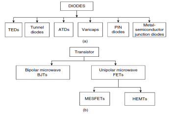 5.1 MICROWAVE BJTSA bipolar junction transistor operated in the microwave region is called a microwave BJT. The operation of the microwave BJT is similar to that of low-frequency transistors. However, the major differences are• GaAs is to be used instead of silicon, because the mobility of electrons is more in GaAs than in Si.• To minimize junction capacitance, the size of the device should be minimized.• The emitter forward resistance is to be minimized by reducing the thickness of the emitter and also by applying maximum possible forward voltage at the emitter junction.• The base transit time is to be reduced by minimizing its thickness and using a graded doping profile.In the analysis and designing of a circuit with microwave BJT, the following points should be considered:A much more complex equivalent circuit model as shown in the figure below is considered. This includes package parasitic capacitance, lead inductance, and resistance.
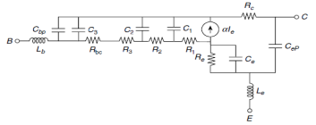 Equivalent circuit of microwave BJTCbp —base bond pad capacitanceCep —emitter bond pad capacitanceRbc —base contact resistanceRec —emitter contact resistanceR1, R2, R3 —base distributed resistanceC1, C2, C3 —collector base distributed capacitanceRe —dynamic emitter-base diode resistanceCe —emitter-base diode junction capacitanceRc —collector resistanceLb, Le — base and emitter bond wire inductances Construction: These are usually N-P-N type, because the electron mobility is higher than the hole mobility. The structure of a conventional Si homojunction N-P-N BJT is as shown in the figure below. N-P-N BJT is designed with planar shape as a double diffused epitaxial transistor.
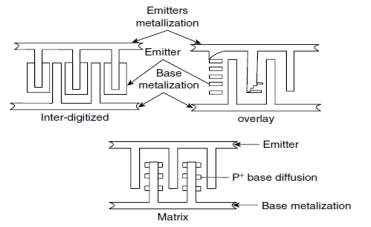
 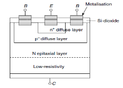 An N-type epitaxial layer, which acts as a collector, is grown on an N + substrate. An insulating layer of silicon dioxide is grown thermally over the epitaxial layer. The base and emitter layer are formed by diffusion or ion implantation. Proper care is to be taken during the whole process of microwave BJT fabrication so as to reduce package parasites considerably. Contacts are provided by means of openings in the oxide, and connections are made in parallel. The surface geometry of the microwave transistor can be any one of the following:(a) inter-digitized(b) overlay(c) matrixAll the three types are as shown in the figure below. In an inter-digitized geometry, a large number of metallized emitter strips alternating with metallized base strips are present as shown in the figure.This type is used for small signal and power transistors. The second one is the overlay geometry that has a large number of segmented emitters overlying a number of wide metal strips. The third is the matrix or mesh geometry that has an emitter which forms the grid, with the base filling the meshes of this grid with a P+ contact area in the middle of each mesh. Overlay and matrix structures are useful for power transistors.
  Operation of BJT: Microwave BJT behave very similarly to a low-frequency N-P-N bipolar transistor.In an N-P-N BJT, primarily, the collector-base and emitter-base junctions are reverse biased, consequent to the class C condition. The microwave frequency signal is applied between the emitter and base junction, this junction forward bias during the positive portion of the microwave signal. A pulse of current flows through the load connected in the collector circuit. In a proper-designed microwave BJT, the emitter current consists almost all of the electrons and is approximately equal to the collector current, while very small fraction of the emitter current is the base current.The mode mentioned just now is known as an active mode. There are two other operation modes.One is the cut-off mode, in which the emitter and collector junctions are reverse biased and the collector current is negligible, and another mode is the saturation mode, in which both the emitter and collector junctions are forward biased, resulting in a large collector current. Disadvantages: Microwave transistors also suffer from high-frequency limitations. The effects like transit time, inter electrode capacitance etc, come into view again at high frequencies. For example, due to the effect of the inter electrode capacitance high frequency response is limited which causes increase the complexity of the transistor. Lead inductance cause undesirable effect. Ideally, these effects should be kept lowest with appropriate selection of geometry and packaging of BJTs. In addition, they operate at lower frequencies than microwave field effect transistors (FETs). 5.2 MICROWAVE FETSMicrowave FET operates at higher frequencies than those of BJT. Basically, there are two kinds of microwave FETs. They are• Metal Semiconductor FET(MESFET)• Hetero structure FET(HFET)All the above kinds have a source, a drain, and a channel between them. The electric field across the channel can be changed to vary the conductivity of the device. A detailed discussion of MESFETs is given next. 5.3 MESFETConstructional features of a GaAs MESFET are as follows: Initially, a semi-insulating GaAs substrate is taken (To make it semi-insulating, GaAs is doped with chromium). Over that substrate, a thin active layer of N-type GaAs material is grown by ion implantation of donor atoms into the substrate.This active layer has a resistivity that is more than 107 ohm-cm. Three metal contacts for source, gate, and drain are made as shown in the figure. To reduce the contact resistance, the regions beneath the source and drain contacts are diffused with highly doped materials.
 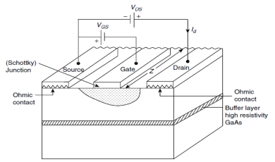 MESFET The channel region is a thin epitaxial N-type GaAs grown on a chromium-doped insulating GaAs substrate. The gate is not a simple P-N junction, but has a Schottky barrier metal contact. The Schottky barrier voltage partially depletes the thin channel under the gate as long as channel doping is in the order of a few 1017cm-3. The positive drain to source voltage will let the current flow through the device.Negative Vgs further reduces the drain to the source current. As VGS approaches the pinch-off voltage, IDS remains constant. The cut-off frequency of the device is given by,
  where is the carrier transit time that is obtained by dividing the length of channel l with the saturation velocity of electrons. The expression for pinch-off voltage is given by,
  a = channel heightɛs = semiconductor dielectric permittivityNd = Electron Concentration Applications:• They are used in various applications such as attenuators, mixers, oscillators, amplifiers, phase shifters, transfer switches, frequency multipliers, discriminators, and isolators.• They are used as power amplifiers 5.4 VARACTOR DIODEA varactor is a variable capacitance junction diode. These two terminal devices are also called varicaps or voltacaps. This is a special type of PN junction that is designed to operate in a microwave range. It works on the principle of voltage variable nature of the depletion capacitance. Working: In a PN junction, due to the density gradient, holes diffuse to the N region and electrons diffuse to the P region. This causes a few ions on either side of the junction to be depleted of mobile charges as shown in the figure below. This region is known as the depletion region or space charge region.
 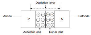 If a forward bias is applied, the carriers move toward the junction as shown in the figure below, which reduces the depletion width.
  If a reverse bias is applied, the carriers move away from the junction; as a result, the depletion width increases as shown in the figure below,
  The variation of width with voltage may be considered a capacitive effect with the depletion region as a dielectric, and P and N regions as parallel plates. This capacitance is known as transition capacitance or junction capacitance and is given by
  where,A is area of junctionW is depletion widthεs is permittivity Therefore, this capacitance is not constant, but depends on the magnitude of the applied bias. It is inversely proportional to the applied voltage
  Electronic symbol of varactor diode. 5.5 PIN DIODEIt is a variation of the conventional PN junction diode with a small layer between P and N layers. It consists of a layer of intrinsic semiconductors between two heavily doped P- and N-type semiconductors (Figure). The width of the intrinsic region may vary from 10 to 200 micro meters. This long intrinsic region makes the device capable of withstanding high breakdown voltages. The equivalent symbol of the PIN diode is shown in the figure below.
 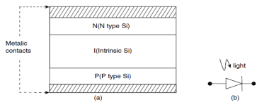 (a) PIN diode; (b) PIN diode symbol Principle of operation Under the no-bias condition, the I-region of a PIN diode has a very few charge carriers. Holes from the P region and electrons from the N region diffuse into the intrinsic region. The width of the space charge region is inversely proportional to impurity concentration. Therefore, the space charge regions of P and N are very narrow.When a reverse bias is applied, thermally generated electrons move toward the N-region, and thermally generated holes move toward the P-region; as a result of this, a small electron-hole current flows through the device. The space charge region extends into the intrinsic region and almost covers it such that the depletion width (wd) and the width of the intrinsic layer (wI) are equal. The junction capacitance is given by,
  where A is the effective area, and εs is the permittivity of the semiconductor. Therefore, the large width of the intrinsic region makes the junction capacitance less, making it suitable for switching applications.When a forward bias is applied, a large number of holes from the P-region and electrons from the N-region enter the intrinsic region. If the width of the intrinsic region is smaller than the diffusion length of electrons, injected carriers do not combine immediately but they remain in the intrinsic region. This reduces the resistance of the intrinsic layer. If the forward bias is increased further, more and more carriers are injected into the I-region, further reducing its resistance. This is provided by the doping which is sufficient enough to supply the carriers. Hence, the resistance of the I layer can be determined by controlling the forward bias. This is known as conductivity modulation.The PIN diode can be used as a microwave device only above 200 MHz. At low frequencies, the diffusion length of carriers is small. Therefore, the carriers recombine in the intrinsic layer, and the diode behaves similar to an ordinary PN diode. Applications• It is used as a limiter.• As a modulator• It is used as a dc-operate attenuator in TV tuners, antenna distribution amplifiers, and so on.• Provides isolation in certain applications• Used as a switch• Used as a phase shifter• If the intrinsic layer is thick enough, it can be used as a rectifier 5.6 SCHOTTKY DIODEThis diode is formed by the junction of a semiconductor and a metal. This junction has unipolar properties. Aluminum is generally used. Working: The Schottky diode is as shown in the figure below. It contains a junction between an n-type semiconductor and a metal. Initially, when no bias is applied, electrons from the conduction band of the N-type semiconductor reach the metal, leaving a region known as the depletion layer that has no free electrons. This results in the buildup of a positive space charge region in the semiconductor, because each donor atom loses an electron and, hence, becomes positive. This results in the buildup of an electric field that opposes the further flow of electrons to the metal. Since the metal contains a greater number of free electrons, the depletion width inside it is small.
  (a) Schottky diode; (b) Forward bias; (c) Reverse bias In the forward-biased condition, the metal is biased positively with regard to the semiconductor. Then, a few electrons from the N-type semiconductor whose thermal energy happens to be many times the average thermal energy will fall down from the potential barrier and move into the metal. Therefore, these electrons are known as hot electrons. Merely those electrons are considered for the forward currents from the semiconductor into the metal. These will have higher energy and velocity till they come into equilibrium with the free electrons of the metal. This raises the temperature of the diode and is, therefore, called a hot carrier diode.An important feature of this diode is that there is no flow of holes from the metal into the semiconductor. Therefore, there is no hole-electron recombination (that takes place in a conventional PN diode). Therefore, if the forward voltage is removed, the time taken by the current to stop is in the order of a few pico seconds, and reverse voltage can be established in this time. As in junction diodes there is no delay effect due to charge storage.
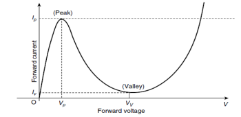
  Electronic symbol of Schottky diode Applications • They are used in fast-switching applications such as in microwave mixers, where the diode should switch conductance states at the rate of the frequency of a microwave local oscillator.• A Schottky diode is used as a square-law detector when bias is zero, whose power output is proportional power to input.• They are used in detectors 5.7 TUNNEL DIODESIn a conventional PN junction diode, the concentration of impurities is in the order of one part in 108. When the impurity concentration is increased to 1 part in 103, the conventional PN diode becomes the tunnel diode. Principle of Operation: In a tunnel diode, the impurity concentration is greatly increased as compared with the PN diode. This reduces the width of the depletion layer to the order of hundred angstroms. According to quantum mechanics, if the barrier is less than 3A0, there is a large probability that particles will tunnel through the potential barrier. This is known as tunneling. The operation can be best explained by considering energy band diagram of P-type and N-type materials. Due to high impurity concentration, there are many holes in valence band of P-type material and many electrons in conduction band of N-type material. Now, if no voltage is applied, the alignment of valence band and conduction band of P-type and N-type is as shown in Figure. Hence, there is no flow of current. Now, if some forward voltage is applied the energy levels of N-region move upward and that of P-region move downward relatively. Therefore, the electrons on the right side of the potential barrier are precisely opposite to the holes on the left side and the corresponding energy band diagram is as shown in Figure. This results in flow of current, whose magnitude gradually increase as forward voltage increase till V = VP which is known as peak voltage.At the peak, as shown in Figure, the voltage energy levels on either side are in perfect alignment. As the voltage is increased beyond VP, the energy levels of the N region move further upward and those of the P region move further downward, causing a condition as shown in Figure. In this condition, some of the N-region electron energy levels are opposite to the band gap and some are opposite to the holes (or empty states). This results in a decrease of current flow, this condition continues till V = VV, called valley voltage. At this voltage, current (I = IV) is minimum. If the voltage is further increased as shown in Figure, then all electrons in the N-region are opposite to the band gap and no currents flows. The corresponding point in the Figure is the VV. If the voltage continues to increase further as shown in Figure, the diode shows characteristics of a normal PN diode. Thus, between peak voltage and valley voltage, the tunnel diode shows negative resistance characteristics. The volt-ampere characteristic curve of a tunnel diode is as shown in Figure.The V-I characteristic of a tunnel diode exhibits the current as multi-valued and the voltage as a single-valued.
 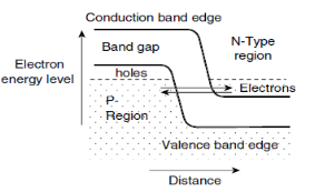 Energy bands in unbiased tunnel diode
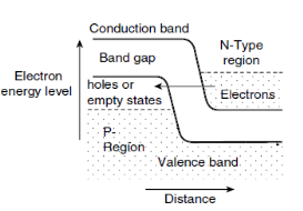 Electron energy levels of N-region are equal to the empty states level on P region.
 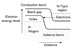 Some N-region electrons energy level are opposite to “band gap,” and some are opposite to holes.
 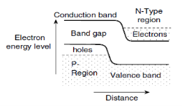 All N-region electrons energy level are opposite to band gap
 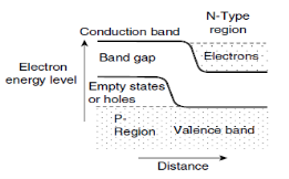 Tunnel diode functions as normal diode
 Symbol of Tunnel diode
V-I characteristics of a tunnel diode Applications• It is used as a high-speed switch. The switching times of the order of nanoseconds are obtained.• As a logic memory storage device• As a microwave oscillator• In a relaxation oscillator• The tunnel diode can be used in bistable, a stable, and monostable circuits. If the operating point is made to vary over the entire range of the voltage, the circuit is in bistable mode. If the operating point is between Vp and Vv, the circuit is a stable. If the operating point is between 0 and Vp, the circuit is monostable.Some important characteristics of a tunnel diode are as follows:• Doping is very high, usually 1000 times of normal diodes.• It has zero breakdown voltage.• It has a dynamic negative resistance region, because when we increase its voltage, the current will decrease beyond the peak voltage.• For an ideal tunnel diode, Vp or Ip should be very large.• It behaves similar to both an amplifier and an oscillator.• In reverse bias, it behaves similar to a good conductor. 5.8 TRANSFERRED ELECTRON DEVICES (TEDS)Transferred Electron Devices (TEDs) are one of the important microwave devices. They are bulk devices that have no junction or gates as compared with microwave transistors, which operate with either junction or gates. Transferred electron devices are fabricated with compound semiconductor materials (e.g) gallium arsenide (GaAs), cadmium telluride (CdTe) and indium phosphide (InP)). They have two energy regions or valleys in the conduction band. The TEDs show a transferred electron effect in which transfer of electrons takes place from lower valley to upper valley in the conduction band. Most of the electrons will be in lower valley at low electric fields. When the electric field strength is increased to higher values, most of the electrons will be transferred into high-energy bands. In the higher-energy bands, the effective mass of electrons is larger than in lower-energy bands. Since the conductivity is directly proportional to mobility, the higher-energy band has lower conductivity than the lower-energy band. Hence, conductivity decreases with an increase in electric field strength. Thus, the current decreases with an increase in voltage, showing negative resistance. Gunn diode is an example of TEDs, and its theory is better explained in the next section.A few differences between microwave transistors and TEDs are as follows:• First, TEDs do not have junctions or gates as in the case of transistors.• TEDs with smaller physical dimensions have a limited power output. In order to get a reasonable power output, the physical dimensions are to be made large as compared with a microwave transistor.• TEDs are made of compound semiconductors from group III–V and II–VI elements (of periodic table) such as gallium arsenide (GaAs), indium phosphide (InP), and cadmium telluride (CdTe); whereas the majority of transistors are made from elements such as germanium or silicon. 5.9 GUNN DIODEIn 1963, Gunn observed a periodic variation of current passing through an N-type GaAs semiconductor.He found the following when a DC bias voltage is applied to the contacts of N-type GaAs or InP:• Current first rises linearly from zero.• Then, it begins to oscillate when a certain threshold is reached.• The time period of oscillation is equal to the travel time of electrons from cathode to anode.This is known as Gunn effect or bulk effect. The device that shows Gunn effect is known as Gunn diode. Gunn diodes are usually fabricated using N-type semiconductor materials (eg. GaAs, and InP); so, they should be associated with electrons rather than with holes. Gunn diode operations do not depend on junction properties. Even though it has no junction, it is called a diode, because it has two terminals (anode and cathode) attached to it. It is an active two-terminal solid-state device and is mainly used as a local oscillator in the microwave frequency range of 1 to 100 GHz. Gunn effect can be explained on the basis of domain formation, two-valley theory of Ridley–Watkins–Hilsum (RWH), or the transfer electron mechanism. Operation and Characteristics of Gunn Diode:The Gunn diode is made up of a single piece of N-doped semiconductor material (e.g. GaAs, InP) with two thinner N+-doped layer contacts on opposite ends. The two N+ layers are required to connect the anode and cathode leads.
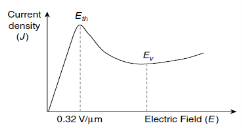 Three-layer structure of Gunn diode J/E curve of a Gunn diode When a DC voltage (V) is applied to the two terminals, an electric field (Eo) will be established across the piece of GaAs (just as in a resistor) (Figure). Figure shows how the current density (J̅ ) through the material varies with the electric field (Eo) across it. We know that the drift velocity (vd), current density, and electric field have the following relations: vd =
 E J= n q
 E Initially, when the electric field is increased, from the above relations it can be seen that the drift velocity and current density increase. Thus, the current density increases with an increase in the electric field, resulting in a positive resistance. This continues till the electric field reaches a value known as threshold value Eth (corresponding threshold voltage Vth). When the electric field is increased beyond the threshold value Eth, the Gunn effect takes place and the current density decreases, causing the device to exhibit negative resistance. This behavior is due to domain formation, which will be explained in the next section. This will continue till the field reaches a value known as Ev (corresponding valley voltage).When the voltage is increased beyond Ev, the current density increases. Thus, the device again exhibits positive resistance. Negative resistance region: In common the current first rises linearly from zero with increasing electric field, however, there is a region between the threshold electric field and valley electric field, where the current decreases as the electric field is increased. This is called the negative resistance region. The dynamic resistance, r, in this voltage range is given by r = dV/dI, r < 0.Basic Modes of OperationDepending on the device characteristics and external circuitry, the Gunn diode can be made to oscillate in any one of the following four frequency modes:• Gunn oscillation mode• Limited space charge accumulation (LSA) mode• Stable amplification mode• Bias circuit oscillation modeThe modes of operations are classified based on the condition:
  vd = electron drift velocityεs = semiconductor dielectric permittivityμn = electron mobilitye = electron chargeno = doping concentrationl = device length Applications of Gunn Diode 1. It is used in Radar transmitters as low power oscillator (e.g. CW Doppler Radar, Police Radar). 2. Gunn diode oscillators with pulsed signal are used in transponders in industry telemetry systems and for air traffic control. 3. It is used in broadband linear amplifier. 4. It is used in sequential logic circuits and fast combinational circuits 5. It is used in microwave receivers as low and medium power oscillator. 6. It is used in parametric amplifier as pump sources. AVALANCHE TRANSIT TIME DEVICESIt is possible to realize a microwave diode that exhibits negative resistance, by providing a delay between voltage and current through the material. In 1958 Read had proposed that there must be a phase delay of more than 90° between RF input voltage and avalanching current if the total voltage go above breakdown voltage in a diode due to the RF input voltage. Such devices are called avalanche transit time devices.At microwave frequencies, avalanche transit time devices produce negative resistance by using carrier impact ionization and transit time in the high voltage region of a semiconductor junction. There are distinct modes of avalanche oscillators, out of which the following three are discussed:1. IMPATT: Impact Ionization Avalanche Transit Time diode2. TRAPATT: Trapped Plasma Avalanche Triggered Transit diode3. BARITT: Barrier injection transit time diode. 5.10 IMPATT DIODEIMPATT diode is abbreviated as impact-ionization avalanche transit time diode. It is an active solid-state device that operates by a reverse bias adequate to cause avalanche breakdown. This is a high-power diode and a very powerful microwave source that is used in high-frequency electronics and microwave devices. They may be operated at frequencies up to about 350 GHz when manufactured with silicon. The IMPATT diode exhibits a dynamic negative resistance that is required for microwave oscillation and amplification applications. This is due to the following two reasons:Impact Ionization avalanche effect: This causes the carrier current to lag behind the ac voltage by 90 degrees.Transit time effect: This causes a further time delay and causes the external current to lag behind the AC voltage by a further 90 degrees.The summation of delay involved in generating avalanche current multiplication along with delay due to transit time through drift space provides the necessary 180° phase difference between the applied voltage and the resulting current in an IMPATT diode.These devices can be classified as follows:• Single drift devices: Devices such as P+NN+, N+PP+, P+NIN+, and N+PIP+ come under this category. Consider the P+NN+ device. In this device, when the P+N junction is reverse biased, it causes an avalanche breakdown. This causes the P+ region to inject electrons into the NN+ region. These electrons move with a saturated velocity. However, the holes injected from the NN+ region do not drift. Hence, these are called single drift devices.• Double drift devices: The example of a double drift device is P+PNN+. In this device, when the PN junction is biased near an avalanche breakdown, electrons drift along the NN+ region and holes drift along the PP+ region. Hence, they are called double drift devices. Principle of Operation of IMPATT Diode :To understand the operation of an IMPATT diode, here we consider the N+PIP+ diode. Let Vb be the reverse bias breakdown voltage that is applied to the IMPATT device. Assume that a sinusoidal waveform V1sinwt is superimposed on Vdc, resulting in a total device voltage V(t) = (Vdc + V1sinwt) as shown in the figure below,
 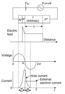 IMPATT diode operation Initially, the device contains a few thermally generated free electrons. When V(t) > Vb breakdown occurs at the N+P junction, these electrons gain energy from the applied voltage and knock off electrons in the valence band to the conduction band. As a result, a new electron hole pair is created. An electron hole pair generated because of such impact ionization is called a secondary electron-hole pair. These secondary electrons again pick up sufficient energy and generate more secondary electron-hole pairs.Therefore, as long as V(t) > Vb, the number of carriers increases exponentially, even beyond the voltage maximum irrespective of magnitude of V(t). This is because of sufficient number of secondary electron hole pairs presence. This exponential increase continues until the sine wave crosses zero and then drops exponentially until the sine wave reaches its negative peak. This avalanche current (generated holes) is injected into the I-region and drifts toward P+ region with saturated velocity along the depletion region.The electrons move toward the positive terminal. In this way, this current will have a one-quarter period (T/4) delay or a 90° phase shift with regard to the applied signal voltage.To achieve the desired 180° phase shift between input voltage and external current, additional T/4 delay is essential. This is made available by the hole drift along the depletion region. It is the property of semiconductor materials that the drift velocity tends to be constant at high field strengths. Since the holes move at the constant velocity vd, the device length may be chosen to provide the necessary delay for a 180° phase shift between the device voltage and current, which is given by,
  Applications • IMPATT diodes are used as microwave oscillators in microwave generators, in modulated output oscillators.• They are used in microwave links, continuous wave radars, and electronic counter measures.• IMPATT diodes are also used as amplification with negative resistance. In police radars, low power transmitters, and intrusion alarm devices are used the high-Q IMPATT diodes. In frequency modulated telecommunication transmitters and continuous wave Doppler radar transmitters are used the low-Q IMPATT diodes. 5.11 TRAPATT DIODEIMPATT and Gunn diodes cannot operate at lower frequencies and they operate at frequencies of 3 GHz or above. In these diodes as it is difficult to increase transit time. A slightly modified structure of the IMPATT diode that can be used at low frequencies is the TRAPATT diode, where TRAPATT stands for trapped plasma avalanche triggered transit mode. In 1967,the first TRAPATT diode was produced, which has an efficiency of 25% and produces 400W at 1000 MHz. Nowadays, efficiencies of 60% to 75% are obtained. Principle of operationThe TRAPATT diode depicted in the figure is a P+NN+ diode that is driven by a large repetitive pulse of current. Breakdown will occur at one of the junctions. Since the current drive is very large, a large collection of disassociated electrons and holes known as plasma is generated.These carriers do not easily recombine. The violent breakdown creates a high electric field shock front that moves across the N-type drift region. After the passage of shock front, the plasma is located in a low field region and is trapped because it takes a long time to clear the drift region of the carriers. When the plasma has been cleared from the drift region, the cycle will be repeated. The formation of plasma in the active region increases the transit time that is required for low-frequency operation. Initially, the device starts oscillating in the IMPATT mode. When the amplitude of oscillations increases, the TRAPATT mode of oscillation is established. The operation can be better explained with help of Figure. When a square current drive is applied to the diode, the output will be as shown in Figure. To better explain the electric field variations, let it be divided into six regions as shown in Figure.
 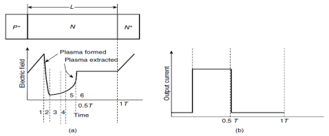 (a) Structure of TRAPATT; (b) Output of TRAPATT Region 1 (Charging): Initially, only thermally generated minority charge carriers are present, and, hence, the current pulse charges up the depletion-layer capacitance. Therefore, the output voltage ramps up as shown in Figure 9.14 (a).Region 2 (Plasma formation): When the electric field becomes more than what is required to cause a breakdown, a large number of carriers is generated. Hence, in region 2, internal current exceeds external current. This results in the formation of a plasma region of a large number of disassociated holes and electrons that are hard to be recombined. As a result of this, conductivity of the medium increases, voltage is reduced to lower values, and the electric field at the depletion region decreases.Region 3 (Plasma extraction): As the voltage drops significantly, the plasma starts being removed. However, the process takes a lot of time. As the plasma gets extracted, the current starts decreasing.As the conductivity is decreasing, the voltage starts building up. In this region, the entire plasma is removed.Region 4 (Residual Plasma extraction): A few charge carriers remain on either side of the depletion layer, resulting in a residual electric field in region 4, which gradually decreases.Region 5 (Charging): In this region, the diode again behaves similar to a capacitor, resulting in the electric pattern.Region 6: The voltage remains constant as the current drops to zero. A sharp rise time current pulse, harmonic rich output of TRAPATT diode is shown in Figure (b).This pulse must be applied to a low-pass filter which is connected to the TRAPATT diode at the input of the waveguide or transmission line. Here the harmonics are not accepted with the filter and thus are reflected back to the TRAPATT diode to activate the next current pulse. Applications• They are used in low-power Doppler radars, microwave beacon landing systems, phased array radars, and so on. Reference Books1. M. Kulkarni, “Microwave and Radar engineering”, 3rd edition, Umesh Publications2. ML Sisodia& GS Raghuvamshi, “Microwave Circuits and Passive Devices”Wiley, 19873. M L Sisodia& G S Raghuvanshi, “Basic Microwave Techniques and LaboratoryManual”, New Age International (P) Limited, Publishers.
 5.1 MICROWAVE BJTSA bipolar junction transistor operated in the microwave region is called a microwave BJT. The operation of the microwave BJT is similar to that of low-frequency transistors. However, the major differences are• GaAs is to be used instead of silicon, because the mobility of electrons is more in GaAs than in Si.• To minimize junction capacitance, the size of the device should be minimized.• The emitter forward resistance is to be minimized by reducing the thickness of the emitter and also by applying maximum possible forward voltage at the emitter junction.• The base transit time is to be reduced by minimizing its thickness and using a graded doping profile.In the analysis and designing of a circuit with microwave BJT, the following points should be considered:A much more complex equivalent circuit model as shown in the figure below is considered. This includes package parasitic capacitance, lead inductance, and resistance.
 Equivalent circuit of microwave BJTCbp —base bond pad capacitanceCep —emitter bond pad capacitanceRbc —base contact resistanceRec —emitter contact resistanceR1, R2, R3 —base distributed resistanceC1, C2, C3 —collector base distributed capacitanceRe —dynamic emitter-base diode resistanceCe —emitter-base diode junction capacitanceRc —collector resistanceLb, Le — base and emitter bond wire inductances Construction: These are usually N-P-N type, because the electron mobility is higher than the hole mobility. The structure of a conventional Si homojunction N-P-N BJT is as shown in the figure below. N-P-N BJT is designed with planar shape as a double diffused epitaxial transistor.
  An N-type epitaxial layer, which acts as a collector, is grown on an N + substrate. An insulating layer of silicon dioxide is grown thermally over the epitaxial layer. The base and emitter layer are formed by diffusion or ion implantation. Proper care is to be taken during the whole process of microwave BJT fabrication so as to reduce package parasites considerably. Contacts are provided by means of openings in the oxide, and connections are made in parallel. The surface geometry of the microwave transistor can be any one of the following:(a) inter-digitized(b) overlay(c) matrixAll the three types are as shown in the figure below. In an inter-digitized geometry, a large number of metallized emitter strips alternating with metallized base strips are present as shown in the figure.This type is used for small signal and power transistors. The second one is the overlay geometry that has a large number of segmented emitters overlying a number of wide metal strips. The third is the matrix or mesh geometry that has an emitter which forms the grid, with the base filling the meshes of this grid with a P+ contact area in the middle of each mesh. Overlay and matrix structures are useful for power transistors.
  Operation of BJT: Microwave BJT behave very similarly to a low-frequency N-P-N bipolar transistor.In an N-P-N BJT, primarily, the collector-base and emitter-base junctions are reverse biased, consequent to the class C condition. The microwave frequency signal is applied between the emitter and base junction, this junction forward bias during the positive portion of the microwave signal. A pulse of current flows through the load connected in the collector circuit. In a proper-designed microwave BJT, the emitter current consists almost all of the electrons and is approximately equal to the collector current, while very small fraction of the emitter current is the base current.The mode mentioned just now is known as an active mode. There are two other operation modes.One is the cut-off mode, in which the emitter and collector junctions are reverse biased and the collector current is negligible, and another mode is the saturation mode, in which both the emitter and collector junctions are forward biased, resulting in a large collector current. Disadvantages: Microwave transistors also suffer from high-frequency limitations. The effects like transit time, inter electrode capacitance etc, come into view again at high frequencies. For example, due to the effect of the inter electrode capacitance high frequency response is limited which causes increase the complexity of the transistor. Lead inductance cause undesirable effect. Ideally, these effects should be kept lowest with appropriate selection of geometry and packaging of BJTs. In addition, they operate at lower frequencies than microwave field effect transistors (FETs). 5.2 MICROWAVE FETSMicrowave FET operates at higher frequencies than those of BJT. Basically, there are two kinds of microwave FETs. They are• Metal Semiconductor FET(MESFET)• Hetero structure FET(HFET)All the above kinds have a source, a drain, and a channel between them. The electric field across the channel can be changed to vary the conductivity of the device. A detailed discussion of MESFETs is given next. 5.3 MESFETConstructional features of a GaAs MESFET are as follows: Initially, a semi-insulating GaAs substrate is taken (To make it semi-insulating, GaAs is doped with chromium). Over that substrate, a thin active layer of N-type GaAs material is grown by ion implantation of donor atoms into the substrate.This active layer has a resistivity that is more than 107 ohm-cm. Three metal contacts for source, gate, and drain are made as shown in the figure. To reduce the contact resistance, the regions beneath the source and drain contacts are diffused with highly doped materials.
  MESFET The channel region is a thin epitaxial N-type GaAs grown on a chromium-doped insulating GaAs substrate. The gate is not a simple P-N junction, but has a Schottky barrier metal contact. The Schottky barrier voltage partially depletes the thin channel under the gate as long as channel doping is in the order of a few 1017cm-3. The positive drain to source voltage will let the current flow through the device.Negative Vgs further reduces the drain to the source current. As VGS approaches the pinch-off voltage, IDS remains constant. The cut-off frequency of the device is given by,
  a = channel heightɛs = semiconductor dielectric permittivityNd = Electron Concentration Applications:• They are used in various applications such as attenuators, mixers, oscillators, amplifiers, phase shifters, transfer switches, frequency multipliers, discriminators, and isolators.• They are used as power amplifiers 5.4 VARACTOR DIODEA varactor is a variable capacitance junction diode. These two terminal devices are also called varicaps or voltacaps. This is a special type of PN junction that is designed to operate in a microwave range. It works on the principle of voltage variable nature of the depletion capacitance. Working: In a PN junction, due to the density gradient, holes diffuse to the N region and electrons diffuse to the P region. This causes a few ions on either side of the junction to be depleted of mobile charges as shown in the figure below. This region is known as the depletion region or space charge region.
  If a forward bias is applied, the carriers move toward the junction as shown in the figure below, which reduces the depletion width.
  If a reverse bias is applied, the carriers move away from the junction; as a result, the depletion width increases as shown in the figure below,
  The variation of width with voltage may be considered a capacitive effect with the depletion region as a dielectric, and P and N regions as parallel plates. This capacitance is known as transition capacitance or junction capacitance and is given by
  Electronic symbol of varactor diode. 5.5 PIN DIODEIt is a variation of the conventional PN junction diode with a small layer between P and N layers. It consists of a layer of intrinsic semiconductors between two heavily doped P- and N-type semiconductors (Figure). The width of the intrinsic region may vary from 10 to 200 micro meters. This long intrinsic region makes the device capable of withstanding high breakdown voltages. The equivalent symbol of the PIN diode is shown in the figure below.
  (a) PIN diode; (b) PIN diode symbol Principle of operation Under the no-bias condition, the I-region of a PIN diode has a very few charge carriers. Holes from the P region and electrons from the N region diffuse into the intrinsic region. The width of the space charge region is inversely proportional to impurity concentration. Therefore, the space charge regions of P and N are very narrow.When a reverse bias is applied, thermally generated electrons move toward the N-region, and thermally generated holes move toward the P-region; as a result of this, a small electron-hole current flows through the device. The space charge region extends into the intrinsic region and almost covers it such that the depletion width (wd) and the width of the intrinsic layer (wI) are equal. The junction capacitance is given by,
  (a) Schottky diode; (b) Forward bias; (c) Reverse bias In the forward-biased condition, the metal is biased positively with regard to the semiconductor. Then, a few electrons from the N-type semiconductor whose thermal energy happens to be many times the average thermal energy will fall down from the potential barrier and move into the metal. Therefore, these electrons are known as hot electrons. Merely those electrons are considered for the forward currents from the semiconductor into the metal. These will have higher energy and velocity till they come into equilibrium with the free electrons of the metal. This raises the temperature of the diode and is, therefore, called a hot carrier diode.An important feature of this diode is that there is no flow of holes from the metal into the semiconductor. Therefore, there is no hole-electron recombination (that takes place in a conventional PN diode). Therefore, if the forward voltage is removed, the time taken by the current to stop is in the order of a few pico seconds, and reverse voltage can be established in this time. As in junction diodes there is no delay effect due to charge storage.
  Electronic symbol of Schottky diode Applications • They are used in fast-switching applications such as in microwave mixers, where the diode should switch conductance states at the rate of the frequency of a microwave local oscillator.• A Schottky diode is used as a square-law detector when bias is zero, whose power output is proportional power to input.• They are used in detectors 5.7 TUNNEL DIODESIn a conventional PN junction diode, the concentration of impurities is in the order of one part in 108. When the impurity concentration is increased to 1 part in 103, the conventional PN diode becomes the tunnel diode. Principle of Operation: In a tunnel diode, the impurity concentration is greatly increased as compared with the PN diode. This reduces the width of the depletion layer to the order of hundred angstroms. According to quantum mechanics, if the barrier is less than 3A0, there is a large probability that particles will tunnel through the potential barrier. This is known as tunneling. The operation can be best explained by considering energy band diagram of P-type and N-type materials. Due to high impurity concentration, there are many holes in valence band of P-type material and many electrons in conduction band of N-type material. Now, if no voltage is applied, the alignment of valence band and conduction band of P-type and N-type is as shown in Figure. Hence, there is no flow of current. Now, if some forward voltage is applied the energy levels of N-region move upward and that of P-region move downward relatively. Therefore, the electrons on the right side of the potential barrier are precisely opposite to the holes on the left side and the corresponding energy band diagram is as shown in Figure. This results in flow of current, whose magnitude gradually increase as forward voltage increase till V = VP which is known as peak voltage.At the peak, as shown in Figure, the voltage energy levels on either side are in perfect alignment. As the voltage is increased beyond VP, the energy levels of the N region move further upward and those of the P region move further downward, causing a condition as shown in Figure. In this condition, some of the N-region electron energy levels are opposite to the band gap and some are opposite to the holes (or empty states). This results in a decrease of current flow, this condition continues till V = VV, called valley voltage. At this voltage, current (I = IV) is minimum. If the voltage is further increased as shown in Figure, then all electrons in the N-region are opposite to the band gap and no currents flows. The corresponding point in the Figure is the VV. If the voltage continues to increase further as shown in Figure, the diode shows characteristics of a normal PN diode. Thus, between peak voltage and valley voltage, the tunnel diode shows negative resistance characteristics. The volt-ampere characteristic curve of a tunnel diode is as shown in Figure.The V-I characteristic of a tunnel diode exhibits the current as multi-valued and the voltage as a single-valued.
  Energy bands in unbiased tunnel diode
 Electron energy levels of N-region are equal to the empty states level on P region.
  Some N-region electrons energy level are opposite to “band gap,” and some are opposite to holes.
  All N-region electrons energy level are opposite to band gap
  Tunnel diode functions as normal diode
 Symbol of Tunnel diode
V-I characteristics of a tunnel diode Applications• It is used as a high-speed switch. The switching times of the order of nanoseconds are obtained.• As a logic memory storage device• As a microwave oscillator• In a relaxation oscillator• The tunnel diode can be used in bistable, a stable, and monostable circuits. If the operating point is made to vary over the entire range of the voltage, the circuit is in bistable mode. If the operating point is between Vp and Vv, the circuit is a stable. If the operating point is between 0 and Vp, the circuit is monostable.Some important characteristics of a tunnel diode are as follows:• Doping is very high, usually 1000 times of normal diodes.• It has zero breakdown voltage.• It has a dynamic negative resistance region, because when we increase its voltage, the current will decrease beyond the peak voltage.• For an ideal tunnel diode, Vp or Ip should be very large.• It behaves similar to both an amplifier and an oscillator.• In reverse bias, it behaves similar to a good conductor. 5.8 TRANSFERRED ELECTRON DEVICES (TEDS)Transferred Electron Devices (TEDs) are one of the important microwave devices. They are bulk devices that have no junction or gates as compared with microwave transistors, which operate with either junction or gates. Transferred electron devices are fabricated with compound semiconductor materials (e.g) gallium arsenide (GaAs), cadmium telluride (CdTe) and indium phosphide (InP)). They have two energy regions or valleys in the conduction band. The TEDs show a transferred electron effect in which transfer of electrons takes place from lower valley to upper valley in the conduction band. Most of the electrons will be in lower valley at low electric fields. When the electric field strength is increased to higher values, most of the electrons will be transferred into high-energy bands. In the higher-energy bands, the effective mass of electrons is larger than in lower-energy bands. Since the conductivity is directly proportional to mobility, the higher-energy band has lower conductivity than the lower-energy band. Hence, conductivity decreases with an increase in electric field strength. Thus, the current decreases with an increase in voltage, showing negative resistance. Gunn diode is an example of TEDs, and its theory is better explained in the next section.A few differences between microwave transistors and TEDs are as follows:• First, TEDs do not have junctions or gates as in the case of transistors.• TEDs with smaller physical dimensions have a limited power output. In order to get a reasonable power output, the physical dimensions are to be made large as compared with a microwave transistor.• TEDs are made of compound semiconductors from group III–V and II–VI elements (of periodic table) such as gallium arsenide (GaAs), indium phosphide (InP), and cadmium telluride (CdTe); whereas the majority of transistors are made from elements such as germanium or silicon. 5.9 GUNN DIODEIn 1963, Gunn observed a periodic variation of current passing through an N-type GaAs semiconductor.He found the following when a DC bias voltage is applied to the contacts of N-type GaAs or InP:• Current first rises linearly from zero.• Then, it begins to oscillate when a certain threshold is reached.• The time period of oscillation is equal to the travel time of electrons from cathode to anode.This is known as Gunn effect or bulk effect. The device that shows Gunn effect is known as Gunn diode. Gunn diodes are usually fabricated using N-type semiconductor materials (eg. GaAs, and InP); so, they should be associated with electrons rather than with holes. Gunn diode operations do not depend on junction properties. Even though it has no junction, it is called a diode, because it has two terminals (anode and cathode) attached to it. It is an active two-terminal solid-state device and is mainly used as a local oscillator in the microwave frequency range of 1 to 100 GHz. Gunn effect can be explained on the basis of domain formation, two-valley theory of Ridley–Watkins–Hilsum (RWH), or the transfer electron mechanism. Operation and Characteristics of Gunn Diode:The Gunn diode is made up of a single piece of N-doped semiconductor material (e.g. GaAs, InP) with two thinner N+-doped layer contacts on opposite ends. The two N+ layers are required to connect the anode and cathode leads.

 Three-layer structure of Gunn diode J/E curve of a Gunn diode When a DC voltage (V) is applied to the two terminals, an electric field (Eo) will be established across the piece of GaAs (just as in a resistor) (Figure). Figure shows how the current density (J̅ ) through the material varies with the electric field (Eo) across it. We know that the drift velocity (vd), current density, and electric field have the following relations: vd =
 IMPATT diode operation Initially, the device contains a few thermally generated free electrons. When V(t) > Vb breakdown occurs at the N+P junction, these electrons gain energy from the applied voltage and knock off electrons in the valence band to the conduction band. As a result, a new electron hole pair is created. An electron hole pair generated because of such impact ionization is called a secondary electron-hole pair. These secondary electrons again pick up sufficient energy and generate more secondary electron-hole pairs.Therefore, as long as V(t) > Vb, the number of carriers increases exponentially, even beyond the voltage maximum irrespective of magnitude of V(t). This is because of sufficient number of secondary electron hole pairs presence. This exponential increase continues until the sine wave crosses zero and then drops exponentially until the sine wave reaches its negative peak. This avalanche current (generated holes) is injected into the I-region and drifts toward P+ region with saturated velocity along the depletion region.The electrons move toward the positive terminal. In this way, this current will have a one-quarter period (T/4) delay or a 90° phase shift with regard to the applied signal voltage.To achieve the desired 180° phase shift between input voltage and external current, additional T/4 delay is essential. This is made available by the hole drift along the depletion region. It is the property of semiconductor materials that the drift velocity tends to be constant at high field strengths. Since the holes move at the constant velocity vd, the device length may be chosen to provide the necessary delay for a 180° phase shift between the device voltage and current, which is given by,
  (a) Structure of TRAPATT; (b) Output of TRAPATT Region 1 (Charging): Initially, only thermally generated minority charge carriers are present, and, hence, the current pulse charges up the depletion-layer capacitance. Therefore, the output voltage ramps up as shown in Figure 9.14 (a).Region 2 (Plasma formation): When the electric field becomes more than what is required to cause a breakdown, a large number of carriers is generated. Hence, in region 2, internal current exceeds external current. This results in the formation of a plasma region of a large number of disassociated holes and electrons that are hard to be recombined. As a result of this, conductivity of the medium increases, voltage is reduced to lower values, and the electric field at the depletion region decreases.Region 3 (Plasma extraction): As the voltage drops significantly, the plasma starts being removed. However, the process takes a lot of time. As the plasma gets extracted, the current starts decreasing.As the conductivity is decreasing, the voltage starts building up. In this region, the entire plasma is removed.Region 4 (Residual Plasma extraction): A few charge carriers remain on either side of the depletion layer, resulting in a residual electric field in region 4, which gradually decreases.Region 5 (Charging): In this region, the diode again behaves similar to a capacitor, resulting in the electric pattern.Region 6: The voltage remains constant as the current drops to zero. A sharp rise time current pulse, harmonic rich output of TRAPATT diode is shown in Figure (b).This pulse must be applied to a low-pass filter which is connected to the TRAPATT diode at the input of the waveguide or transmission line. Here the harmonics are not accepted with the filter and thus are reflected back to the TRAPATT diode to activate the next current pulse. Applications• They are used in low-power Doppler radars, microwave beacon landing systems, phased array radars, and so on. Reference Books1. M. Kulkarni, “Microwave and Radar engineering”, 3rd edition, Umesh Publications2. ML Sisodia& GS Raghuvamshi, “Microwave Circuits and Passive Devices”Wiley, 19873. M L Sisodia& G S Raghuvanshi, “Basic Microwave Techniques and LaboratoryManual”, New Age International (P) Limited, Publishers.
 0 matching results found
Browse by Topics