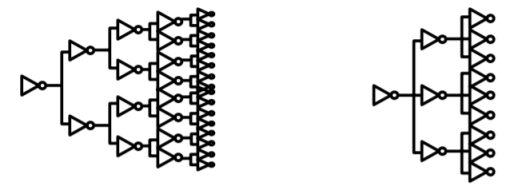
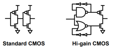
 High gain buffering (skew, jitter, power)– Use push-pull structures vs. standard CMOS Differential signalling (duty cycle, skew, jitter) – Uses more routing resources (i.e., power and area) – Sense amp detects “cross-over” point of differential • P/N ratio duty cycle issues reduced • Full swing signal issues reduced – Possible to design sense amp to provide higher gain stages
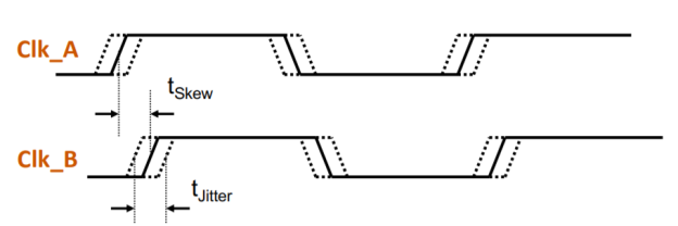
  Low swing signalling (power) – Use lower supply voltage for clock distribution • Could come from explicit power supply or locally generated – Need to transition from full swing PLL to low swing distribution – Need to transition from low swing distribution to full swing flops – Usually done in the higher level portion of distribution • Relatively small portion of overall clock power 3.3 Clock JitterClock jitter is deviation of a clock edge from its ideal location. It plays a key role in the timing budget in a system. It helps the system designers understand the system timing margin.With the increasing system data rates, timing jitter has become critical in system design, as in some instances the system performance limit is determined by the system timing margin.TYPES:Cycle-to-cycle jitter: It measures the change in clock period between any two adjacent clock cycles over 1,000 clock cycles.Period jitter: It measures the maximum deviation of clock period of a clock cycle in the waveform over 10,000 clock cycles.Time interval error jitter: It measures how far each active edge of the clock varies from corresponding edge of an ideal clock.Phase jitter: It is measured by integrating the phase noise across specified frequency offsets from the carrier signal. It is the measurement of the amount of energy present in the specified frequency offsets from the carrier.
 3.4 Supply and Ground Bounce The output voltage of an IC is with respect to the ground of the chip. Hence, in a system, the tiny wire connection between the chip and the lead frame of the package contributes a small amount of inductance in the circuit. When Vout goes low, a spike of current flows through this inductance and creates a voltage spike. A device connected to the output of the circuit indicates a logical zero. This is called as ground bounce. The VDD and ground pins of the package are not at VDD and ground. VDD and ground are established and regulated at the power supply. Therefore, both a resistive component and an inductive component between the package pin and the power supply ground are exists. Therefore, the designer use heavy copper planes that make them as full as possible with as few cuts and holes as possible. But, in fact, this inductance in many high speed circuits is just too large to tolerate. So the bypass capacitors are used in VLSI integrated circuits. The purpose of bypass capacitors is to implement that looks like a regulated VDD and ground right at the package for a short time until the inductance of the planes is overcome. The transient currents when the logic device changes state will not have to flow to and from the power supply, they simply flow to and from the capacitor. 3.5 Power Distribution TechniquesThe need for lower power systems is being optimized for power in addition as performance and space finally varied problems and major challenges relating to low power styles are:-1 Technology Scaling: It relates with the subsequent factors like: Capacitance per node reduces by half-hour, Electrical nodes will increase by 2X, Die size grows by Bastille Day (Moore’s Law), provide Voltage reduces by V-J Day and Frequency will increase by 2X to satisfy these problems comparatively two 7 X active power can increase. 2 Run power: to satisfy frequency demand American state are going to be scaled which ends high run power. a coffee voltage / low threshold technology gate style approach, targeting provide voltage around 1V and operational with reduced thresholds. 3 Dynamic power management techniques, varied provide voltage and swiftness per the activity measure. 4 Low power interconnect, mistreatment advance technology, reduced swing or activity approach. 5 Development of power aware techniques and tools for activity synthesis, logic synthesis and layout optimisation. 6 Power saving techniques: They recycle the signal energies mistreatment the adiabatic change principals rather them dissipating them as a heat and promising in sure applications wherever speed will be trades for low power. 3.6 Power Optimization
 When designing logic networks, one way to reduce power consumption is to capacitance driven by the gate. However, since the gate consumes almost no power when quiescent, the most effective way to reduce its power consumption is to make it change its output as few times possible.
If there is no change in output value the gate is not required. The logic circuit to reduce the number of unnecessary changes to gates output can be designed. To eliminate the glitching the method for power reduction can be used. Glitch reduction may be used in sequential systems.
To stop the propagation of glitches, Sequential machines are incorporated with registers. In sequential timing optimizations is considered as retiming. Figure below shows the flip-flops used to reduce power consumption.
A flip-flop is connected after the logic with high signal transition probabilities. For repeating the timing, extra levels of registers are added. Adding registers are important when there are more glitch-producing segments are present.
However, the number of cycles required to compute the machine outputs should be compatible.
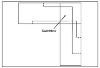
 3.7 Interconnect Routing Techniques Design validation shows the structure and performance of the subsystems. In this the floor plan is checked and the chip after assembly is checked. The block is then extracted, simulated and checked by using timing verifier. By checking the blocks the layout saves size, shape, and pin out of the block. Along with this, wiring errors, chip-level bugs and interface errors emits an active-low signal and the receiving block an active-high signal. The design-rule checking requires CAD tools to build the integrated circuit and to find out the layout errors after tape out of the IC. The layouts designed using the editing systems provide design-rule checking.
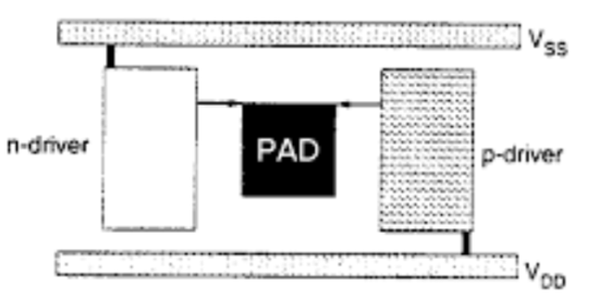
  3.8 Signal Integrity IssuesThe signal integrity problems are related to electromagnetic and are interms of EMI/EMC. In digital system applications, signal is transmitted from one component to other in the form of logic high or low. At the input of receiver, voltage above reference value is taken as logic high, whereas the voltage below the reference value is taken as logic low.Rise Time and Signal Integrity:Due to the significant improvements of the chip fabrication technology, the silicon size is shrinking and the transistor channel length is reduced into sub-micron range. Hence the speed of the logic circuits increases. In deep-sub-micron technology is related with dV/dt or dI/dt, ringing, crosstalk, and power/ground switching noise are existing. Since the systems with faster clock frequency has lower rise time, signal integrity challenges are increasing.Cross Talk Noise:The electromagnetic coupling between the various transmission lines leads to the Crosstalk. Hence, noise picks up on the adjacent signal lines lead to negative logic switching. When the active multiple lines are switching, Crosstalk also involves timing. Depending upon the switching direction, the delays significantly increase/decrease. Because of spacing between the lines, the crosstalk related to signal rise time changes. In order to limit the crosstalk the line space has to be increased and ground guarding band is to be added.Electromigration:Due to high current density, the electrons in the metal moves with high acceleration. And these electrons transfer their momentum to other atoms and the atoms get displaced from their original position and might create voids and hillocks.Hillocks will create shorts and voids will create opens between metal layers. 3.9 I/O Architecture Pad DesignThe circuitry on a chip has to connect with other circuits. These may be chips or display devices, transducers or electro-mechanical devices and the capacitance connected to the chip could be very large. In some cases the devices being driven will require or supply TTL signal levels, in others they may be liable to be short circuits, have high noise levels or be liable to discharge spikes of several kV. Each of these situations will require the imposition of circuitry to interface the chip to the external environment. Most IC designers avoid the problem of pad design and take pad drivers from standard libraries.Physically, pads are the squares of metal, generally 100-150 m m square, that are connected to the pins of the package with bonding wires. The word pad is often used to also include the circuitry that is used to interface the CMOS logic within the IC (typically composed of near minimum-geometry transistors) to the outside world. At least two pads in each circuit will be used to connect the chip to the VDD and VSS power supply lines, while other pads will be used for input connections and output connections. Some pads may also be required to be bi-directional, (for use both with input signals and output signals). In such cases there is usually a control connection to determine the direction of signal transfer.An important function for all pad driver circuitry is the protection of the chip circuitry against destruction due to overvoltage pulses or sustained over voltages. These may be due to electrostatic discharges or due to faults on other circuitry that cause unexpectedly high voltages to be applied to the chip pins.
 Reference Books1. Allen Holberg, “Analog CMOS Design”, Oxford University Press.2. Neil H. E. Weste, David Money Harris, “CMOS VLSI Design: A Circuit & SystemPerspective”, Pearson Publication