UNIT - 4
Digital CMOS Circuits
4.1 MOS Capacitor
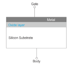
- It is made of a semiconductor body or substrate, an insulator and a metal electrode called a gate.
- The metal comprises of heavily doped n+ poly-silicon layer which behaves as a metal layer.
- The dielectric material used between the capacitor plates is silicon dioxide (SiO2).
- The metal acts as one plate of the capacitor and the semiconductor layer which may be n-type or p-type acts as another plate.
4.2 MOS Transistor Theory
- Flat band voltage is the voltage at which there is no charge on the capacitor plates and hence there is no static electric field across the oxide.
- An applied positive gate voltage larger than the flat band voltage (Vgb > Vfb) then positive charge is induced on the metal semiconductor.
- The negatively charged electrons accumulate at the surface. This is known as surface accumulation.
- If the applied gate voltage is lower than the flat band voltage (Vgb < Vfb) then a negative charge is induced.
- This is only possible by pushing the negatively charged electrons away from the surface exposing the fixed positive charges from donors. This is known as surface depletion.


4.3 C-V Characteristics
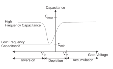
Fig: Capacitance vs. Gate Voltage (CV) diagram
The flatband voltage (Vfb) separates the Accumulation region from the Depletion region. The threshold voltage (Vth) separates the depletion region from the inversion region.
4.4 Non Ideal I-V Effects
The I-V characteristics designed so far neglect many effects that are important in modern deep-submicron processes.
§ Velocity Saturation and Mobility Degradation
§ Channel length modulation
§ Sub threshold conduction
§ Tunneling
§ Junction leakage
§ Body effect
§ Temperature and Geometry dependence
4.5 Technology Scaling
In high performance CMOS circuits certain electrical design rules are taken into consideration.
They are used to develop the mathematical model used in the circuits.
Rules change as the current CMOS fabrication processes are improved and the device dimensions are shrinking.
Hence as the device dimensions are changing the electrical parameters of the devices are also has to be scaled accordingly to apply the previously developed models to the current modern devices and circuits.
Efforts are being taken to make transistors as small as possible to increase speed and circuit complexity per unit of chip area.
In scaling of the MOS devices the basic operational characteristics are preserved by introducing a dimensionless factor.
For this, adjustment in the fabrication process is done and the bias voltage allows proper operation of reduced size devices.
The reduction in lateral dimensions of the MOSFET and interconnects size is known as 'scaling' of the geometric dimensions of the MOSFET.
Advantages:
(1) The integration density improves due to single chip devices.
(2) Enhanced performance in terms of speed and power consumption.
(3) Cost of a chip decreases by twice.
Disadvantages:
1) The power consumption per unit area increases as devices are scaled down. That means scaled devices run increasingly hot. This is a severe performance limitation for scaled devices.
2) The scaling leads to mistakes of having scale proportionally to zero dimension or to zero threshold voltages.
4.6 CMOS Inverters
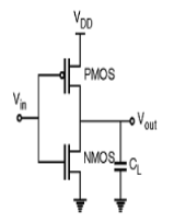
Fig: CMOS inverter
- It consists of PMOS and NMOS FET.
- The input A serves as the gate voltage for both transistors.
- The NMOS transistor has an input from Vss (ground) and PMOS transistor has an input from Vdd. The terminal Y is output.
- When a high voltage (~ Vdd) is given at input terminal (A) of the inverter, the PMOS becomes open circuit and NMOS switched OFF so the output will be pulled down to Vss.
- The truth table of inverter is:
A | Y = A’ |
0 | 1 |
1 | 0 |

Fig. : NOT gate (ref. 1)
4.7 DC Transfer Characteristics
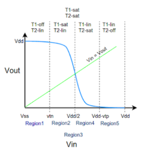
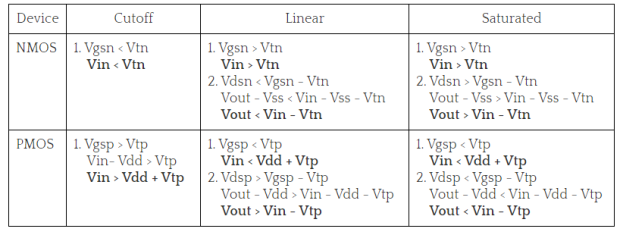
The VTC is divided into five regions (1-5) for easy of understanding. The above shown curve is possible when both T1 and T2 are matched for optimum operation. Optimum operation is achieved when Vin = Vdd/2 we get Vout = Vdd/2 . This can be achieved by adjusting width and length of both T1 and T2 as other parameters like mobility, oxide capacitance vary between different technologies.
Region-1
In this, the input is in the range of (0,Vtn).
- NMOS is in cutoff as Vgs < Vtn
- PMOS is in linear as Vgsp < Vtp and Vdsp > Vgsp -Vtp.
- Zero current flows from supply voltage and the power dissipation is zero.
Region-2
Here, the input is in the range of (Vtn,Vdd/2).
- NMOS is in saturation as Vgs > Vtn and Vout >Vin – Vtn.
- PMOS is in linear region as Vdsp > Vgsp -Vtp.
- Since both the transistors are conducting some amount of current flows from supply in this region.
Region-3
Here the input voltage is Vdd/2. At this point the output voltage is Vdd/2. Here both the NMOS and PMOS are in saturation and the output drops drastically from Vdd to Vdd/2. At this point a large amount of current flows from the supply.
- NMOS is in saturation as Vgs > Vtn and Vout >Vin - Vtn.
- PMOS is in saturation as Vgsp < Vtp and Vdsp < Vgsp -Vtp.
- Large amount of current is drawn from supply and hence large power dissipation.
Region-4
In this region the input voltage is in the range of (Vdd/2 , Vdd-Vtp). Here the PMOS remains in saturation as Vout < Vin - Vtp and Vgsp < Vtp. But the NMOS moves from saturation to linear region since the drain to source voltage now is less than Vgsn-Vtn.
- NMOS is in linear as Vgs > Vtn and Vout < Vin - Vtn.
- PMOS is in saturation as Vgsp < Vtp and Vdsp < Vgsp -Vtp.
- A medium amount of current is drawn as NMOS is in linear region and power dissipation is low.
Region-5
In this region the input voltage is in the range of (Vdd-Vtp,Vdd). Here the PMOS moves from saturation to cutoff as the Vgsp is so high that Vgsp > Vtp. The NMOS still remains in linear as the drain to source voltage now is less than Vgsn-Vtn.
- NMOS is in linear as Vgs > Vtn and Vout < Vin - Vtn.
- PMOS is in cutoff as Vgsp > Vtp.
- Zero current flows from the supply and hence the power dissipation is zero.
4.8 Power Components
High frequencies impose a strict limit on power consumption in computer systems as a whole. Therefore, power consumption of each device on the board should be minimized. Power calculations determine power-supply sizing, current requirements, cooling/heat sink requirements, and criteria for device selection. Power calculations also can determine the maximum reliable operating frequency.
Two components determine the power consumption in a CMOS circuit:
• Static power consumption
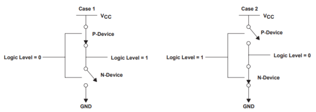
If the input is at logic 0, the n-MOS device is OFF, and the p-MOS device is ON. The output voltage is VCC, or logic 1 and when the input is at logic 1, the associated n-MOS device is biased ON and the p-MOS device is OFF. The output voltage is GND, or logic 0. The source drain diffusion and N-well diffusion form parasitic diodes. The leakage current of the diode is described by the following equation:
Ilkg = Is (eqV/kT – 1 )
Where: Is = reverse saturation current
V = diode voltage
k = Boltzmann’s constant (1.38 × 10⁻²³ J/K)
q = electronic charge (1.602 × 10⁻¹⁹ C)
T = temperature
Static power consumption is the product of the device leakage current and the supply voltage. Total static power consumption, PS, is given by
PS = ∑ (leakage current) * (supply voltage)
Most CMOS data sheets specify an ICC maximum in the 10-µA to 40-µA range, encompassing total leakage current and other circuit features that may require some static current not considered in the simple inverter model. The leakage current ICC (current into a device), along with the supply voltage, causes static power consumption in the CMOS devices. This static power consumption is defined as quiescent, or PS.
PS = VCC * ICC
Where: VCC = supply voltage
ICC = current into a device (sum of leakage currents)
Another source of static current is ∆ICC. This results when the input levels are not driven all the way to the rail, causing the input transistors to not switch off completely.
• Dynamic power consumption
The dynamic power consumption of a CMOS IC is calculated by adding the transient power consumption (PT), and capacitive-load power consumption (PL).
Transient Power Consumption
Transient power consumption can be calculated by
PT = Cpd * VCC2 * f1 * NSW
Where: PT = transient power consumption
VCC = supply voltage
fI = input signal frequency
NSW = number of bits switching
Cpd = dynamic power-dissipation capacitance
Capacitive-Load Power Consumption
Additional power is consumed in charging external load capacitance and is dependent on switching frequency. The following equation can be used to calculate this power if all outputs have the same load and are switching at the same output frequency.
PT = CL * VCC2 * f0 * NSW (CL is the load per output)
Where: PT = capacitive-load power consumption
VCC = supply voltage
fO = output signal frequency
CL = external (load) capacitance
NSW = total number of outputs switching In the case of different loads and different output frequencies at all outputs, equation 6 is used to calculate capacitive-load power consumption.
PT = ∑ (CLn * f0n ) * VCC2
Where: Σ = sum of n different frequencies and loads at n different outputs
fOn = all different output frequencies at each output, numbered 1 through n (Hz)
VCC = supply voltage (V)
CLn = all different load capacitances at each output, numbered 1 through n.
4.9 Power Delay Product
The power-delay product (PDP) is defined as a product of power dissipation and the propagation delay. Figure below shows the shows the PDP input signal waveform.
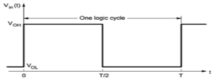
Fig: Ideal square wave
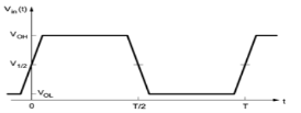
Fig: Finite delay rise and fall time
Hence, PDP = CL·VDD2
4.10 Transmission Gate
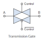
When PMOS and NMOS devices together are connected in parallel then a basic bilateral CMOS switch is created and is known as a “Transmission Gate”. Here, the transmission gate is symmetrical, or bilateral, that is, the input and output are interchangeable. This bilateral operation is shown in the transmission gate symbol below which shows two superimposed triangles pointing in opposite directions to indicate the two signal directions.
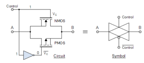
Both MOS transistors are connected back-to-back in parallel with an inverter used between the gate of the NMOS and PMOS to provide the two complementary control voltages. When the input control signal, VC is LOW, both the NMOS and PMOS transistors are cut-off and the switch is open. When VC is high, both devices are biased into conduction and the switch is closed.
When VC = 1, the transmission gate acts as a “closed” switch,
when VC = 0, it operates as a voltage-controlled switch.
The bubble of the symbol indicating the gate of the PMOS FET.
Symbol
Truth Table
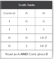 Boolean Expression B = A.Control
4.11 CMOS Combo Logic Design
CMOS Two input NOR Gate
The circuit consists of a parallel-connected n-net and a series-connected complementary p-net. The input voltages VX and VY are applied to the gates of one nMOS and one pMOS transistor.
When either one or both inputs are 1, then p-net is 0 (cut—off).
If both input voltages are 0, then the p-net conducts between the output node and the supply voltage.
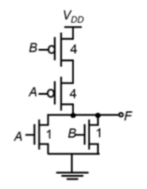
Fig: Layout of CMOS NOR Gate
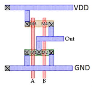
Fig: Stick Diagram of CMOS NOR Gate
CMOS Two-input NAND Gate
Here, the n – net consists of two series connected nMOS transistor conducts between the output node and the ground, if both input voltages are 1. Both of the parallelly connected pMOS transistor in p-net will be off.
For all other input combination, either one or both of the pMOS transistor will be turn ON, while p – net is cut off, thus, conducts between the output node and the power supply voltage.
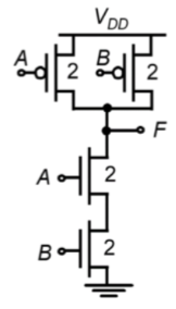
Fig: Layout of CMOS NOR Gate
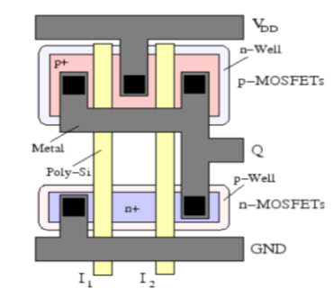
Fig: Stick Diagram of CMOS NOR Gate
4.12 Delays: RC Delay Model
- The RC delay model is a metric used in VLSI design to calculate the signal delay between the input voltage and output voltage of the input signal.
- The input signal is a step function. In this case the transistor can be considered as a switch in series with a resistor.
- A unit nMOS transistor is characterized with resistance or effective resistance, R= Vds/Ids
- Let’s consider a k times transistor unit, here the resistor of the single transistor is R/k, k is the constant here. pMOS transistor has a bigger resistance – 2R .
- nMOS transistors are characterized with higher mobility than pMOS transistors. If the transistor is velocity-saturated, its current and resistance does not depend on the channel length.
- Let’s consider a transistor with gate capacitance C. For a k unit cell, gate capacitance of the transistor is kC.
- Diffusion capacitance depends on the size of drain or source, but with the most common approximation it is also C.
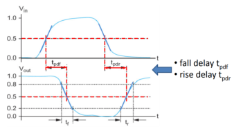
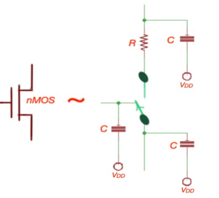
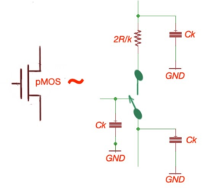
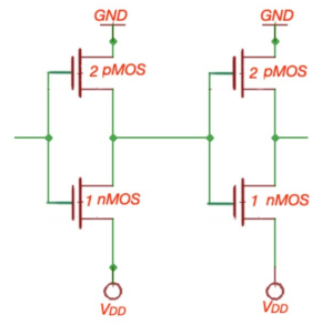
Fig: Equivalent RC circuits
4.13 Linear Delay Model
Normalised delay of a gate can be expressed as the sum of parasitic delay and effort delay . The effort delay depends on the fan-out of the gate, here is a logical effort.
Electrical effort is a situation when a gate is driving identical to itself gates is said to have an electrical effort or fan-out . In case if the load consist of gates different from driving gate, the electrical effort of fan-out can be found by formula, here is the capacitance of the driving gate, and is the capacitance of the load gates that are being driven.
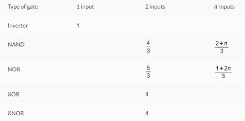
Logical effort of the gate is the ratio of the input capacitance of the gate to the input capacitance of the inverter that delivers the same output current.
4.14 Parasitic Delay
Parasitic delay is the delay when the gate drives zero load. It is comfortable to use the term of normalised parasitic delay, which is the ratio of diffusion capacitance to the gate capacitance of certain process.
Reference Books
1. Allen Holberg, “Analog CMOS Design”, Oxford University Press.
2. Neil H. E. Weste, David Money Harris, “CMOS VLSI Design: A Circuit & System
Perspective”, Pearson Publication