VLSI
UNIT - 5Analog CMOS Design 5.1 Current Sink and SourceCurrent Source:-A current source is a device which when connected to a closed loop of conducting wires or other passive elements (resistor, inductor and capacitor) delivers or absorbs the flow of current through it. A practical voltage source is also a current source.Current Sink:-When a load is connected to a device so that current flows from the power supply through the load and into the device, then the configuration is said to be current sinking. When current flows into the device, it is said to be sinking current. When the term source and sink are used together they figuratively refers to the direction of flow of current in the circuit. 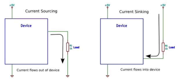 Fig. Current source and sink 5.2 Current MirrorA current mirror is a circuit block which functions to produce a copy of the current flowing into or out of an input terminal by replicating the current in an output terminal. It has a relatively high output resistance which helps to keep the output current constant regardless of load conditions. It has a relatively low input resistance which helps to keep the input current constant regardless of drive conditions.
 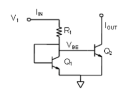 Fig: Current mirror If a current source works as an input, the input section of the current mirror looks like a virtual short circuit and swaps the direction of flow this current to produce a current sink.
 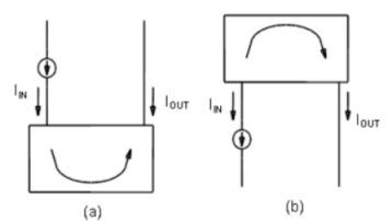 Fig: (a) Sink (b) Source If a current sink is used as an input, the current mirror reflects this current to control current source (figure b); as a result, we obtain a current source. 5.3 Active LoadAn active load or dynamic load is a component or a circuit that functions as a current-stable nonlinear resistor.A high small-signal impedance causing voltage drop would occur if a large resistor is used. Such large AC load impedances may be desirable, for example, to increase the AC gain of some types of amplifier. It is the output part of a current mirror and is represented in an idealized manner as a current source. Usually, it is only a constant-current resistor that is a part of the whole current source including a constant voltage source as well.The load is a resistor, and the current through the resistor is determined by Ohm's law as:Ic = (Vcc – Vout)/Rc.
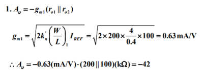
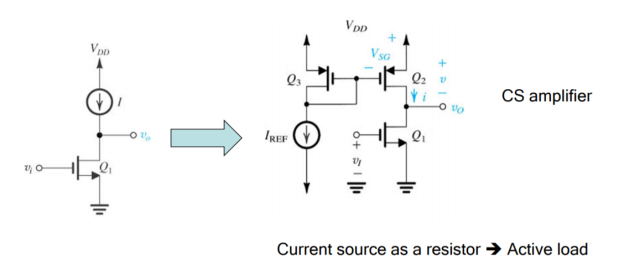 Numerical:1. If VDD=3V, Vtn=|Vtp|=0.6V, kn’=200 A /V2, kp’=65 A/V2, L=0.4 m, W=4 m, ro1=200k , ro2,3 = 100k , IREF=100 A1. What is the small-signal voltage gain, Vo/Vi ? 2. What is the maximum Vo for which the above is valid?
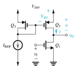 Solution:
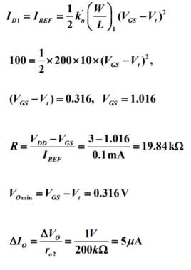
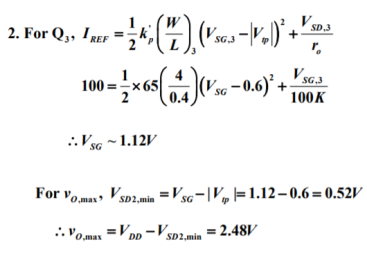 2. If VDD=3V, Q1, Q2 identical L= 1 m, W=100m, Vt=0.7V, kn’=200 A/V2 , ro = 200k1. Determine R for I0=100 A. 2. What is the lowest value for VO ?3. How much IO changes when VO changes 1V?
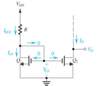 Solution:
 5.4 Current Source and Push-pull InvertersCurrent source inverters
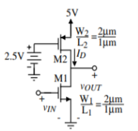
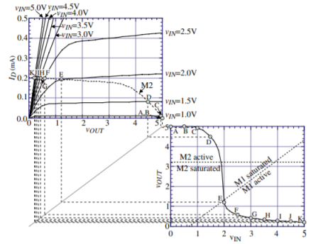
 Large-Signal Voltage Swing Limits of the Current Source Load Inverter Maximum output voltage, vOUT(max): vOUT (max) ≅ VDD Minimum output voltage, vOUT (min): Assume that M1 is nonsaturated. The minimum output voltage is,
 Push Pull Inverter
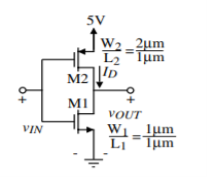
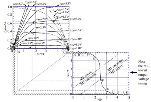
 Small sigal analysis gives the following results:
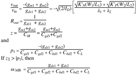 5.5 Common Source AmplifierIn this circuit the MOSFET converts variations in the gate-source voltage into a small signal drain current which passes through a resistive load and generates the amplified voltage across the load resistor.
 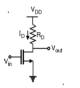 Now from above Figure,
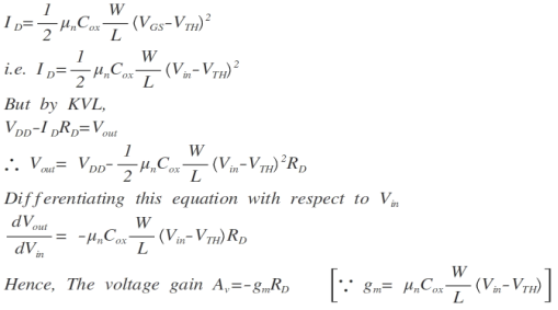 Also, from small signal model of shown in above Figure.By applying KVL,
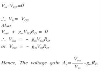 As the gate terminal of MOSFET draws zero current hence it provides a current gain of infinity.Ai = ∞Also Rin = ∞ 5.6 Common Drain AmplifierIt is also known as source follower. In this, drain terminal of the device is common and is directly connected to VDD.In CS amplifier analysis we have seen that in order to achieve the high voltage gain the load impedance should be as high as possible. Therefore for low impedance load the buffer must be placed after the amplifier to drive the load with negligible loss of the signal level. The source follower thus worked as a buffer stage. The source follower is also called as the common drain amplifier.In this circuit, the signal at the gate is sensed and drives the load at the source which allows the source potential to follow the gate voltage. The small signal equivalent circuit of the source follower is:
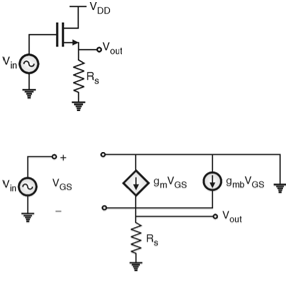
 Form this equation it can be seen that, as gm increases the A v approaches to = 1.Therefore eventually Av approaches to unity.Further, the source follower exhibits high input impedance and a moderate output impedance. The drawback of source follower is nonlinearity due to body effect and poor driving capability of the input signal. 5.7 Common Gate AmplifiersHere the input signal is applied to the source terminal by keeping common gate terminal. This type of amplifier is called as common gate amplifier.Figure below shows the CG amplifier in which the input signal is sensed at the source terminal and the output is produced at the drain terminal. The gate terminal is connected to VB i.e. dc potential which will maintain the proper operating conditions.
 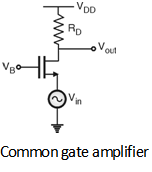 Figure below shows the small signal equivalent circuit of the CG amplifier.
 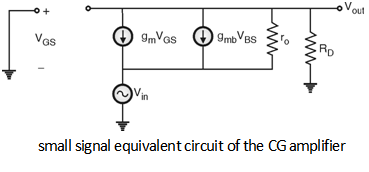 The voltage gain of CG amplifier is given by,Av = = gm RDIn this, the gain is positive and the input impedance is relatively low. Furthermore, the input impedance of common gate stage is relatively low only if the load resistance connected to the drain is small. 5.8 Cascode AmplifierThe cascade of CS stage and CG stage is called as the cascode amplifier. Figure below shows the cascode amplifier circuit in which CS stage and CG stage cascaded.
 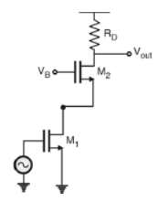 Fig: Cascode amplifierIn this, the output of CS amplifier is connected to the input of CG amplifier. The small signal equivalent circuit of the cascade amplifier is drawn below.
 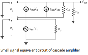 The voltage gain of the cascade amplifier is given by,Av = = gm1Vo1 [(gm2+ g mb2)Vo2+ 1]The small input signal is first amplified by CS stage and the amplified output signal of CS stage is further amplified by the CG stage. It also has the high output impedance. 5.9 Differential Amplifier
The amplifier, which amplifies the difference between two voltages is called Differential Amplifier. It is used to provide high voltage gain and high common mode rejection ratio. It has very low input bias current, very low offset voltage and very high input impedance. It operates in two modes which are differential mode and common mode. Common mode type gives result of zero output while differential mode gives a result of high output, hence this amplifier has high common mode rejection ratio. If two input voltages are equal, then it gives an output voltage of almost zero volts and if the two input voltages are not equal then it gives high output voltage. 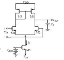 Fig: Differential amplifier
 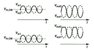 Fig: Differential amplifier waveform 5.10 Operational Amplifier
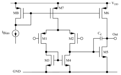 Fig: 2 stage op-amp Open loop differential gainThe gain is obtained by multiplying the gains of the two stages.
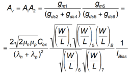 Common mode dc gainApplying the same signal to both inputs the circuit becomes symmetrical and can be studied considering half circuit.
 Offset: The offset is composed of two terms: systematic offset random offset Reference Books1. Allen Holberg, “Analog CMOS Design”, Oxford University Press.2. Neil H. E. Weste, David Money Harris, “CMOS VLSI Design: A Circuit & SystemPerspective”, Pearson Publication
 Fig. Current source and sink 5.2 Current MirrorA current mirror is a circuit block which functions to produce a copy of the current flowing into or out of an input terminal by replicating the current in an output terminal. It has a relatively high output resistance which helps to keep the output current constant regardless of load conditions. It has a relatively low input resistance which helps to keep the input current constant regardless of drive conditions.
  Fig: Current mirror If a current source works as an input, the input section of the current mirror looks like a virtual short circuit and swaps the direction of flow this current to produce a current sink.
  Fig: (a) Sink (b) Source If a current sink is used as an input, the current mirror reflects this current to control current source (figure b); as a result, we obtain a current source. 5.3 Active LoadAn active load or dynamic load is a component or a circuit that functions as a current-stable nonlinear resistor.A high small-signal impedance causing voltage drop would occur if a large resistor is used. Such large AC load impedances may be desirable, for example, to increase the AC gain of some types of amplifier. It is the output part of a current mirror and is represented in an idealized manner as a current source. Usually, it is only a constant-current resistor that is a part of the whole current source including a constant voltage source as well.The load is a resistor, and the current through the resistor is determined by Ohm's law as:Ic = (Vcc – Vout)/Rc.
 Numerical:1. If VDD=3V, Vtn=|Vtp|=0.6V, kn’=200 A /V2, kp’=65 A/V2, L=0.4 m, W=4 m, ro1=200k , ro2,3 = 100k , IREF=100 A1. What is the small-signal voltage gain, Vo/Vi ? 2. What is the maximum Vo for which the above is valid?
 Solution:
 2. If VDD=3V, Q1, Q2 identical L= 1 m, W=100m, Vt=0.7V, kn’=200 A/V2 , ro = 200k1. Determine R for I0=100 A. 2. What is the lowest value for VO ?3. How much IO changes when VO changes 1V?
 Solution:
 5.4 Current Source and Push-pull InvertersCurrent source inverters

 Large-Signal Voltage Swing Limits of the Current Source Load Inverter Maximum output voltage, vOUT(max): vOUT (max) ≅ VDD Minimum output voltage, vOUT (min): Assume that M1 is nonsaturated. The minimum output voltage is,
 Push Pull Inverter

 Small sigal analysis gives the following results:
 5.5 Common Source AmplifierIn this circuit the MOSFET converts variations in the gate-source voltage into a small signal drain current which passes through a resistive load and generates the amplified voltage across the load resistor.
  Now from above Figure,
 Also, from small signal model of shown in above Figure.By applying KVL,
 As the gate terminal of MOSFET draws zero current hence it provides a current gain of infinity.Ai = ∞Also Rin = ∞ 5.6 Common Drain AmplifierIt is also known as source follower. In this, drain terminal of the device is common and is directly connected to VDD.In CS amplifier analysis we have seen that in order to achieve the high voltage gain the load impedance should be as high as possible. Therefore for low impedance load the buffer must be placed after the amplifier to drive the load with negligible loss of the signal level. The source follower thus worked as a buffer stage. The source follower is also called as the common drain amplifier.In this circuit, the signal at the gate is sensed and drives the load at the source which allows the source potential to follow the gate voltage. The small signal equivalent circuit of the source follower is:
 Form this equation it can be seen that, as gm increases the A v approaches to = 1.Therefore eventually Av approaches to unity.Further, the source follower exhibits high input impedance and a moderate output impedance. The drawback of source follower is nonlinearity due to body effect and poor driving capability of the input signal. 5.7 Common Gate AmplifiersHere the input signal is applied to the source terminal by keeping common gate terminal. This type of amplifier is called as common gate amplifier.Figure below shows the CG amplifier in which the input signal is sensed at the source terminal and the output is produced at the drain terminal. The gate terminal is connected to VB i.e. dc potential which will maintain the proper operating conditions.
  Figure below shows the small signal equivalent circuit of the CG amplifier.
  The voltage gain of CG amplifier is given by,Av = = gm RDIn this, the gain is positive and the input impedance is relatively low. Furthermore, the input impedance of common gate stage is relatively low only if the load resistance connected to the drain is small. 5.8 Cascode AmplifierThe cascade of CS stage and CG stage is called as the cascode amplifier. Figure below shows the cascode amplifier circuit in which CS stage and CG stage cascaded.
  Fig: Cascode amplifierIn this, the output of CS amplifier is connected to the input of CG amplifier. The small signal equivalent circuit of the cascade amplifier is drawn below.
  The voltage gain of the cascade amplifier is given by,Av = = gm1Vo1 [(gm2+ g mb2)Vo2+ 1]The small input signal is first amplified by CS stage and the amplified output signal of CS stage is further amplified by the CG stage. It also has the high output impedance. 5.9 Differential Amplifier
 Fig: Differential amplifier
  Fig: Differential amplifier waveform 5.10 Operational Amplifier
 Fig: 2 stage op-amp Open loop differential gainThe gain is obtained by multiplying the gains of the two stages.
 Common mode dc gainApplying the same signal to both inputs the circuit becomes symmetrical and can be studied considering half circuit.
0 matching results found
Browse by Topics