Unit 1
Digital Logic Families
Speed of a logic circuit is determined by the time between the application of input and change in the output of the circuit.
Every gate is connected to a power supply VCC (VDD in the case of CMOS).
A certain amount of current is drawn during its operation. Since each gate can be in a High, Transition or Low state, hence there are three types of currents drawn from power supply:
| |
| |
For TTL, | |
| |
Average Power Dissipation = Vcc * (ICCH + ICCL)/2 | |
| |
For CMOS, | |
| |
Average Power Dissipation = Vcc * ICCT. | |
| |
For TTL logic family, power dissipation does not depends on frequency of operation. For CMOS, the power dissipation depends on the frequency of operation . Power Dissipation: | |
| |
Power dissipation of a circuit defines its battery life: the greater the power dissipation, the shorter the battery life. It is directly proportional to the heat generated by the chip or system hence excessive heat dissipation may increase operating temperature and cause gate circuitry to drift out of its normal operating range. | |
Total power dissipation = static power dissipation + dynamic power dissipation. | |
Figure of merit is a product of propagation delay and power dissipation. It is measured in terms of Pico-Joules (ns ´mW = pJ). Current and voltage parameters define the minimum and maximum limit of current and voltage for input and output of a logic family.
Fig.1: Effects of Fan-in
|
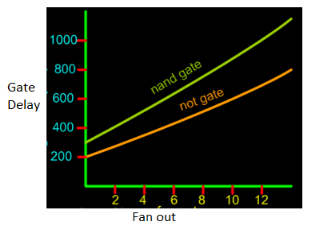
Fig.2: Effects of Fan-out
|
|
They are the voltage levels for logic high and logic low. |
|
|
Gate circuits are made to sustain variations in input and output voltage levels. Variations are usually the result of various factors. |
|
|
|
|
|
|
They are built only with the help of transistors. It has been improved to meet performance requirements. TTL family comprises of: |
|
|
NAND
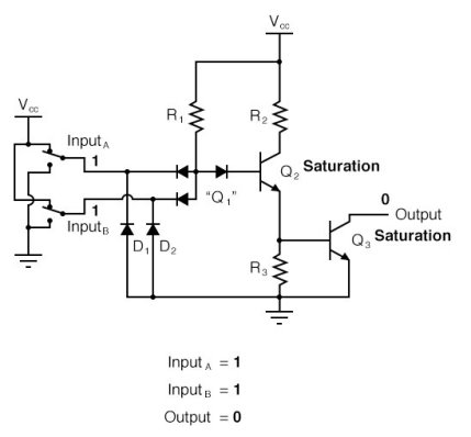
In the single-input (inverter) circuit, grounding the input resulted in an output that assumed the “high” (1) state. In the case of the open-collector output configuration, this “high” state was simply “floating.”
Allowing the input to float (or be connected to Vcc) resulted in the output becoming grounded, which is the “low” or 0 state. Thus, a 1 in resulted in a 0 out, and vice versa.
AND
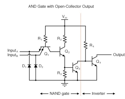
To create an AND function using TTL circuitry, we need to increase the complexity of this circuit by adding an inverter stage to the output, just like we had to add an additional transistor stage to the TTL inverter circuit to turn it into a buffer:
Of course, both NAND and AND gate circuits may be designed with totem-pole output stages rather than open-collector. I am opting to show the open-collector versions for the sake of simplicity.
CMOS inverter
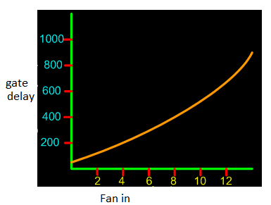
Fig: CMOS inverter
A | Y = A’ |
0 | 1 |
1 | 0 |
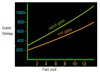
Fig. : NOT gate (ref. 1)
CMOS Two input NOR Gate
The circuit consists of a parallel-connected n-net and a series-connected complementary p-net. The input voltages VX and VY are applied to the gates of one nMOS and one pMOS transistor.
When either one or both inputs are 1, then p-net is 0 (cut—off).
If both input voltages are 0, then the p-net conducts between the output node and the supply voltage.
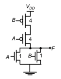
Fig: Layout of CMOS NOR Gate
CMOS Two-input NAND Gate
Here, the n – net consists of two series connected nMOS transistor conducts between the output node and the ground, if both input voltages are 1. Both of the parallelly connected pMOS transistor in p-net will be off.
For all other input combination, either one or both of the pMOS transistor will be turn ON, while p – net is cut off, thus, conducts between the output node and the power supply voltage.
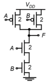
Fig: Layout of CMOS NOR Gate
CMOS driving TTL:
Following figure shows a CMOS gate driving N TTL gates. For such an arrangement to operate properly the following conditions are required to be satisfied,
VOH (CMOS) ≥ VIH(TTL)
VOL (CMOS) ≤ VIL(TTL)
– IOH (CMOS) ≥ NIIH(TTL)
IOL (CMOS) ≥ – NIIL(TTL)
The first possible type of CMOS-to-TTL interface is the one where both ICs are operated from a common supply. We have read in earlier sections that the TTL family has a recommended supply voltage of 5 V, whereas the CMOS family devices can operate over a wide supply voltage range of 3–18 V. In the present case, both ICs would operate from 5 V. As far as the voltage levels in the two logic states are concerned, the two have become compatible. The CMOS output has a VOH(min.) of 4.95V (for VCC =5 V) and a VOL(max.) of 0.05 V, which is compatible with VIH(min.) and VIL(max.) requirements of approximately 2 and 0.8V respectively for TTL family devices. In fact, in a CMOS-to- TTL interface, with the two devices operating on the same VCC, voltage level compatibility is always there. It is the current level compatibility that needs attention. That is, in the LOW state, the output current-sinking capability of the CMOS IC in question must at least equal the input current-sinking requirement of the TTL IC being driven. Similarly, in the HIGH state, the HIGH output current drive capability of the CMOS IC must equal or exceed the HIGH-level input current requirement of TTL IC. For a proper interface, both the above conditions must be met. As a rule of thumb, a CMOS IC belonging to the 4000B family (the most widely used CMOS family) can feed one LS TTL or two low-power TTL unit loads. When a CMOS IC needs to drive a standard TTL or a Schottky TTL device, a CMOS buffer (4049B or 4050B) is used. 4049B and 4050B are hex buffers of inverting and noninverting types respectively, with each buffer capable of driving two standard TTL loads.
Figure below shows a CMOS-to-TTL interface with both devices operating from 5V supply and the CMOS IC driving a low-power TTL or a low-power Schottky TTL device.
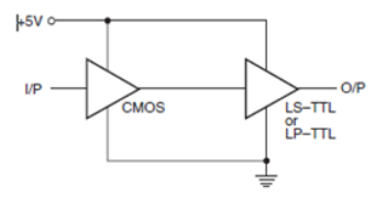
Figure below shows a CMOS-to-TTL interface where the TTL device in use is either a standard TTL or a Schottky TTL.
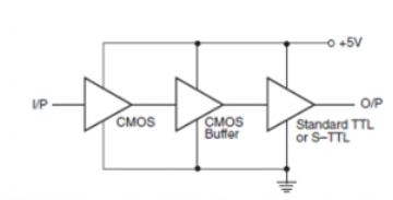
The CMOS-to-TTL interface when the two are operating on different power supply voltages can be achieved in several ways. One such scheme is shown below. In this case, there is both a voltage level as well as a current level compatibility problem.
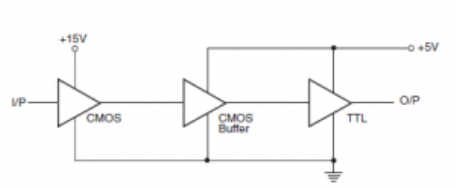
TTL Driving CMOS :
For TTL gate driving N CMOS gates arrangement to operate properly, the following conditions are required to be satisfied:
VOH (TTL) ≥ VIH(CMOS)
VOL (TTL) ≤ VIL(CMOS)
– IOH (TTL) ≥ NIIH(CMOS)
IOL (TTL) ≥ – NIIL(CMOS)
In the TTL-to-CMOS interface, current compatibility is always there. The voltage level compatibility in the two states is a problem. VOH (min.) of TTL devices is too low as regards the VIH (min.) requirement of CMOS devices. When the two devices are operating on the same power supply voltage, that is, 5 V, a pull-up resistor of 10 k_ achieves compatibility as shown in below figure.
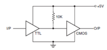
The pull-up resistor causes the TTL output to rise to about 5V when HIGH. When the two are operating on different power supplies, one of the simplest interface techniques is to use a transistor (as a switch) in-between the two, as shown below.
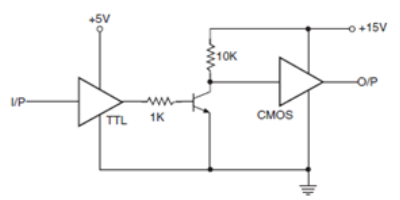
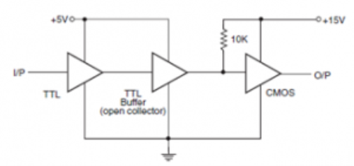
Another technique is to use an open collector type TTL buffer as shown below.
Reference Books:
1. Anand Kumar, “Fundamentals of Digital Circuits”, Prentice Hall of India, 1st Edition.
2. J. F. Wakerly, “Digital Design- Principles and Practices,”, Pearson, 3rd Edition.
3. M. M. Mano, “Digital Design,” Prentice Hall India.


