Unit 4
Sequential Logic Design
1 Bit Memory Cell
Latches are basic storage elements that operate with signal levels (rather than signal transitions). Latches controlled by a clock transition are flip-flops. Latches are edge-sensitive devices. Latches are useful for the design of the asynchronous sequential circuit.
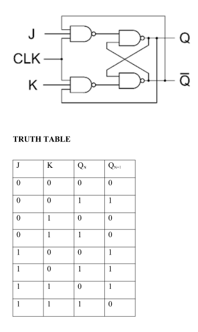
J-K Flip Flop:
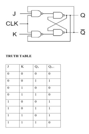
MS J-K flip flop
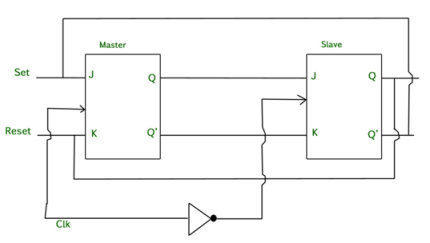
Fig. Master Slave Flip flop
Working of a master slave flip flop –
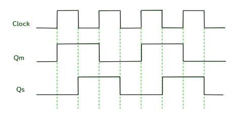
Timing Diagram of a Master flip flop –
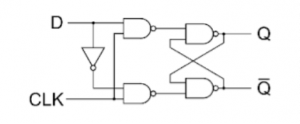
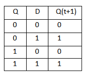
D Flip Flop:
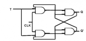
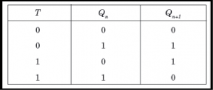
T Flip Flop:
Asynchronous inputs on a flip-flop have control over the outputs (Q and not-Q) regardless of clock input status. These inputs are called the preset (PRE) and clear (CLR). The preset input drives the flip-flop to a set state while the clear input drives it to a reset state.
Hold time is defined as the minimum amount of time after the clock's active edge during which data must be stable. Violation in this case may cause incorrect data to be latched, which is known as a hold violation. Note that setup and hold time is measured with respect to the active clock edge only.
Whenever there are setup and hold time violations in any flip-flop, it enters a state where its output is unpredictable: this state is known as metastable state (quasi stable state); at the end of metastable state, the flip-flop settles down to either '1' or '0'. This whole process is known as metastability. In the figure below Tsu is the setup time and Th is the hold time. Whenever the input signal D does not meet the Tsu and Th of the given D flip-flop, metastability occurs.
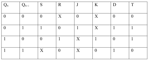
EXCITATION TABLE:
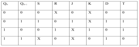
Conversion for flip flops:
i) SR To JK FlipFlop
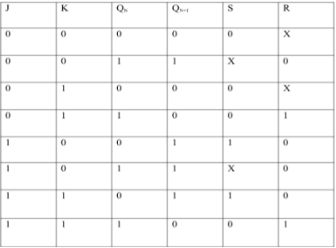
Excitation Functions:
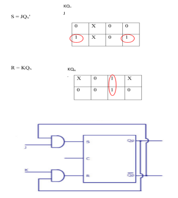
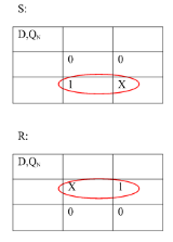
ii) Convert SR To D FlipFlop:
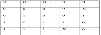
Excitation Functions:
S = D
R = D‘
Registers
Flip-flop is a 1 bit memory cell which can be used for storing the digital data. To increase the storage capacity in terms of number of bits, we have to use a group of flip-flop. Such a group of flip-flop is known as a Register. The n-bit register will consist of n number of flip-flop and it is capable of storing an n-bit word.
Shift registers
The registers which shift the bits towards the right are called “Shift right registers”.
Shift registers are of 4 types and they are:
Serial-In Serial-Out Shift Register (SISO) –
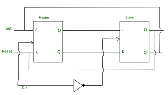
Fig. SISO
Serial-In Parallel-Out shift Register (SIPO) –
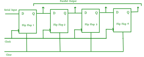
Fig. SIPO
Parallel-In Serial-Out Shift Register (PISO) –
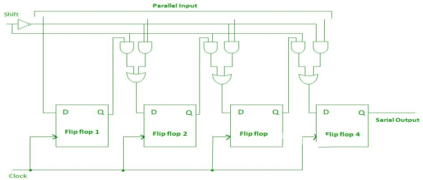
Fig. PISO
Parallel-In Parallel-Out Shift Register (PIPO) –
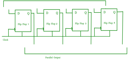
Fig. PIPO
Counters (ring counters, twisted ring counters)
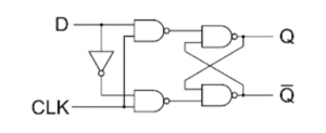

Fig. Ring counter
Ripple counters
In this universal clock is not used and only the first flip flop is driven by main clock and the clock input of rest of the following is driven by output of previous flip flops. 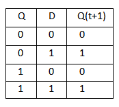
Fig. Asynchronous counter
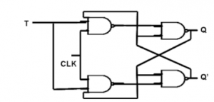
Fig. Timing diagram of Asynchronous counter
Mod-n counters
Truth table is as follows:
Clock pulse | Q3 | Q2 | Q1 | Q0 |
0 | 0 | 0 | 0 | 0 |
1 | 0 | 0 | 0 | 1 |
2 | 0 | 0 | 1 | 0 |
3 | 0 | 0 | 1 | 1 |
4 | 0 | 1 | 0 | 0 |
5 | 0 | 1 | 0 | 1 |
6 | 0 | 1 | 1 | 0 |
7 | 0 | 1 | 1 | 1 |
8 | 1 | 0 | 0 | 0 |
9 | 1 | 0 | 0 | 1 |
10 | 0 | 0 | 0 | 0 |
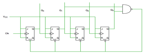
Fig. Decade counter
In the above circuit diagram we used nand gate for Q3 and Q1 and sending this to clear input line as the binary representation of 10 is—
1010
And Q3 and Q1 are 1 here, if we give NAND of these two bits then counter clears at 10 and again starts from the beginning.
Up/down counters
Both Synchronous and Asynchronous counters are capable of counting “Up” or counting “Down”, but their is another more “Universal” type of counter that can count in both directions either Up or Down depending on the state of their input control pin and these are known as Bidirectional Counters.
Bidirectional counters, also known as Up/Down counters, are capable of counting in either direction through any given count sequence and they can be reversed at any point within their count sequence by using an additional control input as shown below.
The circuit above is of a simple 3-bit Up/Down synchronous counter using JK flip-flops configured to operate as toggle or T-type flip-flops giving a maximum count of zero (000) to seven (111) and back to zero again. Then the 3-Bit counter advances upward in sequence (0,1,2,3,4,5,6,7) or downwards in reverse sequence (7,6,5,4,3,2,1,0).
Generally most bidirectional counter chips can be made to change their count direction either up or down at any point within their counting sequence. This is achieved by using an additional input pin which determines the direction of the count, either Up or Down and the timing diagram gives an example of the counters operation as this Up/Down input changes state.
Nowadays, both up and down counters are incorporated into single IC that is fully programmable to count in both an “Up” and a “Down” direction from any preset value producing a complete Bidirectional Counter chip. Common chips available are the 74HC190 4-bit BCD decade Up/Down counter, the 74F569 is a fully synchronous Up/Down binary counter and the CMOS 4029 4-bit Synchronous Up/Down counter.
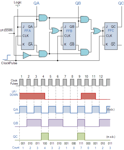
Synchronous Counter
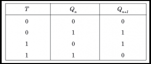
Fig. synchronous counter
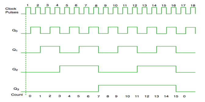
Fig. The timing diagram of the synchronous counter
Lockout
Sometimes a counter may find itself in some unused states, this happen when if next state of some unused state is again some unused one and if by chance the counter happens to find itself in some unused state and never arrives at in used state then this condition is called “Lock Out”.
Solution:
An additional circuit is require to ensure that “lock out” does not occur. The counter should be designed using the next state to be initial state from the unused state.
To avoid lock out condition the unused states are introduced in front of used states from the above state diagram the 1,4,5,6 and 7 is the sequence and unused states are 0,3 and 6 the states are introduced in front of us States 1,4,5 and 7 respectively.
Clock Skew
Clock skew (sometimes called timing skew) is a phenomenon in synchronous digital circuit systems (such as computer systems) in which the same sourced clock signal arrives at different components at different times. The instantaneous difference between the readings of any two clocks is called their skew.
Clock jitter.
Clock jitter is deviation of a clock edge from its ideal location. Understanding clock jitter is very important in applications as it plays a key role in the timing budget in a system. With the increasing system data rates, timing jitter has become critical in system design, as in some instances the system performance limit is determined by the system timing margin. So a good understanding of the timing jitter becomes very important in system design.
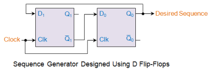
The sequence generators are nothing but a set of digital circuits which are designed to result in a specific bit sequence at their output. There are several ways in which these circuits can be designed including those which are based on multiplexers and flip-flops. Here in this article we deal with the designing of sequence generator using D flip-flops.
As an example, let us consider that we intend to design a circuit which moves through the states 0-1-3-2 before repeating the same pattern. The steps involved during this process are as follows.
For example, look at the orange shaded row in Table I in which the present and the next states 1 and 0 (respectively) result in D1 to be 0. The same row also shows the case wherein
Present States | Next States | Inputs of D flip-flops | |||
Q1 | Q0 | Q1+ | Q0+ | D1 | D0 |
0 | 0 | 0 | 1 | 0 | 1 |
0 | 1 | 1 | 1 | 1 | 1 |
1 | 1 | 1 | 0 | 1 | 0 |
1 | 0 | 0 | 0 | 0 | 0 |
Now its time to derive the Boolean expressions for D1 and D0. This can be done using any kind of simplification technique including K-map. However as our example is quite simple, we can just use the Boolean laws to solve for D1 and D0. Thus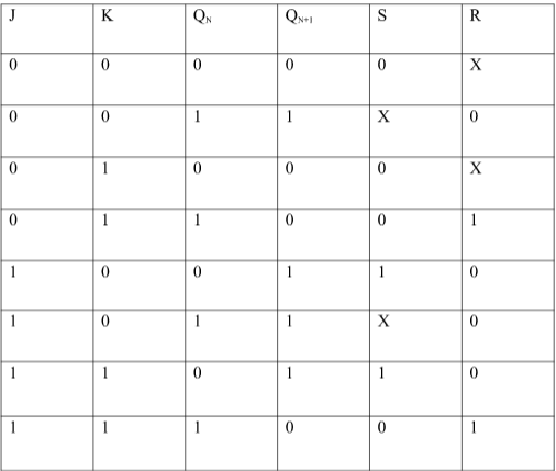
Having known the inputs to either of the D flip-flops, now we can design our sequence generator as shown in this figure.
Reference Books:
1. Anand Kumar, “Fundamentals of Digital Circuits”, Prentice Hall of India, 1st Edition.
2. J. F. Wakerly, “Digital Design- Principles and Practices,”, Pearson, 3rd Edition.
3. M. M. Mano, “Digital Design,” Prentice Hall India.
