Unit – 6
Programmable Logic Devices
A logic device is an electronic component which performs a definite function which is decided at the time of manufacture and will never change. For example, a not gate always inverts the logic level of the input signal and does/can-do-nothing else.
On the other hand, Programmable Logic Devices (PLDs) are the components which do not have a specific function associated with them. These can be configured to perform a certain function by the user, on a need basis and can further be changed to perform some other function at the later point of time, i.e. these are re-configurable. However, the amount of flexibility offered depends on their type. The classification of Programmable Logic Devices is as follows:
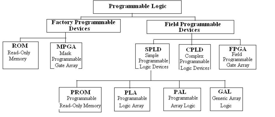
A programmable read-only (PROM) memory is a device which permanently stores binary information. It differs from a normal ROM because it can be programmed electrically once using a PROM programmer. This programmable logic device has Fixed AND arrays and Programmable OR arrays. The block diagram of a PROM is shown below:

It consists of n input lines and m output lines. Each bit combination of the input variables is called an address. Each bit combination that comes out of the output line is called a word. The number of bits per word is equal to the number of output lines, m. The address specified in binary number denotes one of the minterms of n variables. The number of distinct addresses possible with n-input variables is 2n. An output word can be selected by a unique address, and since there are 2n distinct addresses in a PROM, there are 2n distinct words in the PROM. The word available on the output lines at any given time depends on the address value applied to the input lines.
Consider a 64x4 PROM. The PROM consists of 64 words of 4 bits each. This means that there are 4 output lines and particular word from 64 words presently available on the output lines is determined from the six input lines. There are only 6 inputs in a 64X4 PROM because 26 =64, and with six variables we can specify 64 addresses or minterms. For each address input, there is a unique selected word. Thus if the input address is 00000, word number 0 is selected and applied to the output lines. The following figure shows the internal logic construction of a 64X4 PROM.
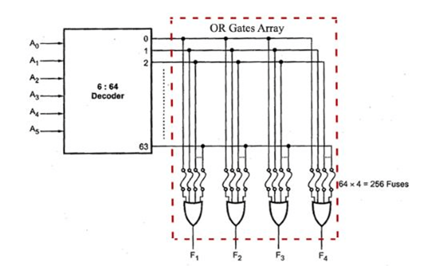
The six input variables are decoded in 64 lines by means of 64 AND Gates and 6 inverters. Each output of the decoder represents one of the minterms of the six variables. The 64 outputs of the decoder are connected through fuses to each OR Gate. Only 4 fuses are shown in the diagram, but actually each OR gate has 64 inputs and each input goes through a fuse that can be blown as desired.
Thus each output provides the sum of all the minterms on n-input variables. We also know that any Boolean function can be expressed in sum of minterms form. By breaking the links of those minterms not included in the function, each PROM output can be made to represent the Boolean function of one of the output variables in the combinational circuit. For an n-input, m-output combinational circuit, we need a 2n x m PROM.
The combinational circuit do not use all the minterms every time. Occasionally they have don’t care conditions. Don’t care condition when implemented with a PROM becomes an address input that will never occur. The result is that not all the bit patterns available in the PROM are used, which may be considered a waste of available equipment.
For cases where the number of don’t care conditions is excessive, it is more economical to use Programmable Logic Array (PLA). The concept is similar to PROM, however it does not generate all the minterms as in the case of PROM. It has both sections of the AND and OR Arrays as programmable, i.e. there is a Programmable AND Array and Programmable OR Array as well. (both AND and OR gates have fuses at the inputs).
The following figure shows the block diagram of PLA:

It consists of n-inputs, m outputs, k-product terms and m sum terms. The product terms constitute a group of k AND gates and the sum terms constitute a group of m OR gates. Fuses are inserted between all n inputs and their complement values to each of the AND gates. Fuses are also provide between the outputs of the AND gates and the inputs of the OR Gates. The third set of fuses in the output inverters allows the output function to be generated either in the AND-OR form or in the AOI form.
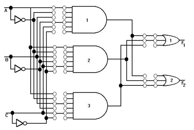
The following figure shows the internal construction of PLA having 3-inputs, 3 product terms and two outputs. The size of the PLA is specified by the number of inputs, the number of product terms and the number of outputs.
Programmable array logic (PAL) is a programmable logic device with a fixed OR array and a programmable AND array. Because only AND gates are programmable, PAL is easier to program, but is not as flexible as the PLA. Figure below shows the array logic of typical PAL.
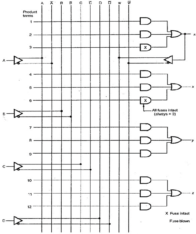
It has 4 inputs and 4 outputs. Each input has buffer and inverter gate. Please note that two gates are shown with one composite graphic symbol with normal and complement outputs. Each section in the figure has three programmable AND gates and one fixed OR gate. The output of section 1 is connected to a buffer-inverter gate and then feedback into the inputs of the AND gates, through fuses. This allows the logic designer to feed an output function back as an input variable to create a new function.
FPGAs are based on gate array technology unlike the PROM technology of early PLDs. These devices comprise of configurable logic blocks (CLBs) along with an interconnection matrix running in-between. FPGAs work based upon the look-up tables (LUTs) and the flip-flops which form a part of CLB. The user has to program the CLBs to perform a certain logical function and then use the interconnection matrix to connect one or more logic blocks together. Further, they comprise of input-output (I/O) ports facilitating the design both from the point of programming as well as debugging.
These devices are capable of implementing state-machine based sequential designs along with the designs based on combinational logic. FPGAs are used to realize more complex designs when compared to CPLDs due to their high density. Moreover, FPGAs offer the customer the flexibility to design/re-design the logic even after being deployed in the work field which gives them the name field-programmable.
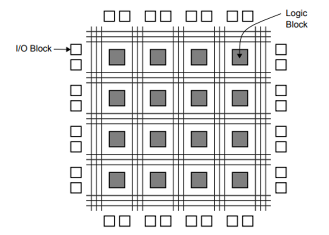
Fig: Architecture of FPGA
CPLDs are denser than PALs and comprise of a large number of programmable logical elements. The interconnection between these macro cells is to be established by the user through the interconnecting network. Here sum-of-product establishing logical elements are combined together to form structures in order to reduce the number of input-output (IO) pins. This facilitates the implementation of more complex logic design with slightly worse propagation time when compared to that of PALs. These offer predictable timing characteristics making them most suitable for critical control applications with high performance. CPLDs are preferred to implement combinational logic based designs.
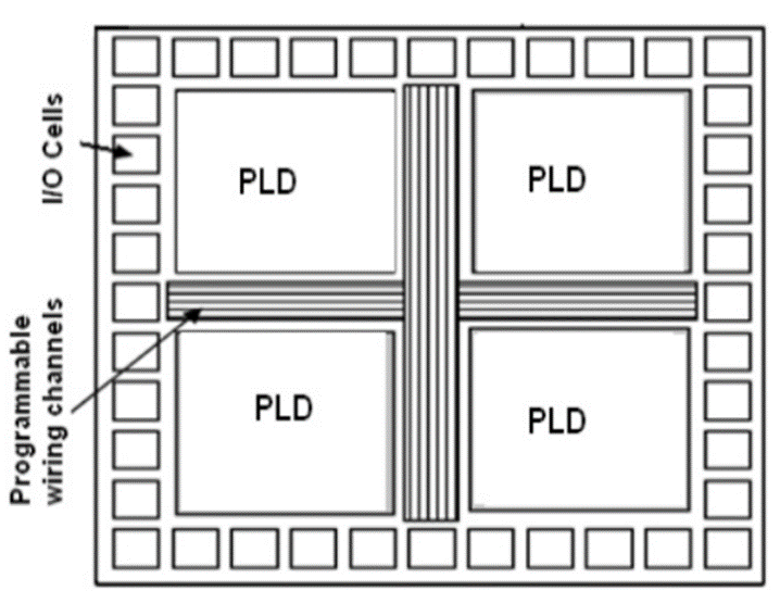
Fig: Architecture of CPLD
The building block of the CPLD is the macro cell, which contains logic implementing disjunctive normal form expressions and more specialized logic operations.
The programmable interconnect in the centre allows connection to the logic block macro cells and the I/O cell arrays.
MEMORY ORGANIZATION AND OPERATION
All memory, regardless of its type or use, consists of locations for storing binary information or bits. Each location is identified by an address. A word is the fundamental group of bits used to represent one entity of information such as one numerical value. The word size- the number of bits in a word- varies among computer systems and may range from 4 to 64 or more bits. The word size is usually expressed as a certain number of bytes.
A memory location is thus a set of devices capable of storing one word. Eg: each memory location in a 8-bit microcomputer might consist of eight latches that store one bit each. The capacity or size of a memory is the total number of bits or bytes or words that it can store. For example, a memory size of 211 =2048 is said to be 2K.
Every memory system requires several different types of input and output lines to perform the following functions:
1) Select the address in memory that is to be accessed for a read or write operation.
2) Select either a read or a write operation to be performed.
3) Supply the input data to be stored in memory during a write operation.
4) Hole the output data coming from memory during a read operation.
5) Enable/ disable the memory, so that it will/ will not respond to the address inputs and read/ write command.
The following figure illustrates these basic functions in a simplified diagram of a 32x4 memory that stores 32, 4-bit words.
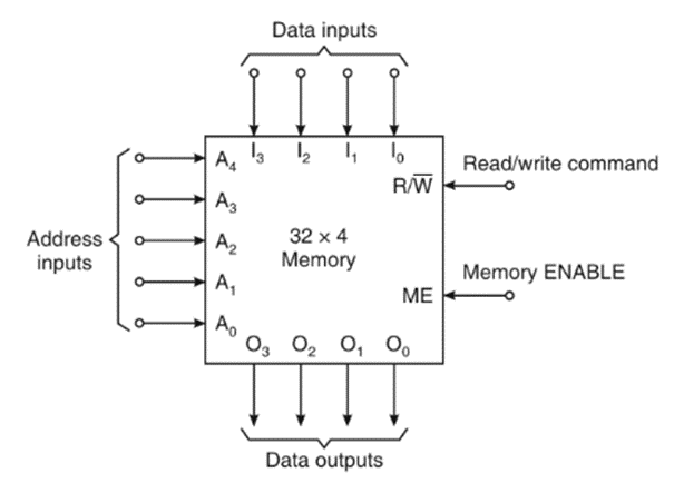
Since the word size is 4-bit, there are 4 data input lines and 4 data output lines. During a write operation, the data to be stored in memory have to be applied to the data input lines. During a read operation, the word being read from memory appears at the data output lines.
Address Inputs
Since this memory stores 32 word, it has 32 different storage locations and therefore 32 different binary addresses ranging from 00000 to 11111. Thus there are 5 address inputs A0 to A5. To access one of the memory locations fro a read or write operation, the 5-bit address code for that particular location is applied to the address inputs.
The R/ input
input
The Read/write (R/ input line determines the memory operation that would take place. Some memory systems use two separate inputs, one for read and one for write. When a single (R/
 input is used, the read operation takes place for (R/
 =1 and the write operation takes place for (R/
 =0.
=0.
Memory ENABLE
Many memory systems have some means of completely disabling all or part of the memory so that it does not respond to the other inputs. A LOW on this input disables the memory, preventing it to respond to address and (R/ inputs.
EXPANDING MEMORY SIZE
Memory chips can be combined together to produce a memory, with desired number of locations. To obtain a memory of capacity m words, using the memory chips with M words each, the number of chips required is an integer next higher to the value m/M. These chips are to be connected in the following way:
1) Connect the corresponding address lines of each chip individually.
2) Connect the RD input of each chip together. Similarly, connect the WR inputs.
3) Use a decoder of proper size and connect each of its outputs to one of the CS terminals of memory chips. Eg: if eight chips are to be connected, a 3-line to 8-line decoder is required to select one out of the eight chips at any one time.
Consider the following example:
Obtain a 2048 x 8 memory using 256 x 8 memory chips.
Solution:
The number of chips required is 2048/256 = 8. At any one time, only one of the 2048 locations is to be accessed, which will be in one of the eight chips. This means only one of the eight chips must get selected at a time.
For selecting one out of 2048 locations, the number of address lines required is 11 (211 = 2048). The lower order address lines A7- A0 will be same for each chip, and the higher order 3 bits of the address A10- A8 must select one out of the eight chips. For this purpose, a 3-line to 8 –line decoder is used. The memory connections are shown below:
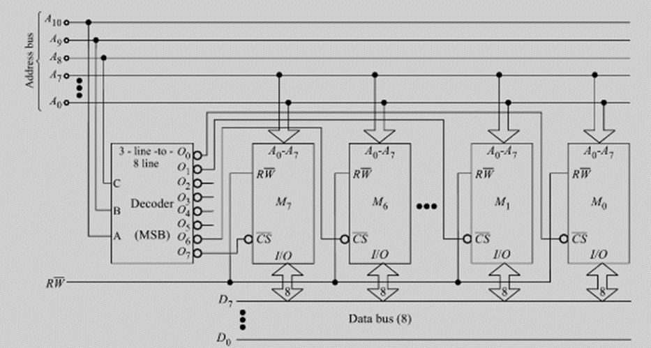
We have assumed a common terminal (R/ for read and write. For the read operation, logic 1 is to be applied to (R/
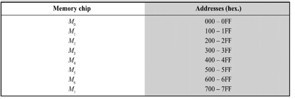
 , whereas logic 0 is to be applied for write operation. The chip select input is assumed to be active low. The addresses of the chips are given below:
CLASSIFICATION OF MEMORIES
To meet the growing needs for semiconductor memory, there are many types and technologies that are used. As the demand grows new memory technologies are being introduced and the existing types and technologies are being further developed.
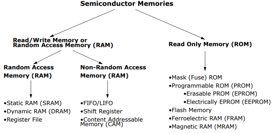
There are two main types or categories that can be used for semiconductor technology. These memory types or categories differentiate the memory to the way in which it operates:
RAM - Random Access Memory: As the names suggest, the RAM or random access memory is a form of semiconductor memory technology that is used for reading and writing data in any order - in other words as it is required by the processor. It is used for such applications as the computer or processor memory where variables and other stored and are required on a random basis. Data is stored and read many times to and from this type of memory.
Random access memory is used in huge quantities in computer applications as current day computing and processing technology requires large amounts of memory to enable them to handle the memory hungry applications used today. Many types of RAM including SDRAM with its DDR3, DDR4, and soon DDR5 variants are used in huge quantities.
ROM - Read Only Memory: A ROM is a form of semiconductor memory technology used where the data is written once and then not changed. In view of this it is used where data needs to be stored permanently, even when the power is removed - many memory technologies lose the data once the power is removed.
As a result, this type of semiconductor memory technology is widely used for storing programs and data that must survive when a computer or processor is powered down. For example the BIOS of a computer will be stored in ROM. As the name implies, data cannot be easily written to ROM. Depending on the technology used in the ROM, writing the data into the ROM initially may require special hardware. Although it is often possible to change the data, this gain requires special hardware to erase the data ready for new data to be written in.
Each of the semiconductor memory technologies outlined below falls into one of these two types of category. Each technology offers its own advantages and is used in a particular way, or for a particular application.
1) EPROM
This is an Erasable Programmable Read Only Memory. These semiconductor devices can be programmed and then erased at a later time. This is normally achieved by exposing the semiconductor device itself to ultraviolet light. To enable this to happen there is a circular window in the package of the EPROM to enable the light to reach the silicon of the device. When the PROM is in use, this window is normally covered by a label, especially when the data may need to be preserved.
The PROM stores its data as a charge on a capacitor. There is a charge storage capacitor for each cell and this can be read repeatedly as required. However it is found that after many years the charge may leak away and the data may be lost. Nevertheless, this type of semiconductor memory used to be widely used in applications where a form of ROM was required, but where the data needed to be changed periodically, as in a development environment, or where quantities were low.
2) EEPROM
This is an Electrically Erasable Programmable Read Only Memory. Data can be written to these semiconductor devices and it can be erased using an electrical voltage. This is typically applied to an erase pin on the chip. Like other types of PROM, EEPROM retains the contents of the memory even when the power is turned off. Also like other types of ROM, EEPROM is not as fast as RAM.
3) DRAM
Dynamic RAM is a form of random access memory. DRAM uses a capacitor to store each bit of data, and the level of charge on each capacitor determines whether that bit is a logical 1 or 0.
However these capacitors do not hold their charge indefinitely, and therefore the data needs to be refreshed periodically. As a result of this dynamic refreshing it gains its name of being a dynamic RAM. DRAM is the form of semiconductor memory that is often used in equipment including personal computers and workstations where it forms the main RAM for the computer. The semiconductor devices are normally available as integrated circuits for use in PCB assembly in the form of surface mount devices or less frequently now as leaded components.
4) SRAM
This form of semiconductor memory gains its name from the fact that, unlike DRAM, the data does not need to be refreshed dynamically.
These semiconductor devices are able to support faster read and write times than DRAM (typically 10 ns against 60 ns for DRAM), and in addition its cycle time is much shorter because it does not need to pause between accesses. However they consume more power, they are less dense and more expensive than DRAM. As a result of this SRAM is normally used for caches, while DRAM is used as the main semiconductor memory technology.
5) NVRAM
NVRAM is random-access memory that retains its information when power is turned off (non-volatile). This is in contrast to dynamic, random-access memory (DRAM) and static random-access memory (SRAM), which both maintain data only for as long as power is applied. The best-known form of NVRAM memory today is flash memory.
In this section we will discuss how to implement a combinational circuit using the PLD’s discussed above.
Example: Design a BCD-to-Excess3 code converter using
(a) PROM (b) PLA (c) PAL
Solution:
The BCD to Excess-3 code converters truth table is given below:
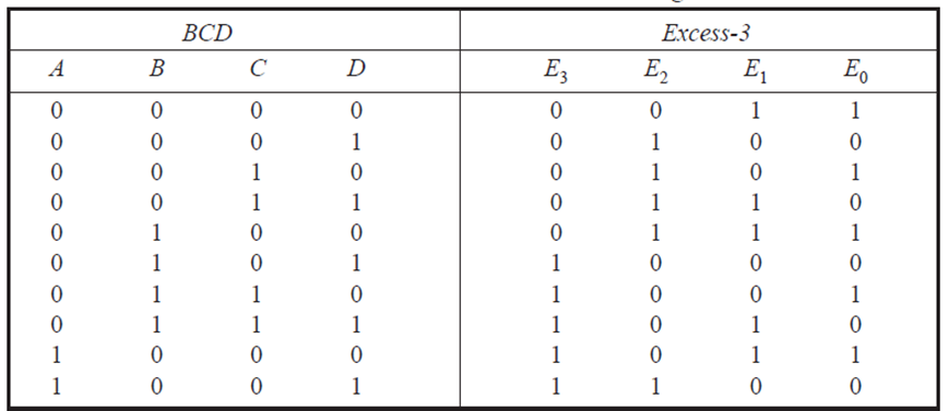
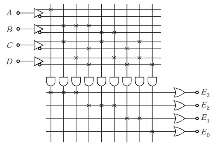
(a) For the design using PROM, a PROM size of 10x4 is required, but since PROM of this size does not exist, therefore a PROM size of 16x4 is to be used. Data is to be stored in the PROM at the addresses corresponding to the BCD code, the data is the Excess-3 code. For example, at the address 000, the data stored is 0011 and at the address 1001 the data stored is 1100.
(b) Logical expressions can be written for E3, E2, E1, E0 outputs in terms of A, B, C, D inputs. To reduce the hardware requirements, these expressions can be minimized using K-Maps.
The simplified expressions are:
E3= A+BC+BD
E2= BC’D’+B’C+B’D
E1=C’D’+CD
E0=D’
The size of the PLA required is:
No. Of inputs = 4
No. Of Outputs = 4
No. Of product terms = 9
Thus the circuit can be realized as follows:
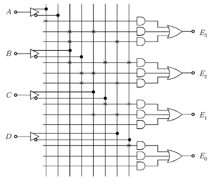
(c) The required size of PAL is
No. Of inputs = 4
No. Of outputs = 4
Minimum number of AND Gates for each output = 3
Thus the circuit can be realized as follows:
