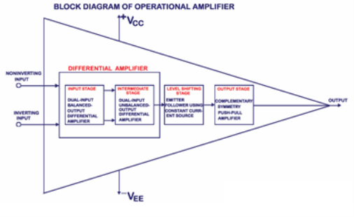
Block Diagram of Operational Amplifier (Op-Amp)
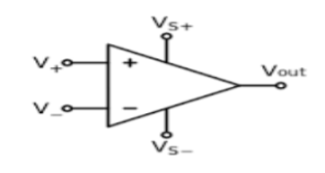
Vo = A [ Vin(+) – Vin(-)] where A is the gain of the amplifier.
The circuit shown below is a dual-inputbalanced-output differential amplifier.Here in this circuit,the two input signals (dual input), vin1 and vin2, are applied to the bases B1 and B2 of transistors Q1 and Q2.
The output vo is measured between the two collectors C1 and C2 which are at the same dc potential.Because of the equal dc potential at the two collectors with respect to ground,the output is referred as a balanced output.
1) Set the dc voltages +VCC and –VEE at 0
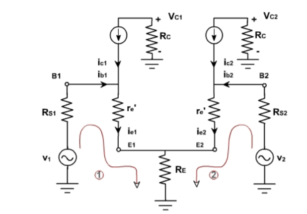
2) Substitute the small signal T equivalent models for the transistors Figure below shows resulting ac equivalent circuit of the dual input balanced output differential amplifier
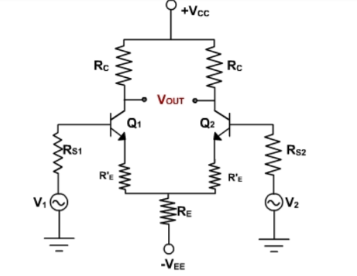
Form the circuit
Writing the Kirchhoff’s voltage equations for loops (1) and (2) is given by
vin1 -Rin1 ib1 – re ie1 – RE(ie1 + ie2) =0
vin2 – Rin2ie2 – reie2 – RE (ie1+ie2) =0
Substituting current relations ib1 = ie1/ Bac and ib2 = ic2/ Bac yields
vin1 -Rin1. ie1/ Bac– re ie1 – RE(ie1 + ie2) =0
vin2 – Rin2ie2/Bac – reie2 – RE (ie1+ie2) =0
Generally, Rin1/Bac and Rin2/Bac values are very small therefore we shall neglect them hence
( re + RE ) ie1 + RE2 ie2 = v in 1
RE2 ie1 + (re + RE) ie2 = vin2
ie1and ie2 can be solved using Cramer’s rule:
Ie1 = |(vin1/vin2 ) ( RE / re + RE) |/|{(re + RE)/RE} {RE / (re + RE )}|
= {(re + RE) vin1 - REvin2} / { (re + RE) 2 – (RE) 2 }
Similarly
Ie2 = |(vin1/vin2 ) ( RE / re)/ RE) |/|{(re + RE)/RE} {RE / (re + RE )}|
= {(re + RE) vin2 - REvin2} / { (re + RE) 2 – (RE) 2 }
The output voltage is
vo= vc2 – vc1
= - Rc ic2 – (-Rcic1 )
= RC ic1 – Rc ic2
= Rc(ie1 – ie2) since ic =ie
Substituting current relations ie1 and ie2 we get
vo = Rc[ {re+ RE) vin1 – RE vin2} / { re + RE) 2 – (RE) 2 } – {{re + RE) vin2 – RE vin1}/{re + RE) 2 – (RE) 2}]
= Rc [(re + 2RE) ( vin1 – vin2) +(RE) (vin1 – vin2}/{(re + RE) 2 – (RE) 2 }]
= Rc [(re + 2RE) ( vin1 – vin2}/re(re + 2RE)]
= (Rc /re) (vin1 – vin2)
Thus, a differential amplifier amplifies the difference between two input signals as expected,the figure below shows the input and output waveforms of the dual-input balanced-output differential amplifier. By defining vid = vin1 as the difference in input voltages, we can write the voltage-gain equation of the dual-input balanced-output differential amplifier as follows:
Ad = vo/vid = RC/re
DC analysis
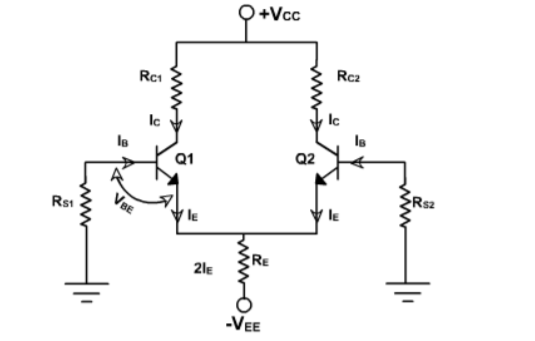
The dc equivalent circuit can be obtained simply by reducing the input signals vin1 and vin2 to zero.
The dc equivalent circuit thus obtained is shown in fig below.
Note that the internal resistances of the input signals are denoted by Rinbecause Rin1 = Rin2.
Since both emitter biased sections of the differential amplifier are symmetrical (matched in all respects), we need to determine the operating point collector current ICQ and collector to emitter voltage VCEQ for only one section.
We shall determine the ICQ and VCEQ values for transistor Q1 only.
These ICQ and VCEQ values can then be used for transistor Q2 also.
Applying Kirchhoff’s voltage law to the base-emitter loop of the transistor Q1,
RinIB- VBE - RE(2IE)+VEE = 0 ---------------------------------------------(1)
But IB = IE/Bdc since IC = IE
Thus the emitter current through Q1 is determined directly from eqn(1) as follows
IE = (VEE - VBE)/(2RE + Rin/Bdc) ---------------------------------(2)
where VBE = 0.6V for silicon transistors
VBE =0.2V for germanium transistors
Generally, Rin/Bdc<< 2RE.Therefore, eqn(2) can be rewritten as
ICQ=IE = (VEE - VBE)/2RE------------------------------------(3)
From eqn(3) we see that the value of RE sets up the emitter current in transistors Q1 and Q2 for a given value of VEE.
In other words, by selecting a proper value of RE, we can obtain a desired value of emitter current for a known value of –VEE.
Notice that the emitter current in transistors Q1 and Q2 is independent of collector resistance RC. Next, we shall determine the collector to emitter voltage VCE. The voltage at the emitter of transistor Q1 is approximately equal to VBE if we assume the voltage drop across Rin to be negligible.
Knowing the value of emitter current IE(=IC),we can obtain the voltage at the collector VCC as follows:
VC = VCC - RCIC
Thus, the collector to emitter voltage VCE is
VCE = VC - VE = (VCC – RCIC) – (-VEE)
VCEQ=VCE = VCC+VBE– RCIC-------------------- (4)
Thus for both transistors we can determine the operating point values by using the eqns (2)and(4), respectively, because at the operating point IE=ICQ and VCEQ=VCE
Due to direct coupling, the dc level at the emitter rises as we move from one stage to another. This can limit the voltage swing and even cause distortions at the output. To counter this, a level shifter is put in use.

It is basically an emitter follower with voltage divider. So a dc voltage at the base of transistor, Q, gives a 0V dc output. This is dependent on resistors R1 and R2. A current mirror bias or a diode current bias can be used in place of the voltage divider emitter follower.
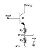
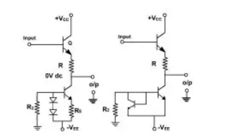
In this case, level shifter, which is a common collector amplifier, shifts the voltage bu 0.7V. But if this is nit enough then the output can be taken at the junction of two resistors in the emitter leg.
When a voltage is supplied to the input of the amplifier circuit it is multiplied by the amplification factor and appears at the output. This amplification factor is obtained by dividing the output voltage by the input voltage.
With an input voltage Vs,and output voltage Vo, the amplification factor Av is defined by the following formula.
AV = | VO |
|
VS |
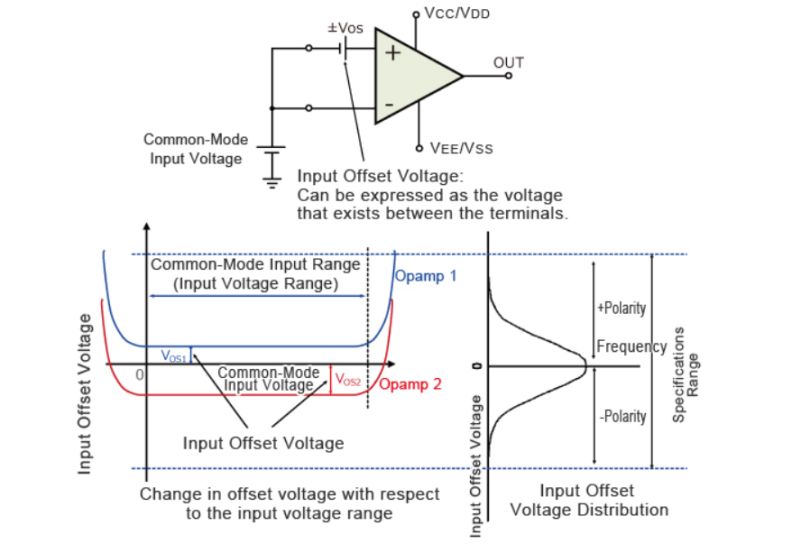
o Input Offset Voltage
With an input offset voltage and a differential input circuit, ideal op-amps and comparators will have an offset voltage of 0V, including error voltage.
When inputting a common-mode (same) voltage to the input pins of an op-amp or comparator, with an ideal op-amp no output voltage will be output
In case where an input offset voltage exists, a voltage will be output based on the input offset voltage. This input offset voltage, which is the differential voltage required to make the output voltage 0V, becomes the input conversion value.
The Offset voltage is normally expressed in units of mV or µV.Values closer to 0 are more ideal.
Slew Rate (SR)
The slew rate is a parameter that describes the operating speed of an op-amp. It represents the rate that can change per unit time stipulated by the output voltage.
For example, 1V/us indicates that the voltage can change by 1V in 1us. Ideal op-amps make it possible to faithfully output an output signal for any input signal. However, in reality slew rate limits do exist.
When supplying a rectangular pulse at the input with a steep rise and fall, this indicates the possible degree of change in the output voltage per unit time.

The rise and fall slew rates are calculated by the following equations:
SRr = ∆ V / ∆ Tr
SRf = ∆ V / ∆ Tf

Calculate the slew rate
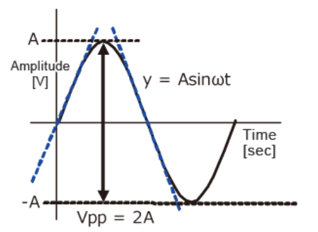
The output is given by
y=Asinωt
The slew rate is the slope of the tangent of the sine wave, differentiating the above equation.
dy | /=Aωcosωt |
| ωt=0 |
Dt |
The slew rate is
SR=Aω ω=2πf
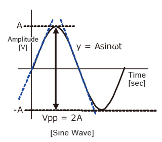
Since the amplitude of the sine wave becomes Vpp=2A (peak-to-peak), the equation can be modified as follows.
|
|
|
|
|
|
|
|
|
This frequency(f) is referred to as the full power bandwidth. These are conditions where the amplification factor in the op-amp has not been set, in other words the relationship of the frequency and amplitude (within the output voltage range) that can be output by the op-amp in a voltage follower circuit.
Negative Feedback System
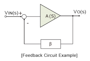
Although op-amps are high voltage gain amplifiers, virtually no op-amps carry out standalone amplification. This is because it is difficult to control the open gain variations and narrow-band amplification factor. Therefore, a negative feedback circuit is typically used.
The basic circuit of the transistor current mirror is shown in the diagram below. It comprises two transistors, one of which has the base and collector connected and the other does not. The base connections of both transistors are then linked, as are the emitters which are also taken to ground.
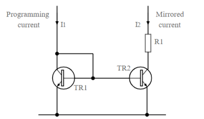
In terms of the operation of the circuit, the base emitter junction of TR1 acts like a diode because the collector and base are connected together.
The current into TRI is set externally by other components, and as a result there is a given voltage built up across the base emitter junction of TR1.
As the base emitter voltage on both transistors is the same, the current in one transistor will exactly mirror that of the second, assuming that both transistors are accurately matched.
Therefore, the current flowing into TR1 will be mirrored into TR2 and hence into the load R1.
In terms of the operation of the circuit, the base emitter junction of TR1 acts like a diode because the collector and base are connected together.
The current into TRI is set externally by other components, and as a result there is a given voltage built up across the base emitter junction of TR1.
As the base emitter voltage on both transistors is the same, the current in one transistor will exactly mirror that of the second, assuming that both transistors are accurately matched. Therefore, the current flowing into TR1 will be mirrored into TR2 and hence into the load R1.
AC characteristics:
Frequency Response:
The variation in operating frequency will cause variations in gain magnitude and its phase angle. The manner in which the gain of the op-amp responds to different frequencies is called the frequency response.
Op-amp should have an infinite bandwidth BW =∞ (i.e.) if its open loop gain in 90dB with dc signal its gain should remain the same 90 dB through audio and onto high radio frequency.
The op-amp gain decreases (roll-off) at higher frequency what reasons to decrease gain after a certain frequency reached. There must be a capacitive component in the equivalent circuit of the op-amp.
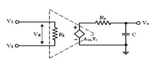
For an op-amp with only one break (corner) frequency all the capacitors effects can be represented by a single capacitor C. Below fig is a modified variation of the low frequency model with capacitor C at the output.

Equivalent circuit of a practical circuit
There is one pole due to R0C and one -20dB/decade. The open loop voltage gain of an op-amp with only one corner frequency is obtained from above fig.
f1 is the corner frequency or the upper 3 dB frequency of the op-amp. The magnitude and phase angle of the open loop volt gain are f1 of frequency can be written as, The magnitude and phase angle characteristics:
1. For frequency f<< f1 the magnitude of the gain is 20 log AOL in db.
2. At frequency f = f1 the gain in 3 dB down from the dc value of AOL in db. This frequency f1 is called corner frequency.
3. For f>> f1 the fain roll-off at the rate off -20dB/decade or -6dB/decade.
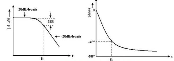
Frequency response of op-amp
From the phase characteristics that the phase angle is zero at frequency f = 0. At the corner frequency f1 the phase angle is -45º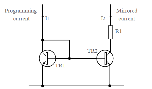
 (lagging and an infinite frequency the phase angle is -90
 . It shows that a maximum of 90
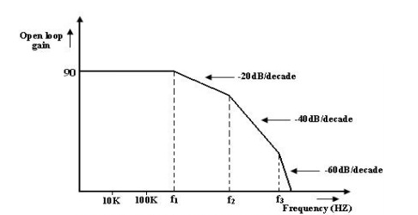 phase change can occur in an op-amp with a single capacitor C. Zero frequency is taken as the decade below the corner frequency and infinite frequency is one decade above the corner frequency.
Roll of rate of op-amp gain
Circuit Stability:
A circuit or a group of circuit connected together as a system is said to be stable, if its o/p reaches a fixed value in a finite time. A system is said to be unstable, if its o/p increases with time instead of achieving a fixed value.
The criterion gn for stability is used when the system is to be tested practically. In theoretically, always used to test system for stability, ex: Bode plots.
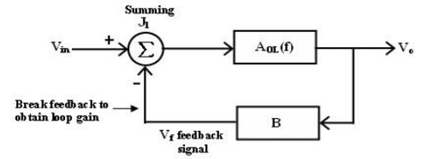
Bode plots are compared of magnitude Vs Frequency and phase angle Vs frequency. Any system whose stability is to be determined can represented by the block diagram.
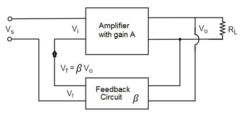
Feedback loop system
The block between the output and input is referred to as forward block and the block between the output signal and f/b signal is referred to as feedback block. The content of each block is referred as transfer frequency.
From fig. we represented it by AOL (f) which is given by
AOL (f) = V0/Vin if Vf = 0 ----- (1)
where AOL (f) = open loop volt gain.
The closed loop gain Af is given by AF = V0/Vin
= AOL / (1+(AOL ) (B) ----(2)
B = gain of feedback circuit.
B is a constant if the feedback circuit uses only resistive components.
Once the magnitude Vs frequency and phase angle Vs frequency plots are drawn, system stability may be determined as follows
1. Method 1:
Determine the phase angle when the magnitude of (AOL) (B) is 0dB (or) 1.
If phase angle is >-180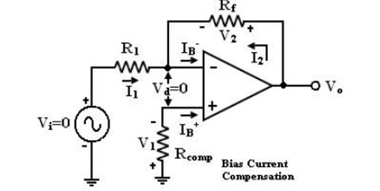 , the system is stable. However, the some systems the magnitude may never be 0, in that cases method 2, must be used.
2. Method 2:
Determine the phase angle when the magnitude of (AOL) (B) is 0dB (or) 1.
If phase angle is > - 180 , If the magnitude is –ve decibels then the system is stable. However, the some systems the phase angle of a system may reach -1800, under such conditions method 1 must be used to determine the system stability.
DC Characteristics of op-amp:
Current is taken from the source into the op-amp inputs respond differently to current andvoltage due to mismatch in transistor.
DC output voltages are,
· Input bias current
· Input offset current
· Input offset voltage
· Thermal drift
Input bias current:
The op-amp‘s input is differential amplifier, which may be made of BJT or FET.
In an ideal op-amp, we assumed that no current is drawn from the input terminals the base currents entering into the inverting and non-inverting terminals (IB- & IB+ respectively).
Even though both the transistors are identical, IB- and IB+ are not exactly equal due to internal imbalance between the two inputs. Manufacturers specify the input bias current IB
If input voltage Vi = 0V. The output Voltage Vo should also be (Vo = 0) but for IB = 500nA We find that the output voltage is offset by Op-amp with a 1M feedback resistor
Vo = 500nA X 1M = 500mV
The output is driven to 500mV with zero input, because of the bias currents.

Current IB+ flowing through the compensating resistor Rcomp, then by KVL we get,
- V1+0+V2-Vo = 0 (or)
Vo = V2 – V1 --------- (1)
By selecting proper value of Rcomp, V2 can be cancelled with V1 and the Vo = 0. The value of Rcomp is derived as
V1 = IB+Rcomp (or)
IB+ = V1/Rcomp ------------------------ (2)
The node ‘a’ is at voltage (-V1). Because the voltage at the non-inverting input terminal is (-V1). So with Vi = 0 we get,
I1 = V1/R1 ------------------------ (3)
I2 = V2/Rf ------------------------ (4)
For compensation, Vo should equal to zero (Vo = 0, Vi = 0). i.e. from equation (3) V2 = V1. So that,
I2 = V1/Rf ——> (5)
KCL at node ‘a’ gives,
IB- = I2 + I1 =( V1/Rf ) +(V1/R1) = V1(R1+Rf)/R1Rf ------------------------ (5)
Assume IB- = IB+ and using equation (2) & (5) we get
V1 (R1+Rf)/R1Rf = V1/Rcomp
Rcomp = R1 || Rf ------------------------ (6)
i.e. to compensate for bias current, the compensating resistor, Rcomp should be equal to the parallel combination of resistor R1 and Rf.
Input offset current:
ü Bias current compensation will work if both bias currents IB+ and IB- are equal.
ü Since the input transistor cannot be made identical. There will always be some small
difference between IB+ and IB-. This difference is called the offset current
|Ios| = IB+-IB------------------------- (7)
Offset current Ios for BJT op-amp is 200nA and for FET op-amp is 10pA. Even with bias current compensation, offset current will produce an output voltage when Vi = 0.
V1 = IB + R comp
And I1 = V1 R1
KCL at node a gives
I2 = (  – I1) =
  - ( Ib+Rcomp/R1 )
Again V0 = I2 Rf – V1
Vo = I2 Rf - IB+ Rcomp
Vo = 1M Ω X 200nA
Vo = 200mV with Vi = 0
Input offset voltage:
In spite of the use of the above compensating techniques, it is found that the output voltage may still not be zero with zero input voltage [Vo ≠ 0 with Vi= 0]. This is due to unavoidable imbalances inside the op-amp and one may have to apply a small voltage at the input terminal to make output (Vo) = 0.
This voltage is called input offset voltage Vos. This is the voltage required to be applied at the input for making output voltage to zero (Vo = 0).
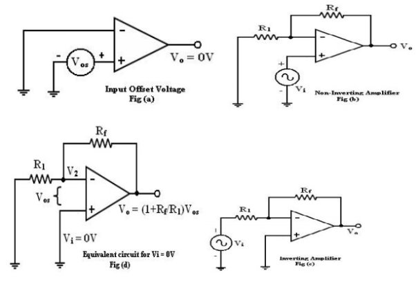
Let us determine the Vos on the output of inverting and non-inverting amplifier. If Vi = 0 (Fig (b) and (c)) become the same as in figure (d).
Voltage-Series Feedback
In the voltage series feedback circuit, a fraction of the output voltage is applied in series with the input voltage through the feedback circuit. This is also known as shunt-driven series-fed feedback, i.e., a parallel-series circuit.
The following figure shows the block diagram of voltage series feedback, by which it is evident that the feedback circuit is placed in shunt with the output but in series with the input.

As the feedback circuit is connected in shunt with the output, the output impedance is decreased and due to the series connection with the input, the input impedance is increased.
Voltage-Shunt Feedback
In the voltage shunt feedback circuit, a fraction of the output voltage is applied in parallel with the input voltage through the feedback network. This is also known as shunt-driven shunt-fed feedback i.e., a parallel-parallel proto type.
The below figure shows the block diagram of voltage shunt feedback, by which it is evident that the feedback circuit is placed in shunt with the output and also with the input.
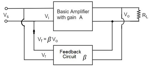
As the feedback circuit is connected in shunt with the output and the input as well, both the output impedance and the input impedance are decreased.
Voltage shunt feedback amplifier:

Voltage gain :
Vo =A.Ii = A(Is – If)
If = β Vo
A(Is – β Vo ) = Vo
A Is = (1+βA ) Vo
Af = Vo/Is = A/ 1+βA
Input Impedance
Zin = Vi/Is = Vi/ Ii + If
= Ii .ri / Ii + βA Ii
Zin = ri / (1+βA)
Output Impedance
Zout IVS =0 = Vo/Io
From input port
Ii = -If = - β Vo
From output port
Io = Vo – A Ii/ro = Vo + βAVo/ro
Zo = Vo /Io = ro/ (1+βA)
Voltage series:
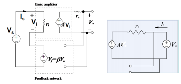
Voltage Gain :
Vo = A.Vi
Vf = β Vo
A(Vs – βVo) = Vo
AVs = (1+βA) Vo
Af = Vo/Vs = A/1+βA
Input impedance
Zin = Vs/Is = Vi+βAVi/Is
Zin = Vi(1+β A ) /Is = ri(1+βA)
Output Impedance
Zout IVS=0 = Vo/Io
Io = Vo – A. Vi / ro
Vi + β.Vo = Vs
Vi = - β Vo
Io = Vo + AβVo/ro
Zout = Vo/Io = ro / 1+Aβ
References:
MOSFET theory and design Book by R. Warner
Operational Amplifiers - Theory and Design Book by Johan H. Huijsing
Fundamentals of Electronics: Book 2: Amplifiers: Analysis and Design Book by Ernest M. Kim and Thomas Schubert
