Unit – 3
Combinational Circuits
Using the Half-Adder and Full-Adder circuits discussed in unit 2, we can design adders and subtractors for n-bit numbers. However, both addition and subtraction can be performed using only adders because the problem of subtraction becomes that of an addition when we use 1’s and 2’s complement representation of negative numbers.
To add 2 n-bit binary numbers, n-Full Adder circuits are needed that will produce a (n+1) bit binary number as the SUM. The circuit and block diagram of a n-bit adder using Full-Adders is shown in Fig a and b respectively:
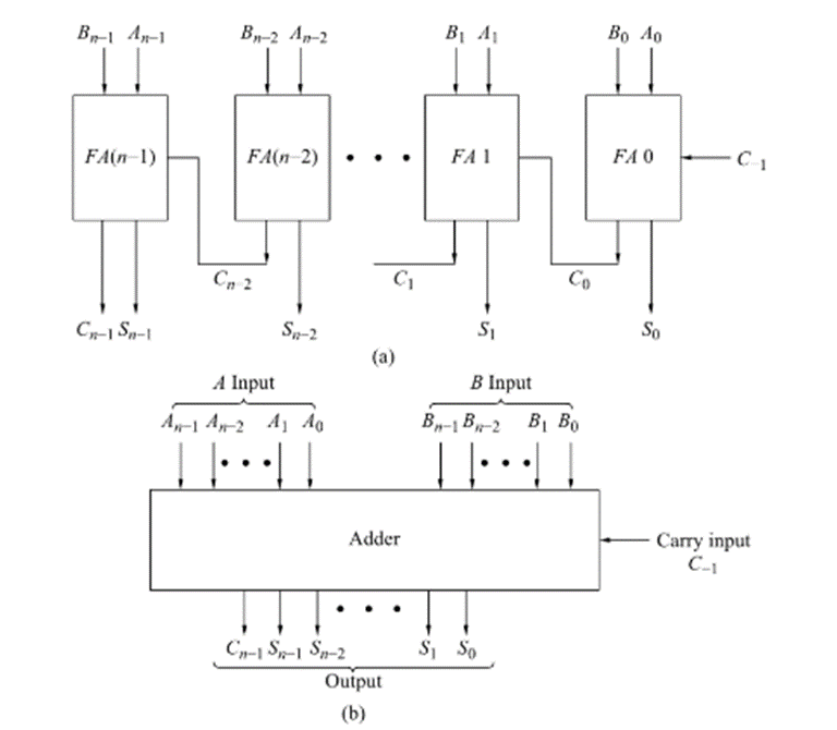
A and B are the two n-bit inputs to be added and Cn-1 , Cn-2 , Sn-2 , ..... S2, S1, S0 is their sum. A half-adder may be used to add the least significant bits A0 and B0. However, for cascading these adders to increase the number of bits to be added, the CARRY input terminal is required for the adder to add the least significant bits. Hence all the adders used are Full-Adders.
In the above circuit (a), the sum S0 and Carry C0 outputs are delayed because of the propagation delays of the gates involved in FA0. The S0 output however is the LSB of the final result and it is not required to be passed through other gates and hence does not get further delayed. The carry output C0 acts a carry input of the full-adder FA1 and therefore the outputs of FA1 – S1 and C1 will reach steady state only after the arrival of C0 and propagation delay introduced by FA1. This means that the total delay up to FA1 will be the sum of delays introduced by FA0 and FA1. Similarly going further in the chain of adders towards MSB, the carry has to ripple down the line of cascaded adders.
This decreases the operating speed of the adder as the number of adder stages is increased. To overcome this disadvantage, a Look Ahead Carry Adder is used.
Consider the full-adder circuit in block diagram form and its EX-OR realization is shown in fig (a) and (b) below:

The output Gi of the first half-adder is 1if Ai and Bi both are 1 and a carry is generated. The variable Gi is known as ‘Carry Generate’ and can be expressed as:
Gi = Ai Bi -------- (1)
The variable Pi known as ‘Carry Propagate’ because a carry in may be propagated by the full-adder when either or both of the input bits are 1. This condition is expressed as the OR function of A and B:
Pi= A+B -------- (2)
Therefore Si and Ci can be written as:
Si= Pi  Ci -1 = Ai
  Bi
Bi  C i -1 ---------- (3)
Ci = Gi + Pi Ci – 1 ----------- (4)
Using equation (4), the Boolean expression for carry output of each stage can be written as:
Ci +1 = Gi +1 + Pi+1 . Ci
Substituting the value of Ci from equation 4, we obtain:
C i+1 = G i+1 +P i+1 . Gi +P i+1P C i-1
For a 4 bit adder, the Boolean expressions for the carry outputs C0, C1, C2 and C3 can be obtained as:

Similarly for an n-stage adder, the final carry C n-1 can be determined.
By observing the above equations, the logic variables involved are:
G0, G1, G2, G3, P0, P1, P2, P3 and C-1
The G variables can be generated directly from A and B inputs using AND gates. The P variables are obtained directly from A and B inputs using EX-OR gates. C-1 is the carry input. If G’s , P’s and C-1 are available simultaneously, the carry outputs C0, C1, C2, C3 are produced by using 2-level realization. Therefore for the generation of these carry outputs, propagation delay time of two gates only wi;; be there. These carry outputs are connected to the carry inputs of the succeeding stages, thereby eliminating the problem of carry rippling through all the stages.
The logic circuit of a Look-Ahead Carry Adder can be realized using the above equations. A 4-bit adder with look-ahead carry is shown below:
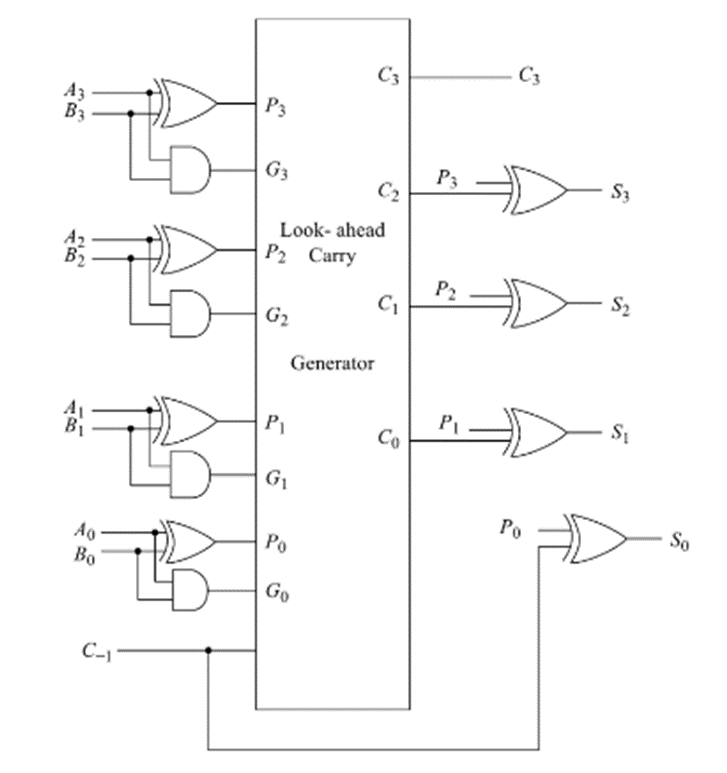
Thus we can see that by generating all the individual carry terms needed by each full adder in a 2-level circuit, the propagation delay time through the adder is considerably reduced and it becomes independent of the number of full-adders in the circuit.
ALU is the most widely used combinational circuit that is capable of performing arithmetic as well as logical operations. The following figure gives the block diagram of ALU:
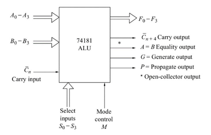
The functions of various input, output and control lines are given below:
A and B: 4- bit binary data input
 n : Carry input (active low)
F : 4-bit binary data output
 n+4 : Carry output (active low) – For subtraction operation, it indicates the sign of the output. Logic 0 indicates positive result and logic 1 indicates negative result expressed in 2’s complement form.
A=B : Logic 1 on this line indicates A=B
G : Carry generate output
P : Carry Propogate output
Select input(S) : Used to select any operation(refer table below)
Mode control(M) : M=0 Arithmetic operations
M=1 Logic Operations
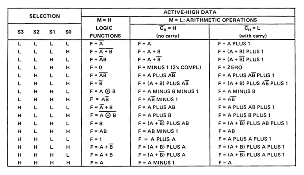
Following is the function table of the 74181 ALU:
Example: Design an 8-bit adder/subtractor using 74181s in cascade. Show how it works for A=97 and B=29
Solution: The least significant 4-bits of A and B are applied at the A and B inputs of the least significant 74181 and the most significant 4-bits of A and B are applied at the A and B inputs of the most significant 74181. The carry out of the least significant 74181 is connected to the carry-in of the most significant 74181. The 8-bit output will be available on F outputs. The select lines of both the 74181s are connected together.
Addition is performed with M=0 and =1001, and subtraction is performed with M=0 and S=0110. Connect  n of least significant 74181 to 1 for addition and 0 for subtraction.
Therefore for A= 97 (01100001) and B=29(00011101)

A comparator is a logic circuit, used to compare the magnitude of two binary numbers.
The following figure shows the block diagram of a n-bit comparator.
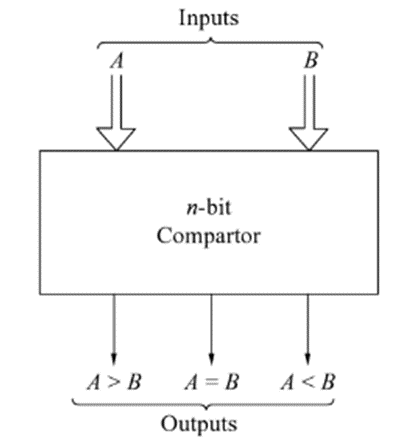
It receives two n-bit numbers A and B as inputs and the outputs are A>B,A=B and A<B. Depending upon the relative magnitude of the two numbers, one of the outputs will be high.
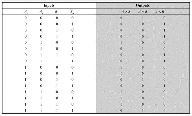
The following is the truth table of a 2-bit comparator.
Binary data when transmitted and processed, is susceptible to noise that can alter its 1’s to 0’s and 0’s to 1’s. To detect such errors, an additional bit called the parity bit is added to data bits and word containing data bits and the parity bit is transmitted. At the receiving end, the numbers of 1’s in the word received are counted and the error, if any, is detected. This parity check, however detects only single bit errors.
The circuits for the generation of parity bits and checking the parity of a given word can be designed using gates. But because of wide use, an 8-parity generator/ checker circuit has been designed and is available as IC 74180.
The following figure gives the block diagram of 74180 in which there are 8 parity inputs A through H and two cascading inputs. There are two outputs ∑EVEN and ∑ODD.
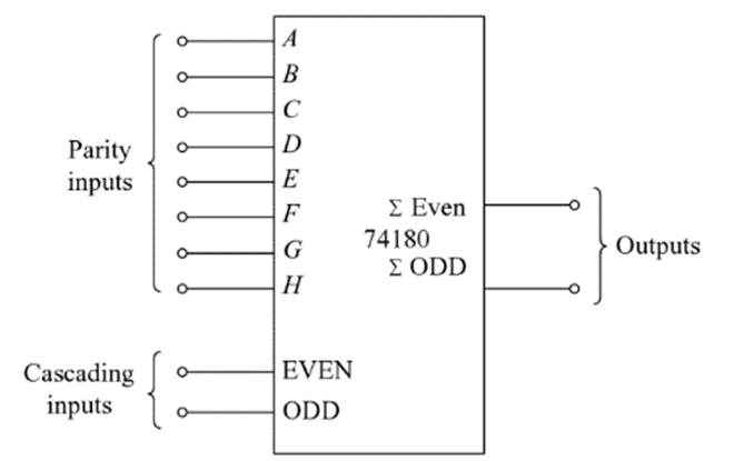
74180 can be used as parity generator as well as parity checker. Its function as a parity checker can be understood from its function table given below:

Its function as a parity generator is given in the table below:

The cascading inputs must not be equal and the unused parity bits must be tied to logic 0 level.
MULTIPLEXER
Multiplexing means sharing. A multiplexer (MUX) or data selector is a logic circuit that accepts several data inputs and allows only one of them at a time to get through to the output. The routing of the desired data input to the output is controlled by SELECT lines. Block diagram of a MUX with n inputs and one output is shown below:
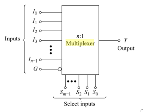
For selecting one out of n inputs for connection to the output, a set of m select inputs is required, where 2m =n. Depending upon the digital code applied at the select inputs, one out of the n-data sources is selected and transmitted to a single output channel.
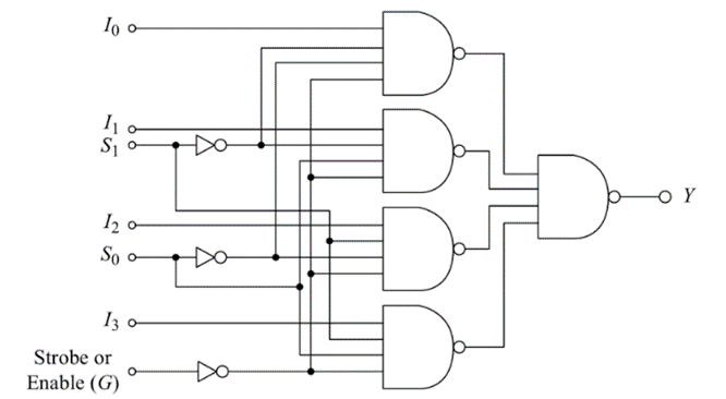
Normally, an ENABLE input G is incorporated which helps in cascading and is generally active-low. The following is the truth table of a 4:1 MUX with active low enable input G:

Its output Y can be expressed as: 
The above equation can be realized using NAND Gates as shown below:
COMBINATIONAL LOGIC DESIGN USING MULTIPLEXERS
Multiplexers find numerous applications in digital systems of all types. These applications include data selection, data routing, operation sequencing, parallel to serial conversion, waveform generation and logic function generation.
LOGIC FUNCTION GENERATOR
The multiplexing function discussed above can conveniently be used a logic element in the design of combinational circuits. Use of Multiplexers in the design of combinational circuits has the following advantages:
For using the MUX as a logic element, either the truth table or one of the canonical forms of logic expression must be available. The design procedure is given below:
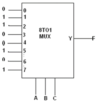
1) Identify the decimal number corresponding to each minterm in the expression. The input to these numbers is to be connected to logic 1 level.
2) All other input lines are to be connected to logic 0 level.
3) The inputs are to be applied to select inputs.
Example 1: Implement the expression F=∑m(1,2,5,7) uisng a multiplexer.
Solution: Since there are 3 variables, an 8:1 MUX (3 select inputs) is required. This implementation requires only one IC package. In case the output of the multiplexer is active low, the logic 0 and logic 1 inputs are to be interchanged.
Example 2: Realize the logic function of the truth table given below using 8:1 MUX
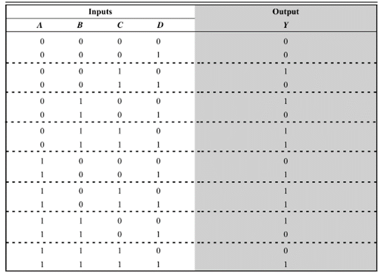
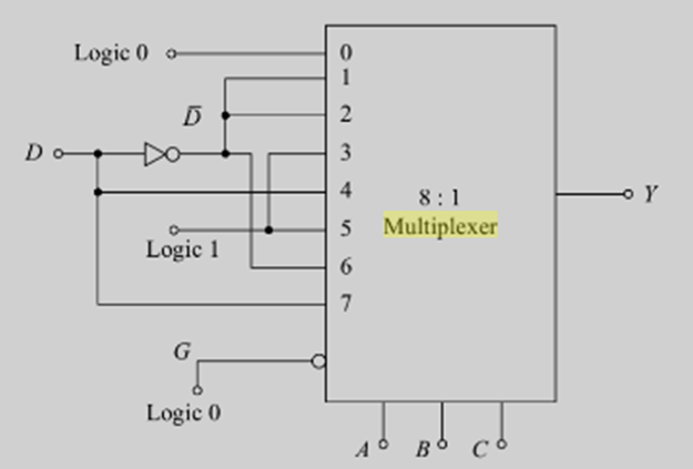
Solution: A 4 variable truth table or logic expression can be realized by using an 8:1 MUX instead of a 16:1 MUX. For this, we need to partition the truth table shown by dotted lines. The inputs A, B and C are connected to the SELECT inputs. The relationship between the input D and output Y for each group of two rows can be observed in the above table. These are given in the table below:
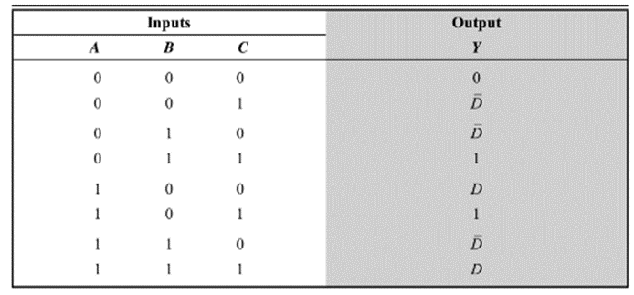
Note the output Y for each of the combinations of A,B and C and make the connections accordingly. The implementation of this function using an 8:1 MUX is shown below:
Since 16:1 MUX are the largest available IC’s, therefore to meet the larger input needs there should be a provision for expansion. This is achieved with the help of enable/ strobe inputs. Two commonly used methods for this purpose are explained below:
METHOD 1
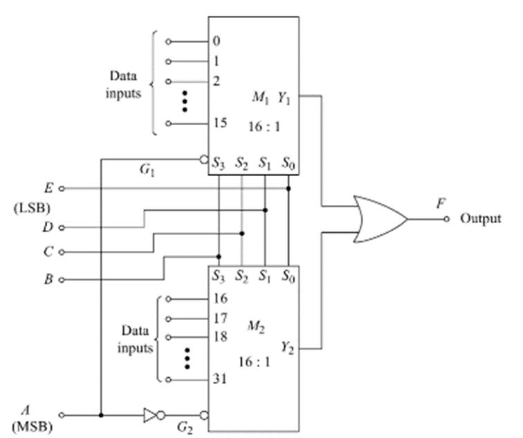
This circuit uses two 16:1 MUX’s for the realization of a 32:1 MUX. The lower order 16 data input lines are applied at the data input terminals of the Multiplexer M1 and the higher order 16 data input lines are applied at the data input terminals of the Multiplexer M2. The number of select lines required for 32:1 MUX is 5. The select inputs are A,B,C,D and E. Select input A is applied at G1 and  is applied at G2. B,C,D,E are connect to S3, S2, S1 and S0 inputs of both the multiplexers. The output F of the multiplexer is obtained by using an OR gate.
When A=0, M1 is enabled and M2 is disabled, thereby allowing one of the lower order 16 bits to Y1, depending upon the value of BCDE, Y2=0. Therefore F=Y1. Similarly, when A=1, M2 is enabled and M1 is disabled and F=Y2.
METHOD 2
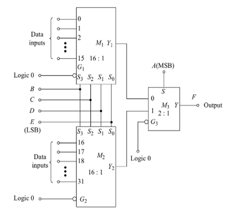
This circuit uses a 2:1 MUX instead of an OR gate. When A=0, F=Y1 and when A=1, F=Y2. Thus, both the circuits perform similar operation.
These two general techniques can be used to expand to an n-input multiplexer.
DEMULTIPLEXER
The demultiplexer performs the reverse operation of a multiplexer. It accepts single input and distributes it over several outputs. So, a Demultiplexer can be thought of as a ‘distributor’, since it transmits the same data to different destinations. The SELECT input code determines to which output the data will be transmitted. The block diagram of a demultiplexer is shown below:
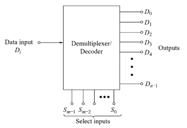
The number of output lines is n and the number of select lines is m where n=2m. The data input D will appear on the output line selected by the SELECT input. Eg: if the decimal equivalent of the select input is 4, then the data will appear on D4 output line. This circuit can also be used as binary-decimal decoder with binary inputs applied at the select input lines and the output will be obtained on the corresponding line. The data input line is to be connected to logic 1 level.
Unlike the MUX, the decoder requires some gates inorder to realize Boolean expressions in the canonical SOP form. Consider the following example:
Implement the following multi-output combinational logic circuit using 4-to-16 line decoder
F1=∑m(1,2,4,7,8,11,12,13)
F2=∑m(2,3,9,11)
F3=∑m(10,12,13,14)
F4=∑(2,4,8)
Solution: The 4-bit input ABCD is applied at the select input terminals S3,S2,S1 and S0. The output F1 is required to be 1 for minterms 1,2,4,7,8,11,12 and 13. Therefore a NAND Gate is connected as shown (since the output is active LOW). Similarly NAND gates are used for the outputs F2,F3 and F4.( If the decoders output was not active low, OR gate can be used instead of NAND gate)
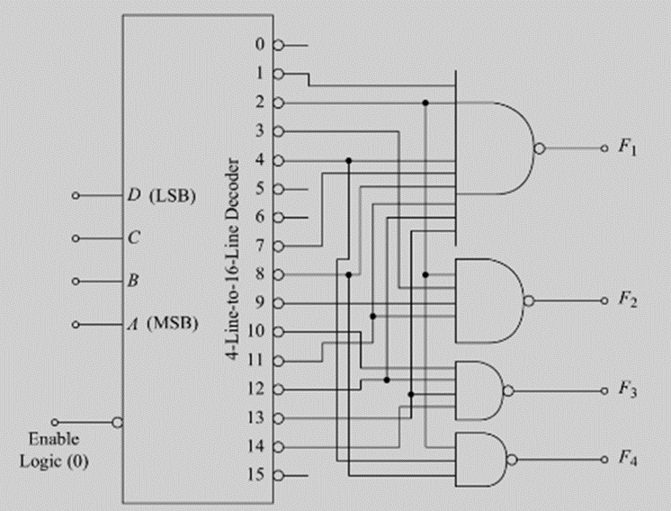
In the combinational logic design using MUX, additional gates are usually not required, whereas design using demultiplexer requires additional gates. However even with this disadvantage, the decoder is more economical in cases where n-trivial, multiple output expressions of the same input variables are required. In such cases, one multiplexer is required for each output whereas it is likely that only one decoder will be required, supported with a few gates. Therefore, using a decoder could have advantages over using a MUX.
Since 4-line to 16-line decoders are the largest available circuits in IC’s, for larger inputs, the ENABLE input terminal is used for expansion.
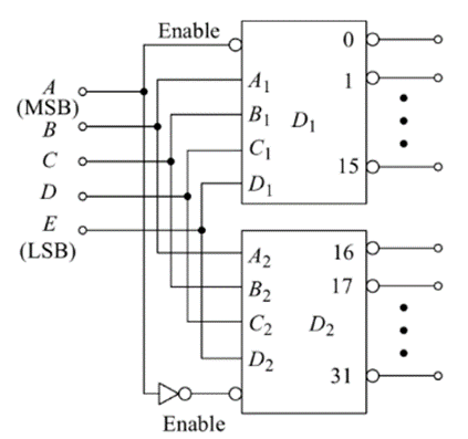
Fig: 5-line to 32-line decoder using two 4-line to 16-line decoders
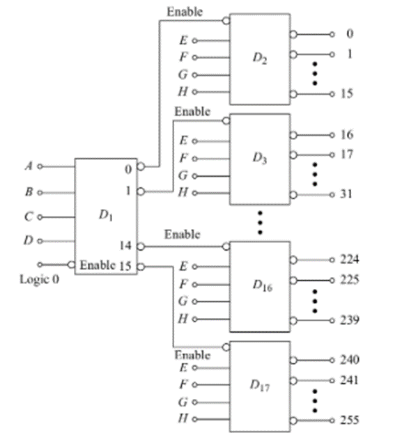
Fig: 8-line to 256-line decoder using 4-line to 16-line decoders
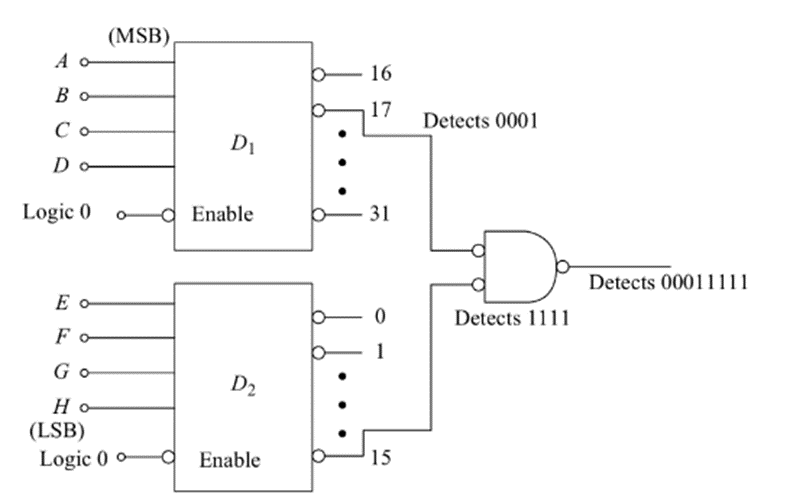
In a similar way, any m-line to n-line decoder can be implemented. However if only a few codes of a large number need to be recognised, an alternative approach as shown below can be used. This circuit has been connected to detect the digital number 00011111. The most significant 4 bits are applied at A,B,C,D inputs and the least significant bits are applied at E,F,G,H inputs. The output goes low when MS bits are 0001 and the LS bits are 1111. This circuit can be expanded to detect other 8-bit codes.
