Unit 4
Pulse Modulation
Analog signals are a type of continuous signals which are time-varying. Most of the environmental sensors such as temperature, light, pressure, and sound sensors communicate with microcontrollers using analog signals. These analog sensors output values in a specific range based on what the sensors are sensing. Analog signals normally take the form of sine waves and they can be defined by amplitude, frequency, and phase where amplitude denoting the highest height of the signals, frequency denoting the varying rate of the analog signals and phase denoting the position of the signal in time.
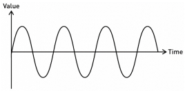
Figure 1. Analog signal
Digital signals are a type of discrete signals which are time-varying. The data is carried in the form of binary in a digital signal. This means it can either carry a “0” or a “1”. If you think about a switch, it sends out digital signals when pressing it to turn on while transmitting as a “1” and when pressed again to turn off while transmitting as a “0”. Digital signals also have an amplitude, frequency, and a phase just like analog signals. Digital Signals are normally defined by bit interval and bitrate where bit interval is the required time to transmit one bit and bitrate is the frequency of the bit interval.
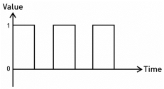
Figure 2. Digital Signal
When you need to use analog sensors and communicate with a microcontroller, it is not possible for the microcontroller to directly understand these analog signals because microcontrollers only understand digital signals which are formed by 1’s and 0’s. Therefore, this kind of system needs an intermediate device that could convert the analog signals from these sensors to digital signals in order for the microcontroller to understand these signals. An ADC (Analog to Digital Converter) is an electronic integrated circuit which is able to convert these analog signals to digital signals.
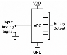
Figure 3: ADC
Normally an ADC would accept a range of voltage inputs and convert those into a form of binary numbers.
Key Takeaways:
- Analog signal
- Digital signal
- Need for analog to digital conversion
Statement: - “If a band –limited signal g(t) contains no frequency components for ׀f׀ > W, then it is completely described by instantaneous values g(kTs) uniformly spaced in time with period Ts ≤ 1/2W. If the sampling rate, fs is equal to the Nyquist rate or greater (fs ≥ 2W), the signal g(t) can be exactly reconstructed.
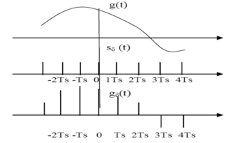
Figure4. Sampling process
Given a band-limited analog lowpass signal xa (t) — that is, the highest frequency component of xa (t) is strictly less than a given upper bound, say B /2 — then xa (t) can be suitably represented by a discrete signal x(n) made up of uniformly spaced samples collected at a minimum rate of B samples per second. B is known as the Nyquist rate. Inversely, given the discrete samples x(n) sampled at least at the Nyquist rate, the original analog signal xa (t) can then be reconstructed without loss of information.
The Fourier transform of an analog signal xa (t) is expressed as
Xa(F) =  e -j2πFt dt ------------------------------------------(1)
The analog time domain signal can be recovered from Xa (F) via the inverse Fourier transform as:
Xa(t) = =  e j2πFt dF------------------------------------------------(2)
Next, consider sampling xa (t) periodically every Ts seconds to obtain the discrete sequence:
x(n) = xa(t) | t=nTs =xa(nTs) -------------------------------------------------(3)
The spectrum of x(n) can then be obtained via the Fourier transform of discrete aperiodic signals as:
X(f) =  e -j2πfn --------------------------------------------------------(4)
Similar to the analog case, the discrete signal can then be recovered via the inverse Fourier transform as:
x(n) =  e j2πfn df -----------------------------------------------------(5)
To establish a relationship between the spectra of the analog signal and that of its counterpart discrete signal, we note from (2) and (3) that:
x(n) = xa(nTs) =  e j2πf/Fsn df --------------------------------------------(6)
Note that from (6), periodic sampling implies a relationship between analog and discrete frequency f = F/Fs, thus implying that when comparing (5) and (6) we obtain:
 e j2πfn df | f=F/F = 1/Fs
 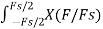 e j2πF/Fsn df --------------(7)
Df = dF/Fs
The integral on the right-hand side of (7) can be written as the infinite sum of integrals:
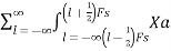
 e j2πF/Fsn dF =
  (F) e j2πF/Fsn dF --------------(8)
Recognizing that Xa (F ) in the interval ((l – 1/2) Fs , (l + 1/2) Fs ) is equivalent to Xa (F + lFs ) in the interval(-Fs / 2, Fs / 2s ) , then the summation term on the right hand side of (8) becomes:
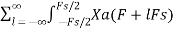
 (F) e j2πF/Fsn dF =
  e j 2π F+lFn/Fs dF-----(9)
Swapping the integral and the summation sign on the right-hand side of (9), and noting that:
e j2π F+lFs/Fs .n = e j2π lFs/Fs .n . e j2π F/Fs .n = e j2π F/Fs .n --------------------------(10)
We obtain:
 e j 2π F+lFn/Fs dF =
 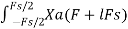 e j 2π Fn/Fs dF -----(11)
Comparing (7) and (11) we obtain:
1/Fs  e j 2π F/Fs.n dF =
  e j 2π F/Fs n dF----(12)
And hence, from (12), one can deduce the relation:
X(F/Fs) = Fs  or
or
X(f) = Fs  Fs -----------------------------------------------------(13)
The relation in(13) implies that the spectrum of X(f) is made up of replicas of the analog spectrum Xa (F) periodically shifted in frequency and scaled by the sampling frequency Fs as shown in Figure.
The relationship in (13) expresses the association between the analog spectrum and its discrete counterpart. The discrete spectrum is essentially made up of a series of periodic replicas of the analog spectrum. If the sampling frequency Fs is selected such that Fs ≥B, where B is the IF bandwidth not to be confused with the baseband bandwidth, which is only the positive half of the spectrum, the analog signal can then be reconstructed without loss of information due to aliasing from the discrete signal via filtering scaled by Fs.
Note that the minimum sampling frequency allowed to reconstruct the analog signal from its discrete-time counterpart is Fs =B. This frequency is known as the Nyquist rate.
However, if Fs is chosen such that Fs < B, then the reconstructed analog signal suffers from loss of information due to aliasing, as shown in Figure (c) and (d), and an exact replica of the original analog signal cannot be faithfully reproduced. In this case, as can be seen from Figure (c), the discrete spectrum is made up of scaled overlapped replicas of the original spectrum Xa (F) . The reconstructed signal is corrupted with aliased spectral components coexisting on top of the original spectral components as can be seen in Figure (d), thus preventing us from recreating the original analog signal.
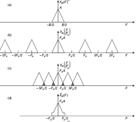
Figure 5. Lowpass sampling of analog signals: (a) spectrum of analog bandlimited signal, (b) spectrum of discrete-time sampled analog signal scaled by Fs and replicated, (c) aliased spectrum of discrete-time sampled signal, and (d) spectrum of reconstructed analog signal derived from aliased discrete-time signal in (c).
Reconstruction of Lowpass Signals
The Fourier transform of the analog signal xa (t) is:
Xa(t) =  e j2πft dF ---------------------------------------(14)
Assume for simplicity's sake that the discrete-time signal is sampled at the Nyquist rate Fs = B, that is:
Xa(F) = { 1/Fs X(F/Fs) – Fs/2 <F<Fs/2--------------------------------(15)
0 otherwise
Substituting the relation of (15) into (14) we obtain
 = 1/Fs
  e j2πft dF ----------------------------------------(16)
Where  a (t) is the reconstructed analog signal.
Recall that the Fourier transform of  is given as:
X(F/Fs) =  e -j2π F/Fs n -------------------------------(17)
Where Ts is the sampling rate. Substituting (17) into (16), it becomes:
 = 1/Fs
  e -j2πF/Fsn dF. e j2π Ft dF ---------------------(18)
Rearranging the order of the summation and integral in (18):
 =
=  { 1/Fs
  e -j2πF(t-n/Fs) dF --------------------------(19)
The integral in (19) is the sinc function:
1/Fs  e -j2πF(t-n/Fs) dF = 1/Fs e j2πFs/2(t-n/Fs) – e -j2πFs/2(t-n/Fs) / j2π(t-n/Fs) =
= sin(2πFs/2(t-n/Fs))/ π(t-n/Fs)-------------------------------------(20)
1/Fs  j2πF(t-n/Fs) dF | Ts = 1/Fs = sin(π/Ts (t-nTs)/ π/Ts(t-nTs)-----(21)
The reconstructed analog signal in (7.21) involves weighing each individual discrete sample by a sinc function shifted-in-time by the sampling period. The sinc function:
p(t) = sin( π/Ts(t-nTs)]/ π/Ts(t-nTs)--------------------------------------------(22)
Is known as the ideal interpolation filter expressed in the frequency domain as:
P(F) = { 1 |F| < Fs/2
0 |F|  Fs/2 --------------------------------------------------(23)
Applying the ideal interpolation filter in (7.23) to the spectrum of a non-aliased discrete-time signal results in recovering the original analog signal without any loss of information, as shown in Figure.
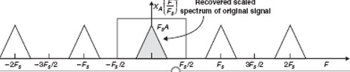
Figure6. Recovered sampled spectrum of original analog signal.
Therefore, another simple way to arrive at the relationship expressed in (7.21) is to start with filtering the spectrum of the discrete-time signal by the interpolation filter (7.23), that is:
 (F/Fs) = X(F/Fs) P(F)-----------------------------------------------------------(24)
Multiplication in the frequency domain is convolution in the time domain,
 * p(t) =
  sin(
sin( (t-nTs))/
  (t-nTs) ------(25)
Which is none other than the relationship developed in 21.
Note that certain modulation schemes require a flat response at the output of the DAC. Hence, the in-band distortion due to the weighing function of the sinc must be corrected for. This is typically done with an equalizer mimicking an inverse sinc filter.
Nyquist rate:
Nyquist rate is the rate at which sampling of a signal is done so that overlapping of frequency does not take place. When the sampling rate become exactly equal to 2fm samples per second, then the specific rate is known as Nyquist rate. It is also known as the minimum sampling rate and given by: fs =2fm
Key Takeaways:
- Definition of sampling theorem
- Derivation
- Reconstruction of the sampled signal
Natural and flat top
Natural sampling is similar to impulse sampling, except the impulse train is replaced by pulse train of period T. That is you multiply input signal x(t) to pulse train

As shown below

Figure 7. Natural Sampling
The output of sampler is
y(t)=x(t)×pulse train
=x(t)×p(t)
=x(t)×  -----------------------(1)
The exponential Fourier series representation of p(t) can be given as
p(t)=  ejnωst......(2)
= ej2πnfst......(2)
Where Fn = 1/T  e -jnwst dt
= 1/TP (nws)
Substitute Fn value in eq(2)
p(t)=  ejnwst
= 1/T  ejnwst
Substitute Fn value in eq(1)
y(t) = x(t) x p(t)
= x(t) x 1/T  (nws) e jnwst
y(t) = 1/T  e jnwst
To get the spectrum of the sampled signal consider the Fourier transform on both sides
F.T [ y(t)] = F.T [ 1/T  x(t) e jnwst ]
= 1/T  F.T [x(t) e jnwst]
According to frequency shifting property
F.T [ x(t) e jnwst] = X[w-nws]
Y[w] = 1/T  X[w-nws]
Flat Top Sampling
During transmission, noise is introduced at top of the transmission pulse which can be easily removed if the pulse is in the form of flat top. Here, the top of the samples is flat i.e. they have constant amplitude. Hence, it is called as flat top sampling or practical sampling. Flat top sampling makes use of sample and hold circuit.
Theoretically, the sampled signal can be obtained by convolution of rectangular pulse p(t) with ideally sampled signal say yδ(t) as shown in the diagram:
i.e. y(t)=p(t)×yδ(t)......(1)
Figure 8. Flat top sampling
To get the sampled spectrum, consider Fourier transform on both sides for equation 1
Y[ω]=F.T[P(t)×yδ(t)]
By the knowledge of convolution property,
Y[ω]=P(ω)Yδ(ω)
Here P(ω)=TSa(ωT/2)=2sinωT/ω
Key Takeaways:
- Natural Sampling and its derivation
- Flat top sampling and its derivation
Pulse Amplitude Modulation (PAM): In pulse amplitude modulation, the amplitude of regular interval of periodic pulses or electromagnetic pulses is varied in proposition to the sample of modulating signal or message signal. This is an analog type of modulation. In the pulse amplitude modulation, the message signal is sampled at regular periodic or time intervals and this each sample is made proportional to the magnitude of the message signal. These sample pulses can be transmitted directly using wired media or we can use a carrier signal for transmitting through wireless.
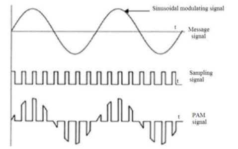
Figure9.PAM Signal
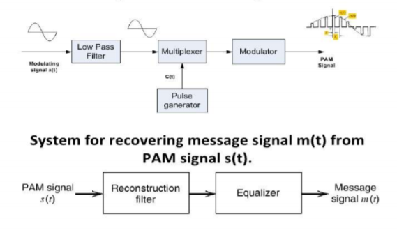
Figure 10. Block diagram for PAM generation
Concept of TDM:
In TDM, the data flow of each input stream is divided into units. One unit may be 1 bit, 1 byte, or a block of few bytes. Each input unit is allotted an input time slot. One input unit corresponds to one output unit and is allotted an output time slot. During transmission, one unit of each of the input streams is allotted one-time slot, periodically, in a sequence, on a rotational basis. This system is popularly called round-robin system.
Example
Consider a system having four input streams, A, B, C and D. Each of the data streams is divided into units which are allocated time slots in the round – robin manner. Hence, the time slot 1 is allotted to A, slot 2 is allotted to B, slot 3 is allotted to C, slot 4 is allotted to D, slot 5 is allocated to A again, and this goes on till the data in all the streams are transmitted.
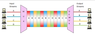
Figure 11. TDM
Key Takeaways:
- PAM signal
- Generation of PAM signal
- Concept of TDM
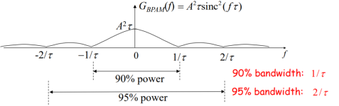
Figure 12. Bandwidth PAM
Suppose 90% of signal power must pass through the channel (90% in-band power):
Required channel bandwidth: Bh-90% = 1/τ
Bit rate Rb = 1/τ
Suppose 95% of signal power must pass through the channel (95% in-band power):
Required Channel Bandwidth: Bh_95% = 2 / = 2Rb
Bandwidth Efficiency =  Information Bit rate Rb/ Required Channel Bandwidth
Bandwidth Efficiency of Binary PAM:
Rb = 1/τ
Bh_90% = 1/τ
Bh_95% = 2/τ
Equalization:
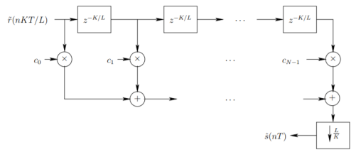
Figure 13. Equalization
A fractionally spaced equalizer also acts as an interpolator and automatically adjusts for signal time shifts. The receiver symbol clock must be locked in frequency to the transmitter clock. If there is a clock frequency difference, the equalizer will compensate for the drifting clocks and will fail when the correct timing falls off its ends.
The equalizer is an FIR filter with a delay line and taps spaced TK/L = T /Q which is T /2 for our experiments. A block diagram of the equalizer is shown if Figure . The blocks labeled z −K/L represent delays of KT /L = T /Q. It is said to be a fractionally spaced equalizer. • The equalizer output is computed once per symbol and gives an estimate ˆs(nT) of the transmitted symbol
Signal Recovery through holding:
Holding (lengthening): achieved by applying the sampled signal to a time-invariant filter with unit impulse response.
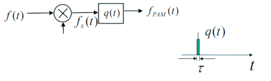
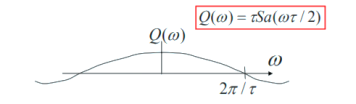
Figure 14. Signal Recovery
f PAM (t) = fs(t) x q(t)
= [ f(t) pT(t) x q(t)
= f(t)  x q(t)
=  q(t-nT)
The spectral density of PAM signal is
F PAM(w) = F{fs(t) x q(t)}
= Fs(w) Q(w)
= 1/T 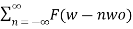 Q(w)
Q(w)
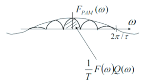
Figure 15. Spectral Density PAM
Key Takeaways:
- Channel bandwidth of PAM
- Spectral density of PAM
- Equalization
Pulse Width Modulation (PWM):
It is a type of analog modulation. In pulse width modulation or pulse duration modulation, the width of the pulse carrier is varied in accordance with the sample values of message signal or modulating signal or modulating voltage. In pulse width modulation, the amplitude is made constant and width of pulse and position of pulse is made proportional to the amplitude of the signal. We can vary the pulse width in three ways
1. By keeping the leading-edge constant and vary the pulse width with respect to leading edge
2. By keeping the tailing constant.
3. By keeping the center of the pulse constant.
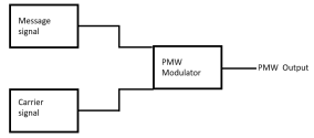
Figure 16. Block diagram of PWM
Pulse width Demodulation
Figure 17. Pulse width Demodulation
Pulse position modulation (PPM):
In the pulse position modulation, the position of each pulse in a signal by taking the reference signal is varied according to the sample value of message or modulating signal instantaneously. In the pulse position modulation, within and amplitude is kept constant. It is a technique that uses pulses of the same breath and height but is displaced in time from some base position according to amplitude of the signal at the time of sampling. The position of the pulse 1:1 which is propositional to the width of the pulse and positional to the instantaneous amplitude of samples modulating signal. The position of pulse position modulation is easy when compared to other modulation. It requires pulse width generator and monostable multivibrator.
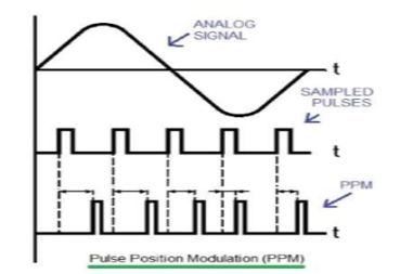
Figure 18. PPM
Pulse width modulation signal which will help to trigger the monostable multivibrator, here trial edge of PWM signal is used for triggering the monostable multivibrator, PWM signal is converted into pulse position modulation signal. For demodulation, it requires reference pulse generator, flip-flop width modulation and demodulator.
Generation of PPM Signal
1. The PPM Signal can be generated from PWM signal. The PWM pules obtained at the comparator
Output are applied to a mono stable multivibrator
2. Hence corresponding to each trailing edge of PWM signal, the mono stable output goes high. It remains high for a fixed time decided by its own RC comparator.
3. Thus as the trailing edges of the PWM signal keep shifting in proportion with the modulating
Signal x(t), the PWM pulses also keep shifting
4. All the PPM pulses have the same with and amplitude. The information is conveyed via changing
The portion of pulses.
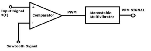
Figure 19. Generation of PPM Signal
Demodulation of PPM
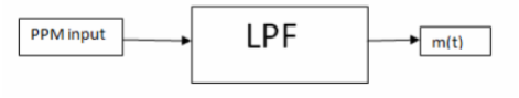
Figure 20. Demodulation of PPM
Key Takeaways :
- PWM and its generation
- PPM and its generation
References:
- Digital Communication Systems Book by Simon S. Haykin
- Principles of digital communication Textbook by Robert G. Gallager
- Digital Communications Book by John G Proakis and Masoud Salehi
- Digital Communications Book by Sanjay Sharma
- Digital Communication Book by J.S.Chitode


