Unit - 1
Introduction to Microcontroller Architecture
| Microprocessor | Microcontroller |
System | It is the heart of the computer system, | It is the heart of an embedded system. |
Contains | It contains CPU, general purpose registers, stack pointers, program counters, clock timing and interrupt circuits. | It contains the circuitry of microprocessor and has built-in ROM, RAM, I/O devices, timers and counters. |
Data memory | It has many instructions to move data between memory and CPU | It has one or two instructions to move data between memory and CPU. |
Circuit | It is large | It is small |
Cost | Cost of the entire system increases | Cost of the entire system is low. |
Bit instructions | It has one- or two-bit handling instructions. | It has many bit handling instructions |
Register numbers | It has less number of registers; hence the operations are memory based. | It has more number of registers; hence the programs are easier to write. |
Storage | It is based on Von Neumann architecture, where the program and data are stored in the same memory module. | It is based on the Harvard architecture, where the program memory and data memory are stored in separate module |
Time | Access time for memory and I/O devices is more. | Less access time for built-in memory and I/O devices. |
Hardware | It requires more hardware | It requires less hardware. |
Basically, a microcontroller is classified based on the following categories listed below
Based on Memory
Depending upon the type of memory it is classified as External memory microcontroller and Embedded Memory Microcontroller. For external memory microcontroller we need to provide external program memory as the microcontroller does not have any on chip memory. On the other hand, Embedded memory microcontroller has on chip program and data memory. These controllers have I/O ports, timer, interrupts and counters embedded on chip.
Based on Architecture
According to Von Neumann Architecture the storage of data and program has common memory. But there are separate memory units for program and data storage in Harvard Architecture. Also, it has separate buses for transfer of data and instructions.
Based on Bit Configuration
In case of 8-bit microcontroller it processes 8 bits of data at a time. It is employed for basic arithmetic and logical operations such as addition, subtraction, multiplication and division. For higher accuracy and performance 16-bit microcontrollers are used. For superior processing and speed control we use 32-bit microcontroller. For automatic controlling of appliances like computer and medical we use 32-bit MC.
Based on Instruction Set
The Complex Instruction Set Computer (CISC) allows the user to replace multiple simple instructions with a single simple instruction. The Reduced Instruction Set Computer (RISC) reduces the clock cycle per instructions by reducing the operational time.
Key takeaway
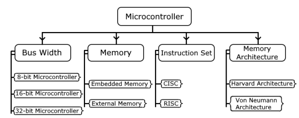
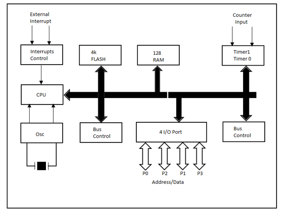
Figure 1. 8051 Architecture
Central Processor Unit (CPU)
The brain of any processing device of the microcontroller is the CPU. It monitors and controls all operations performed on these units. It reads program written in ROM memory, executes and does the expected task.
Interrupts
Interrupt is a subroutine call that interrupts the microcontrollers main operations or work and causes it to execute any other program, at the time of operation. It provides a mechanism to put on hold the ongoing operations, execute a subroutine and resume to another type of operation.
8051 has five interrupt sources:
INTO
TFO
INT1
TF1
R1/T1
(INT0) ̅ and (INT1) ̅ are external interrupts negative edge triggered or low level triggered. When these interrupts are activated, the corresponding flags are set except for serial interrupt.
When the processor branches to ISR the interrupt flags are cleared. The external interrupts are timer and serial port interrupts.
Memory
They require memory to save as well as read so that the microcontroller performs specific operations of the task.
The memory which is used to store the program known as code memory or Program memory It is also known as ROM memory.
8051 data memory is used to storing data temporarily for operation known as RAM memory. It has 4K of code memory or program memory and 128 bytes of data memory of RAM.
BUS
A collection of wires that work as communication channel or medium for transfer of data. It consists of 8, 16 or more wires of microcontroller. Thus, they carry 8 bits or 16 bits of data simultaneously. There are two types of buses which are
- Address Bus
- Data Bus
Address Bus:
Microcontroller 8051 has a 16-bit address bus for transferring data. It addresses memory locations to transfer address from CPU to Memory. It has four addressing modes that are:
- Immediate addressing modes.
- Bank address (or) Register addressing mode.
- Direct Addressing mode.
- Register indirect addressing mode.
Data Bus: Microcontroller 8051 has 8 bits of data bus used to carry data for applications.
Oscillator
The 8051 microcontroller has an on-chip oscillator that acts as a clock source for CPU of microcontroller. The output pulses of the oscillator are stable. Therefore, it enables synchronized work for all the parts of Microcontroller system.
Input/output Port
To control the operation of machines microcontroller is used in embedded systems. To connect to other machines, devices or peripherals I/O interfacing ports is required. Microcontroller 8051 has 4 input and output ports to connect to other peripherals
Timers/Counters
8051 microcontroller has two 16-bit timers and counters. The counters are again divided into 8-bit register. Timers are used for measurement of time intervals to determine pulse width.
Block Diagram
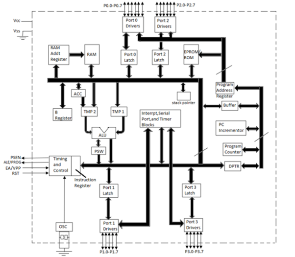
Figure 2. Block Diagram of 8051
1. ALU
ALU performs all arithmetic and logical functions.
Addition, subtraction with carry, and multiplication are categorized as arithmetic operations.
Logical AND, OR and exclusive OR (XOR) as logical operations.
2. Program Counter (PC)
A program counter is a 16-bit register that has no internal address. The program counter fetches the address of the next instruction to be executed from memory. The PC holds the address of next instruction residing in memory. When a command is encountered, it executes that instruction. PC increments and holds the address of the next instruction.
3. Registers
Registers are known as data storage devices. There are two registers namely Register A and Register B. Register A is used as an accumulator and Register B as general -purpose register. The output of mathematical and logical instructions are stored in these registers.
The operations of addition, subtraction, multiplication and division are performed by Register A. Register B is for multiplication and division which are carried by Register A. For data transfers between microcontroller and external memory Register A is involved.
8051 microcontrollers also have 7 Special Function Registers (SFRs). They are:
1. Serial Port Data Buffer (SBUF)
2. Timer/Counter Control (TCON)
3. Timer/Counter Mode Control (TMOD)
4. Serial Port Control (SCON)
5. Power Control (PCON)
6. Interrupt Priority (IP)
7. Interrupt Enable Control (IE)
4. Timers and Counters
In internal operations synchronization is achieved by clock circuits for generating clock pulses. During each clock pulse operations assure synchronization.
For oscillator formation XTAL1 and XTAL2 are used to form resonant network. It consists of four more pins.
1. EA: External enable
2. ALE: Address latch enable
3. PSEN: Program store enable and
4. RST: Reset.
Quartz crystal is used for generating periodic clock pulses.
5. Internal RAM and ROM
ROM
In 8051 a code of 4K memory is incorporated as on-chip ROM. ROM is a non-volatile memory that is its contents cannot be altered. They can address program memory and data memory which is a separate block of 64KB.
RAM
The internal RAM of 8051 microcontroller is composed of 128 bytes. It is a volatile memory because its contents are lost if power is switched off.
In internal RAM 128 bytes is divided into 32 working registers which constitute of 4 register banks (Bank 0-Bank 3), each bank consisting of 8 registers (R0 - R7). Internal RAM consists of 128 addressable bits.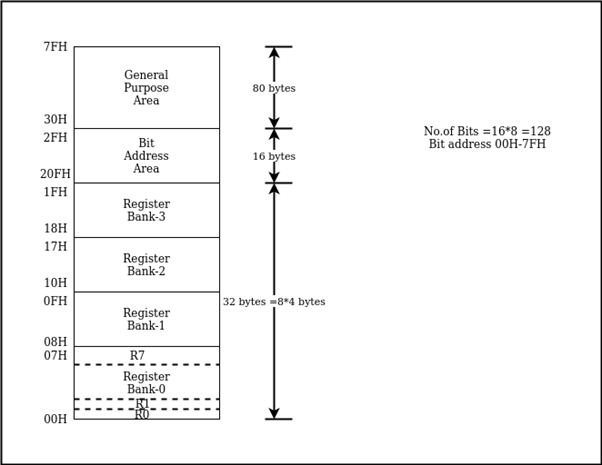
6. Four General Purpose Parallel Input/Output Ports
It consists of four 8-bit input/output ports. These are:
PORT P0: In absence of external memory present, this port acts as a general-purpose input/output port. In the presence of external memory, it operates as multiplexed address and data bus performing dual role.
PORT P1: This port is used for different interfacing activities. This 8-bit port is a normal I/O port and does not perform dual functions.
PORT P2: Port 2 is like PORT P0 which is used as general- purpose port if no external memory is present. However, in presence of external memory, it works in conjunction with PORT PO as an address bus. This is an 8-bit port which performs dual functions. PORT P3: PORT P3 behaves as dedicated I/O
port.
7. Interrupt Control
An interrupt is either an internal or external event where the microcontroller suspends for a certain time by obstructing the sequential flow of a program.
There are two ways of giving interrupts to a microcontroller
- Sending software instructions
- Sending hardware signals.
In interrupt mechanism 8051 keeps the normal program execution in “put on hold" mode and executes a subroutine program. After execution of subroutine, it returns to normal program execution. This subroutine program is called an interrupt handler. A subroutine is executed when certain event occurs.
8051 is provided with 5 sources of interrupts are provided. They are:
a) Two external interrupt sources connected through INT0 and INT1
b) Three external interrupt sources- serial port interrupt, Timer Flag 0 and Timer Flag 1.
8. Serial Data Communication
In serial data communication is established among computers by transmitting and receiving data bits in a serial connection network.
For holding data SBUF (Serial Port Data Buffer) register;
Manage data communication SCON (Serial Control) register
Managing data transfer rate PCON (Power Control) register
RXD and TXD establish serial network.
SBUF register has 2 parts
For storing the data to be transmitted use TXD pin
For receiving data from other source use RXD pin.
Serial data communication operates in four modes. They are serial data
1. Mode 0 (shift register mode)
2. Mode 1 (standard UART)
3. Mode 2 (multiprocessor mode)
4. Mode 3
9. PSW (Program Status Word)
Program Status Word or PSW is a hardware register a memory location which holds a program's information and monitors the status of the program this is currently being executed. It has a pointer which points towards the address of the next instruction to be executed.
The register has 3 fields namely instruction address field, condition code field and error status field. PSW is an internal register which keeps track of the computer at every instant.
There are7 flags in PSW. 4 are math flags and 3 are general purpose or user flags.
The Math flags are:
• Carry (c)
• Auxiliary carry (AC)
• Overflow (OV)
• Parity (P)
The General-purpose flags or User flags are:
• FO
• GFO
• GF 1
10. Data Pointer (DPTR)
DPTR is a 16-bit register. It consists of two 8-bit registers DPH and DPL. Separate addresses are assigned to each DPH and DPL. These 8-bit registers are used for storing memory addresses which can be accessed internal and external data/code.
11. Stack Pointer (SP)
A special area of data in memory. The stack pointer is an 8-bit register whose main function is to access the stack. It can take values in the range 00 H to FF H. SP acts as a pointer to points to an address at the top of the stack.
12. Data and Address Bus
A bus consists of group of wires to transfer data from one location to another within the system. Buses reduce the number of paths or cables needed to set up connection between components.
There are two kinds of buses - Data Bus and Address Bus
Data Bus: The purpose of data bus is to transfer data. It acts as a channel for data to travel.
Address Bus: The purpose of address bus is to transfer information but not data. The information tells from where within the components, the data should be sent to or received from.
Port Structure
8051 has four ports P0, P1, P2, P3. They are required for I/O operations.
32 pins are set for four ports P0, P1, P2, P3. Each port takes 8 pins.
All the ports are configured as input upon Reset
When zero is written to port it becomes output. To make it input 1 needs to be sent to the port.
Port 0:
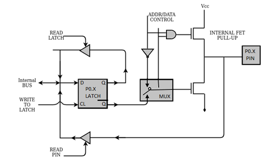
Fig 3. Port -0
When Port 0 is used as input port 1 must be written to the corresponding zero latch that causes the output transistor to switch off and pin floats in high impedance state.
When configured as input port it provides two facilities:
Reads logic level on physical pin by asserting read pin signal.
Read contents of internal latch by asserting the read latch signal.
The latch is read for instruction read-modify-write type instruction.
It reads data from the port modifies and writes to the port.
When Port0 is configured as output the latch pins that are programmed to 0 will cause the lower FET to turn ON and pin is grounded.
If 1 is written to the latch pin FET will turn OFF and pin is pulled HIGH by external pull-up resistor.
Port 1:
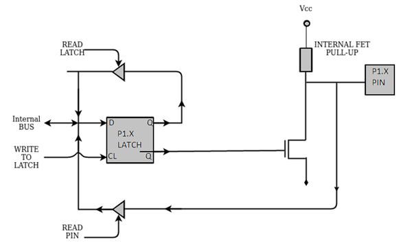
Figure 4. Port 1 circuit
When port 1 is used as in input port ‘1’ must be written to the corresponding port1 latch bit. This causes the lower FET to turn off.
The pin and the input buffer are pulled to logic HIGH by internal pull load.
This port is called quasi-bidirectional port because its output is pulled high with pull up resistor.
When port 1 is used as an output port, the latch pins that are programmed to 0, will cause the lower FET turn on the internal pull to turn off and input is logic 0.
If 1 is written onto the latch, then it will drive the input of external circuit high through pull up. The lower FET turns off.
Port 2:
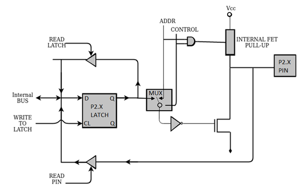
Figure 5. Port 2 circuit
When Port2 is used as an input port 1 must be written to the corresponding latch bit. This causes the FET turn off. The pin and input to pin buffer are pulled to logic high by internal pull up load.
Port 2 is called as “quasi-bidirectional port” as its output is pull up resistors.
When port2 is used as output port the latch pins that are programmed to 0, will cause the lower FET to turn off and input to the circuit logic 0.
If “1” is written onto latch pin, then it will drive the input of external circuit high through pull-up. The lower FET turns off.
Port 3:
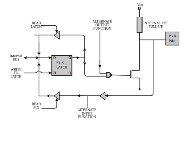
Figure 6. Port 3 circuit
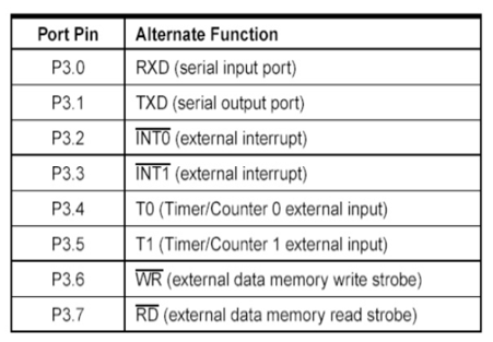
When port3 is used as input port 1 must be written to the corresponding port3 latch bit.
This causes FET to turn off.
The pin and input to the buffer are pulled to logic HIGH by internal pull up load.
When port3 is used as output port, the latched pins that are programmed to 0 will cause to lower FET to turn on and internal pull up to turn off and input to circuit is logic 0.
If 1 is written onto latch pin it will drive the input external circuit high through pull up. The lower FET turns off.
Key takeaway
- A special area of data in memory. The stack pointer is an 8-bit register whose main function is to access the stack. It can take values in the range 00 H to FF H. SP acts as a pointer to points to an address at the top of the stack.
- When Port0 is used as input port 1 must be written to the corresponding zero latch that causes the output transistor to switch off and pin floats in high impedance state.
It is an 8-bit register out of which only 6-bits are used by 88051 Microcontroller. The 2-bits which are not used are user definable flags. It has four flags which are affected as a result of some execution of any instruction. These flags are CY-carry, AC-auxiliary carry, P-Parity, OV-Overflow. The bit 3 and 4 of PSW are for register selection RS0 and RS1 and are also used to change bank register.
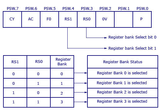
Fig 7 Program Status Word
The functions of above mentioned four flags are
CY (Carry Flag)
- When there is carry from D7 bit this flag is set.
- Usually, after arithmetic operations like addition and subtraction this flag is affected.
- With instructions like SET BC and CLRC this bit can be set to 1 or 0.
AC (Auxiliary Flag)
- This bit is set when a carry is generated from D3 to D4 during arithmetic operation. If not then it is clear.
- When instructions performing BCD arithmetic are executed this bit is used.
P (Parity Flag)
- The number of 1 in the accumulator are shown through this flag.
- When number of 1 in accumulator are 1, P=1 and P=0 when number of 1 in accumulator is even.
OV (Overflow Flag)
- When result of signed number operation is large this flag is set. Because of which higher order bit overflow into the sign bit.
- To detect error in signed arithmetic operations this flag is used.
Key takeaway
It is an 8-bit register out of which only 6-bits are used by 88051 Microcontroller. It has four flags which are affected as a result of some execution of any instruction. These flags are CY-carry, AC-auxiliary carry, P-Parity, OV-Overflow.
Data Transfer Instructions
The Data Transfer Instructions relate to transfer of data between registers or external program memory or data memory. The Mnemonics associated with Data Transfer are given below.
- MOV
- MOVC
- MOVX
- PUSH
- POP
- XCH
- XCHD
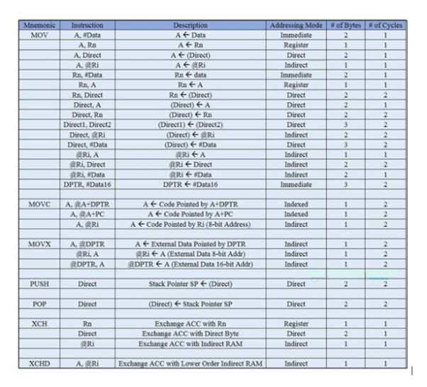
Arithmetic Instructions
Using Arithmetic Instructions, one can perform addition, subtraction, multiplication and division. It consists of increment by one, decrement by one and a special instruction called Decimal Adjust Accumulator.
The Mnemonics associated with the Arithmetic Instructions of the 8051 Microcontroller Instruction Set are:
- ADD
- ADDC
- SUBB
- INC
- DEC
- MUL
- DIV
- DA A
The arithmetic instructions have no knowledge about the data format that is signed, unsigned, ASCII, BCD, and so on. The operations performed by the arithmetic instructions affect flags like carry, overflow, zero, etc. in PSW Register.
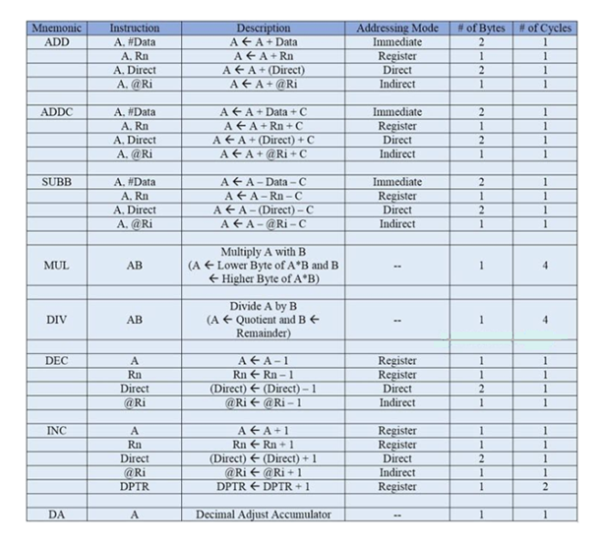
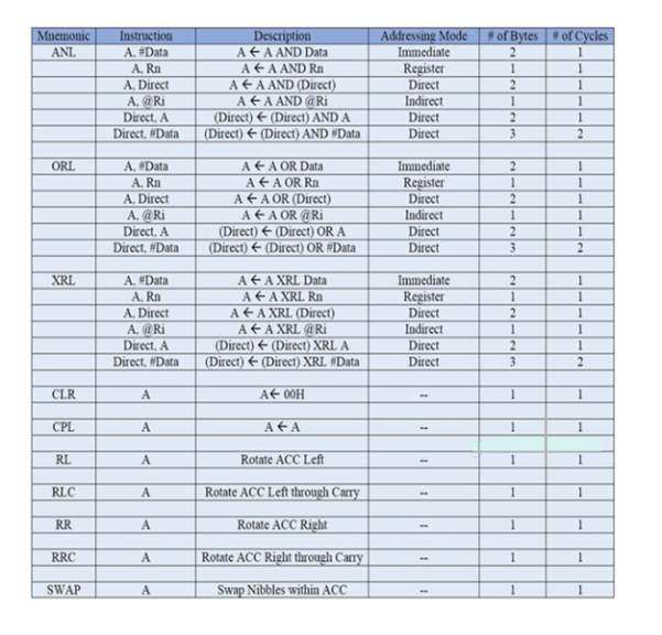
Logical Instructions
Logical Instructions perform logical operations like AND, OR, XOR, NOT, Rotate, Clear and Swap. Logical Instruction are performed on bytes of data on a bit-by-bit basis.
Mnemonics associated with Logical Instructions are as follows:
- ANL
- ORL
- XRL
- CLR
- CPL
- RL
- RLC
- RR
- RRC
- SWAP
Bit Manipulation Instructions
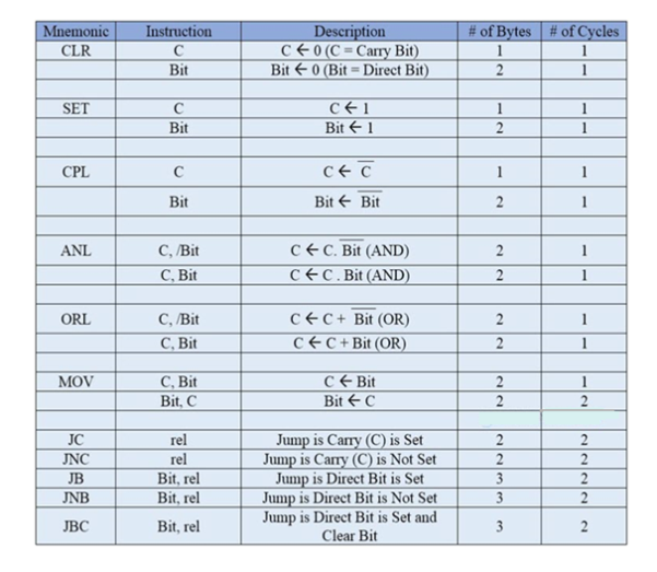
Boolean or Bit Manipulation Instructions will deal with bit variables. There is a special bit-addressable area in RAM and some Special Function Registers (SFRs) that are bit addressable.
The Mnemonics corresponding to the Boolean or Bit Manipulation instructions are:
- CLR
- SETB
- MOV
- JC
- JNC
- JB
- JNB
- JBC
- ANL
- ORL
- CPL
These instructions perform set, clear, and, or, complement at bit level. All the possible mnemonics of the Boolean Instructions are specified in the following table.
Program Branching Instructions
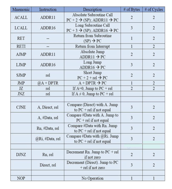
The logic of the program is controlled by these instructions. The mnemonics of the Program Branching Instructions are:
- LJMP
- AJMP
- SJMP
- JZ
- JNZ
- CJNE
- DJNZ
- NOP
- LCALL
- ACALL
- RET
- RETI
- JMP
All these instructions, except the NOP (No Operation) affect the Program Counter (PC) Some of these instructions have decision making capability before transferring control to other part of the program.
The following table shows all the mnemonics with respect to the program branching instructions.
Key takeaway
There are following group of instructions:
- Arithmetic Instructions.
- Data transfer Instructions.
- Bit Manipulation.
- Program Branching Instructions.
- Logical Instructions.
The 8051 Microcontroller Memory is separated into Program Memory (ROM) and Data Memory (RAM). The Program Memory of the 8051 Microcontroller is used for storing the program to be executed, which means instructions. The Data Memory is used for storing temporary variable data and intermediate results.
Program Memory (ROM) of 8051
The code or instructions which are to be executed are stored in the Program Memory, also called as the ROM of the Microcontroller.
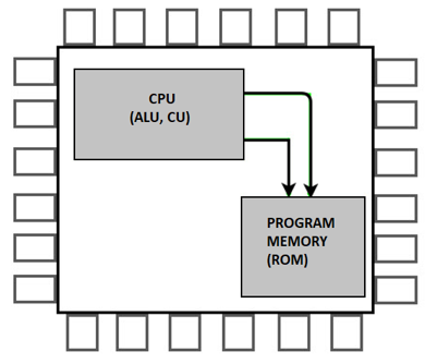
Figure 8. Program Memory
In 4KB Internal ROM, the address space is 0000H to 0FFFH. If the program addresses exceed this value, CPU will automatically fetch the code from the external Program Memory.
For External Access (EA Pin) must be pulled HIGH at this condition the CPU first fetches instructions from the Internal Program Memory in the address range of 0000H to 0FFFFH. If it exceeds the memory addresses limit, instructions are fetched from external ROM in address range of 1000H to FFFFH.
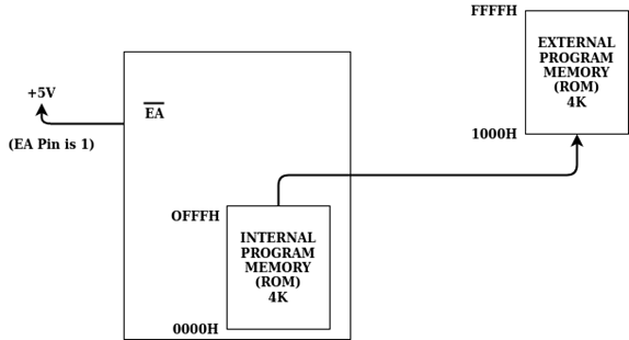
Figure 9. External access
There is also an alternative method to fetch the instructions where the Internal ROM is ignored and instructions are fetched only from External Program Memory (External ROM).
For this purpose, EA pin must be connected to GND. The memory addresses of external ROM will be from 0000H to FFFFH.
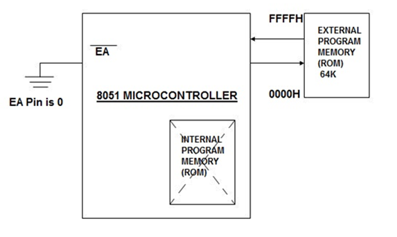
Figure 10. External Program Memory
Data Memory (RAM)
Data Memory or RAM stores temporary data and intermediate results generated during the normal operation of the microcontroller.
Currently, 8051 Microcontroller has 256B of RAM. The first 128B memory addresses from 00H to 7FH is divided in to Working Registers. They are organized as Register Banks, Bit – Addressable Area and General-Purpose RAM known as Scratchpad area.
The first 128B of RAM (from 00H to 7FH), the first 32B of memory from addresses 00H to 1FH consists of 32 Working Registers organized into four banks with 8 Registers in each Bank.
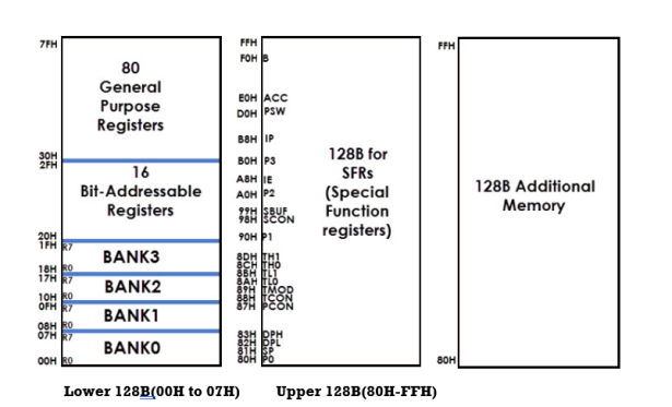
Fig 11 (Direct and Indirect Addressing) (Direct Addressing) (Indirect Addressing)
The 4 banks are named as Bank0, Bank1, Bank2 and Bank3. Each Bank consists of 8 registers R0 – R7. Each Register can be addressed either by name or by address.
To address the register by name, first the corresponding bank is selected. In order to select the bank, RS0 and RS1 bits of the Program Status Word (PSW) and Register (RS0 and RS1 are 3rd and 4th bits in the PSW Register) are used.
When addressing these Register for example 12H the corresponding bank may or may not be selected. (12H corresponds to R2 in Bank2).
The next 16B of the RAM that is from 20H to 2FH are Bit – Addressable memory locations. A total of 128 bits can be addressed individually using 00H to 7FH or an entire byte can be addressed as 20H to 2FH.
The final 80B of the internal RAM addresses are from 30H to 7FH which is the general-purpose RAM area are byte addressable.
These lower 128B of RAM can be addressed directly or indirectly.
Key takeaway
- For External Access (EA Pin) must be pulled HIGH at this condition the CPU first fetches instructions from the Internal Program Memory in the address range of 0000H to 0FFFFH. If it exceeds the memory addresses limit, instructions are fetched from external ROM in address range of 1000H to FFFFH.
- Currently, 8051 Microcontroller has 256B of RAM. The first 128B memory addresses from 00H to 7FH is divided in to Working Registers.
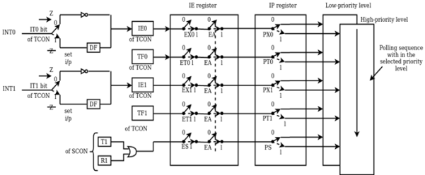
Figure 12. Interrupt Structure of 8051
8051 has five interrupts. These are INT0, INT1, T0, T1, TI/RI. All these interrupts can be enabled or disabled by IE (interrupt enable) register.
Interrupt Enable (IE)Register
This register can be used to enable or disable interrupts by programming. It is an SFR with address A8H. This byte is bit addressable hence can be programmed by the user. Every bit in this register has a specific meaning.


Interrupt Priority (IP) Register
The five interrupts can be either one or two interrupt level. The priority levels are level 1 and level 0. Higher Priority is indicated by level 1 and level 0 indicates lower priority. To store priority levels for each interrupt IP register is used. This is bit addressable SFR with address B8H.


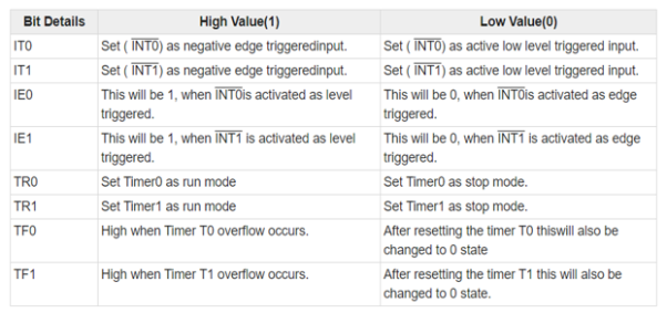
External Interrupt
The external interrupts are INT0 and INT1. The TCON register can be used to program external interrupts to edge or level triggered. The TCON is Timer Control. TCON is another bit addressable SFR. The address is 88H.
Key takeaway
Interrupt is a subroutine call that interrupts the microcontroller's main operations or work and causes it to execute any other program, at the time of operation. It provides a mechanism to put on hold the ongoing operations, execute a subroutine and resume to another type of operation.
8051 has five interrupts as mentioned below:
- INTO
- TFO
- INT1
- TF1
- R1/T1
The interrupts (INT0) ̅ and (INT1) ̅ are called as external interrupts. The interrupts (INT0) ̅ and (INT1) ̅ are negative edge triggered. When, these interrupts are activated, the corresponding flags are set except for serial interrupts.
There are two 16-bit timer registers are known as Timer0 and Timer1. The timer registers are used as Timer mode and Counter mode. The only difference in these two modes is the source for incrementing the timer registers.
Timer Mode
In timer mode, it counts internal machine cycles. So, this register gets incremented for each machine cycle. When the clock frequency is 12MHz, timer register is incremented for every millisecond. It ignores external timer input pin in this mode.
Counter Mode
In counter mode, it counts external events. The timer register gets incremented for every 1 to 0 transition in the external input pin. This type of transitions is referred as events.
The external input pins are sampled once for each machine cycle. In order to determine 1or 0 transitions another machine cycle is required.
Therefore, atleast two machine cycles are required in this mode. When frequency is12MHz the maximum count frequency will be 12MHz/24 = 500KHz. So, for event counting time duration is 2 µs.
Timer or Counter has four different modes. Mode 0 to Mode 2 are for both Timer/Counter. Mode 3 represent different meaning for each timer register. There is a register called TMOD which can be programmed to configure these timers or counters.
The Serial port is used for serial communication in mode 1 and 3. For baud rate generation timer1 is used. Hence, Timer0 is available for timer or counter operations.
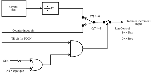
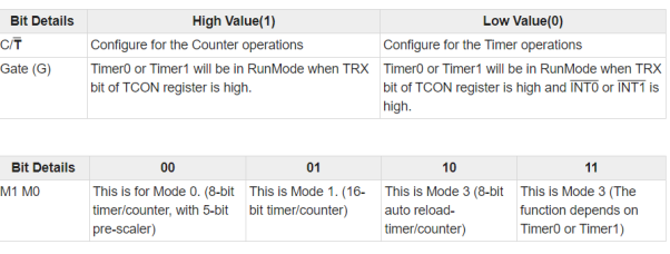
TMOD Register
TMOD (Timer Mode) is an SFR. The address of this register is 89H. This is not bit-addressable.

Mode 0 of Timer/Counter
Mode 0 operation is 8-bit timer or counter with 5-bit pre-scaler. It is 13-bit timer/counter. Which uses 5 bits of TL0 or TL1 and 8-bits of TH0 or TH1.

Figure 13. Mode 0
Mode 1 of Timer/Counter
Mode 1 operation is 16-bit timer or counter. In the following diagram, Mode 1 is used for Timer0.

Figure 14. Mode 1
Mode 2 of Timer/Counter
Mode 2 operation is 8-bit auto reload timer or counter. Mode 2 is used for Timer1.
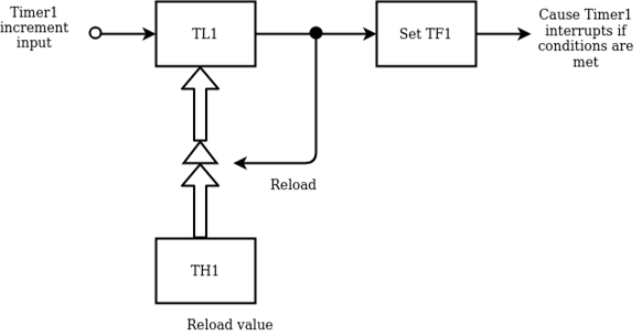
Figure 15. Mode 2
Mode 3 of Timer/Counter
Mode 3 is different for Timer0 and Timer1. When Timer0 is working in mode 3, TL0 will be used as 8-bit timer/counter. It will be controlled by standard Timer0 control bits, T0 and INT0 inputs. TH0 is used as 8-bit timer not counter. This is controlled by Timer1 Control bit TR1. When the TH0 overflows from FFH to 00H, TF1 is set to 1. In the following diagram, Timer0 is in Mode 3.

Figure 16. Mode 3
Operation:
- It controls the running of 8-bit timer/counter TL0 like Mode 0, 1, or 2. The running of TH0 is controlled by TR1 bit. So, the gate bit in this mode for Timer0 has no specific role.
- The mode 3 is present for applications requiring an extra 8-bit timer/counter. In Mode 3 of Timer0, 8051 has three timers. One 8-bit timer by TH0, another8-bit timer/counter by TL0, and one 16-bit timer/counter by Timer1.
- If Timer0 is in mode3, and Timer1 is working on either 0, 1 or 2, then the gun control of the Timer1 is activated when the gate bit is low or INT1 is high. The run control is deactivated when the gate is high and INT1 is low.
Key takeaway
- Timer or Counter has four different modes. Mode 0 to Mode 2 is for both Timer/Counter. Mode 3 represent different meaning for each timer register. There is a register called TMOD which can be programmed to configure these timers or counters.
- The Serial port is used for serial communication in mode 1 and 3. For baud rate generation timer1 is used. Hence, Timer0 is available for timer or counter operations.
It is also called the Universal Asynchronous Receiver Transmitter used in serial communication. It basically does serial to parallel data conversion on the transmitter side. Again, at the receiver side it converts the received data from serial to parallel. It is an interconnection between the processor and the serial communication port.

Figure 17 UART
Above figure shows the connection of UART with the controller and USB interface. The timing settings between the transmitter and receiver in this case are of major concern. To maintain synchronisation UART uses special bits at the starting and end of each word.
The UART at the sender end receives the parallel data and converts it to serial data. The receiving side UART receives this serial data and converts it to parallel and sends it back to the CPU.
Working of UART
The transmission in UART is asynchronous. The transmitter and receiver do not have any timing synchronisation. There are special bits which are used for synchronisation. They are called Start and Stop bits.
These bits are attached at the start and end of the data allowing the receiver to identify the actual data. The data bus transfers the data to the transmitting UART from the controlling device. This received data is in parallel.
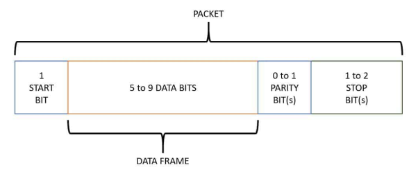
The start, parity and stop bits are added to this received data. After inserting the special bits, they are converted to serial data with the help of shift registers. At the Rx pin the receiving UART receives this serial data. The original data is recognised by the special bits. Parity bit is used to check the integrity of the data.
The special bits are separated from the received data and it is again converted back to parallel data. Through the data bus this data is sent back to the receiving end of the controller.
Necessary requirement for UART
The requirements for data transmission are mentioned below.
- Synchronisation Bits (Start and Stop bits)
- Parity Bit
- Data Bits and
- Baud Rate
The rate of data transmission is called Baud rate. It is measured in bits per second.
Calculation of Baud Rate
In order to calculate the machine cycle frequency, the 8051 divides the crystal frequency by 12. The oscillator frequency is 11.0592 MHz.

Figure 18 Oscillator Frequency
Here the oscillator is XTAL = 11.0592 MHz, the machine cycle frequency is 921.6 kHz. 8051's UART divides the machine cycle frequency of 921.6 kHz by 32 once more before it is used by Timer 1 to set the baud rate. 921.6 kHz divided by 32 gives 28,800 Hz. Timer 1 must be programmed in mode 2, that is 8-bit, auto-reload.
Example
In serial communication if data transferred with a baud rate of 9600 and XTAL used is 11.0592 then following is the steps followed to find the TH1 value to be loaded.
Clock frequency of timer clock: f = (11.0592 MHz / 12)/32 = 28,800Hz
Time period of each clock tick: T0 = 1/f = 1/28800
Duration of timer: n*T0 (n is the number of clock ticks)
9600 baud ->duration of 1 symbol: 1/9600
1/9600 = n*T0 = n*1/28800
n = f/9600 = 28800/9600 = 3 ->TH1 =-3
Similarly, for baud 2400 n = f/2400 = 12 ->TH1 = -12
In 8051 data transfers and reception operate serially at different baud rates. Serial communications are established with PC through the COM port for interface. The baud rate in 8051 is programmable with the help of timer. When used as serial port, the frequency of timer tick is determined by (XTAL/12)/32 and 1 bit is transmitted for each timer period.
The relationship between the crystal frequency and baud rate is that 8051divides the crystal frequency by 12 to get the machine cycle frequency as shown in figure.
Here the oscillator is XTAL = 11.0592 MHz, the machine cycle frequency is 921.6 kHz.
8051's UART divides the machine cycle frequency by 921.6 kHz by 32 once before it is used by Timer 1 to set the baud rate. When 921.6 kHz is divided by 32 it gives 28,800 Hz. Therefore, Timer 1 must be programmed in mode 2 which means 8-bit auto-reload.
Registers for serial communication
SBUF (serial buffer) register:
It is an 8- bit register used for serial communication. A byte of data is transferred via TxD line placed in SBUF register. SBUF holds this byte of data when received by RxD line. It can be accessed by any other register.
MOV SBUF, #'D'; load SBUF=44H, ASCII for 'D„
MOV SBUF, A; copy accumulator into SBUF
MOV A, SBUF; copy SBUF into accumulator
When a byte of data is written, it is framed with start and stop bits and transferred serially via the TxD pin and received serially via RxD and deframed by eliminating the stop and start bits making a byte out of the data received, and placed in SBUF.
SCON Register

The first two bits are SM0, SM1 which represent serial port mode bits. It is used to specify framing format for baud rate calculation.
For example, if (SM0, SM1) = (0,1), mode 1: 8-bit data, 1 start bit, 1 stop bit, variable baud rate can be set by timer.
The other three modes are rarely used and they are (SM0, SM1) = (0,0), mode 0: fixed baud = XTAL/12, (SM0, SM1) = (1,0), mode 2: 9-bit data, fixed baud, (SM0, SM1) = (1, 1), mode 3: 9-bit data, variable baud.
The third bit is used to select processor type used for communication.
If SM2 = 0 single processor communication.
If SM2 = 1, multiprocessor communication.
The fourth bit REN is Receive Enable used to enable/disable reception.
If REN=1, 8051 will accept incoming data from serial port.
If REN=0, receiver is disabled.
E.g., SETB REN, CLR REN, SETB SCON.4, CLR SCON.4.
The fifth bit is TB8 used by modes 2 and 3 for 8-bit transmission.
When mode = 1 pin TB8 should be cleared.
The sixth bit RB8 is used by modes 2 and 3 for the reception of 8th bit. To store the stop bit mode 1 is used.
The seventh bit is TI is Transmit Interrupt. After completion of transfer of 8-th bit character it sets TI to ''1'' to indicate that it is ready to transfer the next character. The TI is raised at the beginning of stop bit.
The last bit is RI which is the receive interrupt. When 8051 receives a character, the UART removes start bit and stop bit and puts the 8-bit character in SBUF.
RI is set to 1 to indicate that a new byte is ready to be picked up in SBUF. It is raised halfway through the stop bit.
Steps to send data serially:
1.Set baud rate by loading TMOD register with value 20H, indicating timer-1 in mode 2 (8-bit auto-reload) and set baud rate.
2. TH1 is loaded with values to set baud rate for serial data transfer.
3. The SCON register is loaded with 50H, indicating serial mode 1, where an 8- bit data is framed with start and stop bits.
4. TR1 is set to 1 in order to start timer 1.
5. By CLR TI instruction TI is cleared
6. For character byte to be transferred serially it is written into SBUF register.
7. In order to check if the character is transferred completely, the TI flag bit is monitored by JNB TI instruction.
8. Jump to step 5 for transfer of next byte.
Program to transfer letter “D” serially at 9800baud, continuously:
MOV TMOD, #20H; timer 1, mode 2(auto reload)
MOV TH1, #-3; 9600 baud rate
MOV SCON, #50H; 8-bit, 1 stop, REN enabled
SETB TR1; start timer 1
AGAIN: MOV SBUF, #”D; letter “D” to transfer
HERE: JNB TI, HERE; wait for the last bit
CLR TI; clear TI for next char
SJMP AGAIN; keep sending A
Steps to receive data serially:
1. Set baud rate by loading TMOD register with value 20H, to indicates that timer 1 is in mode2 (8-bit auto-reload) and set baud rate
2. TH1 is loaded with value to set baud rate.
3. The SCON register is loaded with value 50H, indicating serial mode 1, where an 8- bit data is framed with start and stop bits.
4. TR1 is set to 1 to start timer 1.
5. RI is cleared by CLR RI instruction
6. The RI flag bit is monitored by JNB RI instruction to see if an entire character has been received.
7. When RI is raised, SBUF has a byte, its contents are moved into to safe place.
8. To receive next character, jump to step 5
Program to receive bytes of data serially, and put them in P2, set the baud rate at 9600, 8-bit data, and 1stop bit:
MOV TMOD, #20H; timer 1, mode 2(auto reload)
MOV TH1, #-3; 9600 baud rate
MOV SCON, #50H; 8-bit, 1 stop, REN enabled
SETB TR1 start timer 1
HERE: JNB RI, HERE; wait for char to come in
MOV A, SBUF; saving incoming byte in A
MOV P2, A; send to port 1
CLR RI; get ready to receive next byte
SJMP HERE; keep getting data
Exchange the content of FFH and FF00H
MOV dptr, #0FF00H; take the address in dptr
MOVX A, @dptr; get the content of 0050H in a
MOV r0, 0FFH; save the content of 50H in r0
MOV 0FFH, a; move a to 50H
MOV A, r0; get content of 50H in a
MOVX @dptr, a; move it to 0050H
Store the higher nibble of r7 in to both nibbles of r6
Firstly, we get the upper nibble of r7 in r6. Then we swap nibbles of r7 and make OR operation with r6 so the upper and lower nibbles are duplicated
MOV A, r7; get the content in acc
ANI A, #0F0h; mask lower bit
MOV r6, A; send it to r6
SWAP A; exchange upper and lower nibbles of accumulator
ORL A, r6; OR operation
MOV r6, A; finally load content in r6
Transfer the block of data from 20H to 30H to external location 1020H to 1030H.
MOV r7, #0AH; initialize counter by 10d
MOV r0, #20H; get initial source location
Mov dptr, #1020H; get initial destination location
Nxt: MOV A, @r0; get first content in acc
MOVX @dptr, a; move it to external location
INC r0; increment source location
INC dptr; increase destination location
DJNZ r7, nxt; decrease r7. If zero then over otherwise move next
Given block of 100h to 200h. Find out how many bytes from this block are greater then, the number in r2 and less then number in r3. Store the count in r4.
MOV dptr, #0100H ; get initial location
MOV r7, #0FFH ; counter
MOV r4, #00H ; number counter
MOV 20H, R2 ; get the upper and lower limits in
MOV 21H, R3 ; 20H and 21H
Nxt: MOVX A, @dptr ; get the content in acc
CJNE A, 21H, lower ; check the upper limit first
SJMP out ; if number is larger
Lower: JNC out ; jump out
CJNE A, 20H, limit ; check lower limit
SJMP out ; if number is lower
Limit: JC out ; jump out
INC r4 ; if number within limit increment count
Out: INC dptr ; get next location
DJNZ r7, nxt ; repeat until block completes
Find out how many equal bytes between two memory blocks 10H to 20H and 20H to 30H.
MOV r7, #0AH ; initialize counter by 10d
MOV r0, #10H ; get initial location of block1
MOV r1, #20H ; get initial location of block2
MOV r6, #00H ; equal byte counter. Starts from zero
Nxt: MOV A, @r0 ; get content of block 1 in acc
MOV b, a ; move it to B
MOV A, @r1 ; get content of block 2 in acc
CJNE A, B, nomatch ; compare both if equal
INC r6 ; increment the counter
Nomatch: INC r0 ; otherwise go for second number
INC r1
DJNZ r7, nxt ; decrease r7. If zero then over otherwise move next
Delay using Timer.
- Assume the processor is clocked by 12MHz crystal.
- That means, the timer clock input will be 12MHz/12 = 1MHz
- That means, the time taken for the timer to make one increment = 1/1MHz = 1uS
- For a time, delay of “X” uS the timer has to make “X” increments.
- 2^16 = 65536 is the maximum number of counts possible for a 16-bit timer.
- Let TH be the value loaded to TH registered and TL be the value loaded to TL register.
- Then, THTL = Hexadecimal equivalent of (65536-X) where (65536-X) is considered in decimal.
Let the required delay be 1000uS (i.e.; 1mS).
That means X = 1000
65536 – X = 65536 – 1000 = 64536.
64536 is considered in decimal and converting it t0 hexadecimal gives FC18
That means THTL = FC18
Therefore TH=FC and TL=18
The program can be used for generating 1mS delay
DELAY: MOV TMOD, #00000001B // Sets Timer 0 to MODE1 (16-bit timer). Timer 1 is not used
MOV TH0, #0FCH // Loads TH0 register with FCH
MOV TL0, #018H // Loads TL0 register with 18H
SETB TR0 // Starts the Timer 0
HERE: JNB TF0, HERE // Loops here until TF0 is set (i.e., until roll over)
CLR TR0 // Stops Timer 0
CLR TF0 // Clears TF0 flag
RET
Delay using interrupt
Begin:
Mov i.e., #0; turn off all interrupts
Mov sp, #stack-1
Mov hours, #0; zero hours, minutes, seconds
Mov minutes, #0
Mov seconds, #0
Mov ov_countdown, #225
Clr tr0; make sure timer 0 is stopped
Clr tf0; clear the overflow flag
Anl tmod, #0xF0; set to mode 0 (without touching timer 1)
Mov th0, #0; clear the timer 0 value
Mov tl0, #0
Mov dptr, #msg_begin
Lcall pstr
Clr time_changed_flag
Setb tr0; start the timing
Mov ip, #0; set interrupt priorities (all low)
Mov ie, #0x82; enable timer0 interrupt
Lcall print_time
Timekeeping_loop:
Lcall esc
Jc abort
Jnb time_changed_flag, timekeeping_loop
Clr time_changed_flag
Lcall print_time
Sjmp timekeeping_loop
;this interrupt service routine will run every time timer0 sets
;the TF0 flag. The 8051 hardware automatically clears TF0 for
;us. As with all interrupts, we must be very careful to save
;any registers that get changed.
Timer0_isr:
Djnz ov_countdown, timer0_end; have 225 interrupts (1 second) elapsed?
Mov ov_countdown, #225
Push psw; save psw (cjne changes status bits)
Push acc; save accumulator, used inside inc_time
Acall inc_time; actually, increment the time
Setb time_changed_flag; set a flag to alert the main program to change
Pop acc
Pop psw
Timer0_end:
Reti
Write a test program for the DS89C420/30 chip to toggle all the bits of PO, PI, and P2 every 1/4 of a second. Assume a crystal frequency of 11.0592 MHz.
ORG 0
BACK: MOV A, #55H
MOV P0, A
MOV P1, A
MOV P2, A
ACALL QSDELAY
SJUMP BACK
QSDELAY:
MOV R5, #11
H3: MOV R4, #248
H2: MOV R3, #255
H1: DJNZ R3, H1
DJNZ R4, H2,
DJUNZ R5, H3
Delay = 11 x 248 x 255 x 4MC x 90ns = 250,430 s
s
Create a square wave of 50% duty cycle on bit 0 of port 1.
The 50% duty cycle means that the "on" and "off' states (or the high and low
Portions of the pulse) have the same length. Therefore, we toggle Pl.0 with a
Time delay in between each state.
HERE: SETB P1.0
LCALL
CLR PI. 0
LCALL DELAY
SJMP HERE
Another way to write the above program is:
HERE: CPL P1.0
LCALL DELAY
SJMP HERE
Create a square wave of 66% duty cycle on bit 3 of port 1
BACK: SETB Pl.3
LCALL DELAY
LCALL DELAY
CLR P1.3
LCALL DELAY
SJMP BACK
Write a program to perform the following:
(a) keep monitoring the Pl.2 bit until it becomes high
(b) when P 1.2 becomes high, write value 45H to port 0
(c) send a high-to-Iow (H-to-L) pulse to P2,3
SETB PI.2
MOV A, #45H
AGAIN JNB PI.2, AGAIN
MOV PO, A
SETB P2.3
CLR P2.3
In this program, instruction "JNB PI 2 AGAING” (JNB means Jump if no bit) stays in the loop as long as P 1.2 is low. When P.12 becomes high. It gets out of the loop. Writes the value 45H to port 0 and creates an H-to-L pulse by the sequence of instruction SETB and CLR.
Assume that bit P2.3 is an input and represents the condition of an oven. If it goes high, it means that the oven is hot. Monitor the bit continuously. Whenever it goes high, send a high-to-low pulse to port P 1.5 to tum on a buzzer.
HERE: JNB P2.3, HERE
SETB Pl. 5
CLR Pl. 5
SJMP HERE
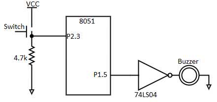
A switch is connected to pin P 1.7. Write a program to check the status of SW and perform
The following:
(a) If SW=O, send letter 'N' to P2.
(b) If SW=I, send letter 'Y'toP2.
SETB Pl.?
AGAIN JB Pl.2, OVER
MOV P2, #'N'
SJMP AGAIN
OVER MOV P2, #'Y'
SJMP AGAIN
A switch is connected to pin PI. 7. Write a program to check the status of the switch and
Perform the following:
(a) If switch = 0, send letter 'N' to P2.
(b) If switch = I, send letter 'Y'toP2.
SET P1.7
AGAIN: MOV C, P1.2
JC OVER
OVER: MOV P2, #’N’
SJMP AGAIN
A switch is connected to pin P1.0 and an LED to pin P2.7 status of the switch and send it to the LED
SET P1.7
AGAIN: MOV C, P1.0
MOV P2.7, C
SJMP AGAIN
Write 8051 C program to toggle all the bits of port P I continuously with some delay in between. Use Timer 0, 16-bit mode to generate the delay.
#include <reg5I.h>
Void TODelay(void);
Void main (void)
{
While(l) //repeat forever
{
Pl=Ox55; //toggle all bits of PI
T0Delay (); //delay size unknown
Pl=OxAA; //toggle all bits of PI
T0Delay ();
}
}
Void T0 Delay ()
{
TMOD=0x01; //Timer 0, Mode 1
TL0=0x00; //load TL0
TH0=0x35; //load TH0
TR0=l; //turn on T0
While (TF0==0); //wait for TF0 to rollover
TR0=0; //turn off T0
TF0=0; //clear TF0
}
FFFFH - 3500H = CAFFH = 51967 + 1 = 51968
51968 x 1.085  s = 56.384 ms is the approximate delay
Write an 8051 C program to toggle only bit P 1.5 continuously every 50 ms. Use Timer 0, mode I (l6-bit) to create the delay. Test the program (a) on the AT89C51 and (b) on the DS89C420.
#include <regsl.h>
Void T0M1Delay(void);
Sbit mybit=PIAS;
Void main (void)
{
While(l)
{
Mybit=-mybit; //toggle Pl.5
T0MIDelay (); //Timer 0, mode 1(16-bit)
}
}
(a) Tested for AT89C51, XTAL=II.0592 MHz,
Void T0M1Delay(void)
{
TMOD=0x0l; //Timer 0, mode 1(16-bit)
TL0=0xFD; //load TL0
TH0=0x4B;//load TH0
TR0=l; //turn on T0
While (TF0==0); //wait for TF0 to rollover
TR0=0; //turn off T0
TF0=0; //clear TF0
}
(b) Tested for D589C420, XTAL=II.0592 MHz,
Void T0M1Delay(void)
{
TMOD=0x0l; //Timer 0, mode 1(16-bit)
TL0=0xFD; //load TL0
TH0=0x4B; //load TH0
TR0=l; //turn on T0
While (TF0==0); //wait for TFO to rollover
TR0=0; //turn off T0
TF0=0; //clear TF0
}
FFFFH - 4BFDH = B402H = 46082 + 1 =46083
Timer delay = 46083 x 1.085  s = 50 mS
Write an 8051 C program to toggle a11bits of P2 continuously every 500 ms.
Timer 1, mode 1 to create the delay.
#include <regsl.h>
Void TIMIDelay(void);
Void main (void)
Unsigned
P2=OxSS;
While (1);
{
P2=-P2; //toggle all bits of P2
For(x=O;x<20;x++)
TIMlDelay();
}
}
Void TIMIDelay(void)
TMOD=0xl0; //Timer 1, mode 1(16-bit)
TLl=0xFE; //load TLI
THl=0xAS; //load THI
TRl=l; //turn on Tl
While (TFl==0); //wait for TFI to rollover
TRl=0; //turn off Tl
TFl=0; //clear TFI
}
A5FEH = 42494 in decimal
65536 - 42494 = 23042
23042 x 1.085  s = 25 ms and 20 x 25 ms = 500 ms
Write an 8051 C program to toggle only pin P1.5 continuously every 250 ms. Use Timer 0, mode 2 (8-bit auto-reload) to create the delay
#include <reg51.h>
Void T0M2Delay(void);
Sbit mybit=PIA5;
Void main (void)
{
Unsigned char x, y;
While (1)
{
Mybit=-mybit; //toggle Pl. 5
For(x=O,x<250;x++) //due to for loop overhead
For(y=O;y<36;y++) //we put 36 and not 40
T0M2Delay();
}
}
Void T0M2Delay(void)
{
TMOD=0x02; //Timer 0, mode 2(B-bit auto-reload)
TH0=-23; //load TH0 (auto-reload value)
TR0=I; //turn on T0
While (TF0==0); //wait for TFO to rollover
TR0=0; / / turn off. T0
TF0=0; //clear TF0
}
256 - 23 = 233
23 x 1.085  s = 25
  s
s
25  s x 250 x 40 = 250 ms by calculation.
Write an 8051 C program to create a frequency of 2500 Hz on pin P2. 7. Mode 2 to create the delay.
#include <regS1.h>
Void T1M2Delay(void);
Sbit mybit=P2.7;
Void main (void)
(
Unsigned char X;
While (1)
(
Mybit=-mybit;
TlM2Delay ();
}
}
Void T1M2Delay(void)
TMOD=0x20; //Timer 1, mode 2(8-bit auto-reload)
TH1=-184; //load TH1(auto-reload value)
TR1=1;//turn on T1
While (TF1==0); //wait for TF1 to roll over
TR1=0; //turn off T1
TF1=0;//clear TF1
}
1 / 2500 Hz = 400  s
s
400  s / 2 = 200
  s
s
200  s / 1.085
  s =184
A switch is connected to pin P 1.2. Write an 8051 C program to monitor SW and create the following frequencies on pin PI.7:
SW=O: 500 Hz
SW=l: 750Hz
Use Timer 0, mode 1 for both of them.
#include <reg51.h>
Sbit mybit=P1^5;
Sbit SW=P1^7;
Void TOMIDelay(unsiged char);
Void main (void)
{
SW=l, //make PI.7 an input
While (1)
{
Mybit=-mybit;
If (SW==0)
TOMlDelay (0);
Else
T0MlDelay (1);
}
}
Void TOMIDelay(unsigned char c)
{
TMOD=0X01;
If (c==0)
{
TL0=0x67; //FC67
TH0=0xFC;
}
Else
{
TL0=0x9A; //FD9A
TH0=0xFD;
}
TRO=l;
While (TF0==0);
TR0=0;
TF0=0,
}
FC67H = 64615
65536 - 64615 = 921
921 X 1.085  s = 999.285
  s
s
1 / (999.285  s X 2) = 500 Hz
Assume that a l-Hz external clock is being fed into pin T1 (P3.5). Write a C program for counter I in mode 2 (8-blt auto reload) to count up and display the state of the TLI count on P I. Start the count at 0H.
#include <regSI.h>
Sbit Tl = P3'S;
Void main (void)
{
T1=1; //make T1 an input
TMOD=0X60;
TH1=0; //set count to 0
While (1)
{
Do //repeat forever
{
TR1=1; //start timer
PhTL1; //place value on pins
}
While (TF1==O)
TR1=0;
TFl=0;
}
}
Assume that a I-Hz external clock is being fed into pin TO (P3.4). Write a C program for counter 0 in mode 1 (I 6-bit) to count the pulses and display the TH0 and TL0 registers on P2 and PI, respectively.
#include <reg51.h>
Void main (void)
{
T0=l; //make TO an input
TMOD=0x05;
TL0=0; //set count to 0
TH0=0; //set count to 0
While (1) //repeat forever
{
Do
{
TR0=l; //start timer
Pl=TL0; //place value on pins
P2=TH0;
}
While (TF0==0); //wait here
TR0=0; //stop timer
TF0=0;
}
}
Assume that a 2-Hz external clock is being fed into pin TI (P3.5). Write a C program for counter 0 in mode 2 (8-bit auto reload) to display the count in ASCII. The 8-bit binary count must be converted to ASCII. Display the ASCII digits (in binary) on P0, PI, and P2 where P0 has the least significant digit. Set the initial value of TH0 to 0.
To display the TLI count we must convert 8-bit binary data to ASCII. The ASCII values will be shown in binary. For example, '9' will show as 00111001 on ports.
#include <reg51.h>
Void BinToASCII(unsigned char);
Void main ()
(
Unsigned char value;
T1=1;
TMOD=0X06;
TH0=0;
While(l)
(
Do
(
TR0=l;
Value=TL0;
BinTOASCII(value);
)
While (TF0==0);
TR0=0;
TF0=0;
}
}
Void BinToASCII(unsigned char value)
Unsigned char X, d1, d2 d3;
x = value/10;
Dl=value % 10;
d2= x % 10;
d3=x/10
P0=30|dl;
P1=30|d2;
P2=30Id3;
}
Assume that a 60-Hz external clock is being fed into pin T0 (P3.4). Write a C program for counter 0 in mode 2 (8-bit auto-reload) to display the seconds and minutes on P1 and P2, respectively.
#include <reg51.h>
Void ToTime(unsigned char);
Void main ()
{
Unsigned char val;
T0=1;
TMOD=0x06; //T0, mode 2, counter
TH0=-60; //sec = 60 pulses
While(1)
{
Do
{
TR0=1;
Sec=TL0;
ToTime (val);
}
}
While (TF0==0);
TR0=0;
TF0=0;
Void ToTime(unsigned char val)
{
Unsigned char
Min = valueI60;
Sec = value %60;
PI = sec;
P2 = min;
}
References:
1. Kenneth J. Ayala, ‘The 8051 Microcontroller Architecture, Programming and Applications’, Cengage Learning, 3rd Edition
2. Ajay Deshmukh, “Microcontrollers Theory and Applications”, TATA McGraw Hill, 4th Edition
3. Peatman, John B, “Design with PIC Microcontroller”, Pearson Education PTE, 1st Edition
4. Data Sheet of PIC 18Fxxxx series
5. Mahumad Ali Mazadi, Janice Gillispie Mazadi, Rolin D McKinlay, “The 8051 Microcontroller & Embedded Systems (Using Assembly and C)”, PHI, 2nd Edition