Unit - 3
PIC 18F XXXX Microcontroller Architecture
PIC Family | No. Of Pins | Flash ROM | RAM | Timers | I/O Pins | ADC input channels | Additional features |
PIC10CXX | 6 | 896 Bytes | 64 Bytes | 2 | 4 | 2 Channels (8 -bit Digital Result) | PWM module |
PIC12CXX | 8 | 3.5 KB | 128-256 Bytes | 2 | 6 | 3 Channels (8 -bit Digital Result) | USART, PWM module |
PIC16FXX | 14-40 | 7 to 28 KB | 512 Bytes to 2 KB | 4 | 12 | 4 Channels (10 -bit Digital Result) | WDT, Data E, USART, 12C, SPI-EEPROM, PWM module |
PIC18FXX | 40-100 | 2 MB | 32 to 128 KB | 4 | 33-72 | 12 Channels (10 -bit Digital Result) | USB, 12-bit ADC, CAN, I2C, SPI Bus, USART, PWM module |
- Speed
- Amount of RAM/ROM
- Numbers of I/O pins, Timers
- Power Consumption
- Tools of availability
- Added features like ADC/DAC/CCP, Bus support like CAN, SPI, I2C, USB.
- Watch Dog timer, Timer modes, Data EEPROM.
- This has high performance RISC CPU.
- 40-pin PDIP, high performance, enhanced Flash Microcontroller with CAN.
- The Operating speed ranges between 40 MHz up to 10 MIPS.
- The Operating voltage ranges 4.2 to 5.5 V.
- ROM of size 2M bytes
- RAM between 256 bytes to 4096 bytes.
- On-chip program ROM in form of flash memory.
- Data EEPROM
- 8 x 8 Single cycle Hardware Multiplier
- 16-bit wide instructions, 8-bit wide data path.
- 75 instructions.
- ADC and USART PROTOCOL for PC communication.
- I/O port between 16 to 72 pins and I/O port register are bit and port accessible.
- SPI PROTOCOL and I2C PROTOCOL for memory communication.
- PIC 18F458 has two-stage pipeline.
- Interrupt capability with Priority levels.
- Linear program memory addressing upto 2 Mbytes
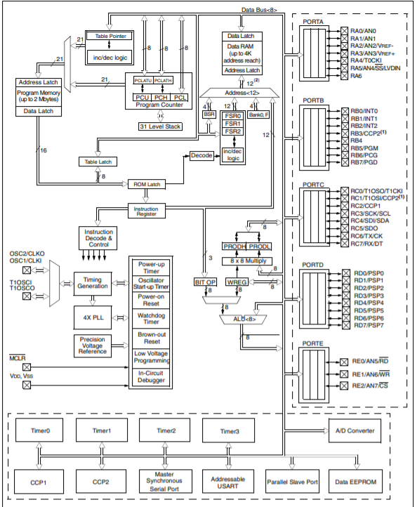
Figure 1. Architecture of PIC controller
The microcontroller architecture consists of CPU, I/O ports, memory organization, A/D converter, timers/counters, interrupts, serial communication, oscillator and CCP module
CPU (Central Processing Unit)
The PIC microcontroller CPU consists of the Arithmetic and Logic Unit, Memory Unit, Control Unit, accumulator and so on.
Arithmetic logic unit are mainly used for arithmetic operations and logical decisions. After processing, for storing the instructions memory is used. To control the internal and external peripherals, control unit is used to connect to CPU and accumulator is used for storing results.
Memory Organization
The memory module consists of RAM, ROM and STACK.
Random Access Memory (RAM)
RAM is an unstable memory used to store data temporarily in its registers. The registers of RAM are classified into Special Function Registers (SFR) and General-Purpose Registers (GPR).
- General Purpose Registers (GPR)
These registers are used for general purpose only.
- Special Function Registers
They are mainly used for special purposes only. These registers perform according to the functions assigned to them,
The STATUS register cannot be used for storing data, these registers are used for showing the operation or status of the program.
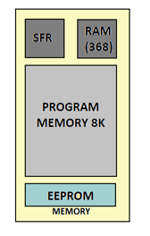
Figure 2. Memory Organization
Read Only Memory (ROM)
Read only memory is a stable memory used to store the data permanently. In PIC microcontroller ROM stores the instructions or programs. The microcontroller acts according to the program.
The ROM is also called as program memory, here the user writes the program and saves it permanently and executed by CPU. The microcontroller’s performance depends on the instruction executed by the CPU.
Electrically Erasable Programmable Read Only Memory (EEPROM)
Normally in ROM, we write the program only once and cannot use it multiple times. But, in EEPROM you can program the ROM multiple times.
Flash Memory
Flash memory also known as programmable read only memory (PROM) can read, write and erase the program thousands of times. PIC microcontroller uses this type of ROM.
Stack
When an interrupt occurs, first the PIC microcontroller must execute the interrupt and the existing process address that is being executed and store it in the stack. After completing the execution of the interrupt, the microcontroller calls the process with the help of address, which is stored in the stack and executes the process.
BUS
BUS is used for transfer and receive of data from one peripheral to another. It is classified into two types that is address and data bus.
Data Bus: It is used to transfer or receive the data.
Address Bus: Address bus transmits the memory address from peripherals to CPU. I/O pins are used to interface with external peripheral. UART and USART are serial communication protocols used for interfacing serial devices like GSM, GPS, Bluetooth, IR, and so on.
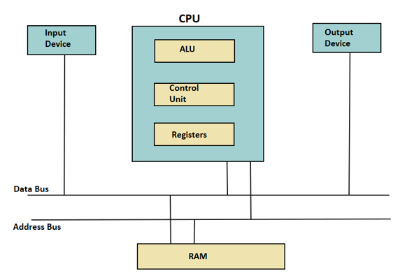
Figure 3. BUS
A/D converters
The analog to digital converter converts analog voltage values to digital voltage values. A/D module of PIC microcontroller consists of 5 inputs of 28 pin devices and 8 inputs of 40 pin devices.
The operation of the analog to digital converter is controlled by special registers ADCON0 and ADCON1. The upper bits of the converter are stored in ADRESH register and lower bits of the converter are stored in ADRESL register. It requires 5V of an analog reference voltage for operation.
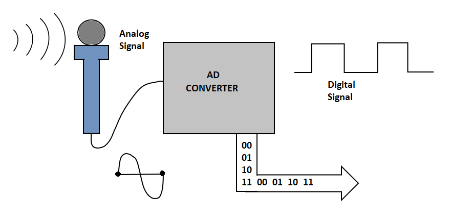
Figure 4. A/D CONVERTER
Timers/ Counters
PIC microcontroller consists of four timer/counters wherein one is 8-bit timer and the remaining timers can be 8 or 16-bit mode. Timers are used for generating accuracy actions, for example, creating specific time delays between two operations.
Interrupts
PIC microcontroller consists of 20 internal interrupts and three external interrupt sources associated with different peripherals like ADC, USART, Timers, and so on.
Serial Communication
Serial communication is the method used for transferring data one bit at a time sequentially over communication channel.
- USART: (Universal synchronous and Asynchronous Receiver and Transmitter)
The two serial communication protocols used for transmitting and receiving data bit by bit over a single wire with respect to clock pulses. The PIC microcontroller has two pins TXD and RXD used for transmitting and receiving the data serially.
- SPI Protocol: (Serial Peripheral Interface)
This protocol is used for sending data between PIC microcontroller and other peripherals which include SD cards, sensors and shift registers.
PIC microcontroller supports three- wire SPI communications between two devices on a common clock source.
- I2C Protocol: (Inter Integrated circuit)
A serial protocol used to connect low speed devices such as EEPROMS, microcontrollers, A/D converters, and so on. PIC microcontroller support two wire Interface or I2C communication between two devices which can work as Master and Slave device.
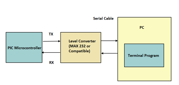
Figure 5. Serial Communication
CCP module
CCP module stands for capture/compare/PWM.
- Capture Mode: Capture mode captures the time of arrival of a signal, that is when the CCP pin goes high, it captures the value of Timer1.
- Compare Mode: Compare mode acts as analog comparator. When timer1 value reaches certain reference value it generates output.
- PWM Mode: PWM mode provides pulse width modulated output with 10-bit resolution and programmable duty cycle.
Key takeaway
The microcontroller architecture consists of CPU, I/O ports, memory organization, A/D converter, timers/counters, interrupts, serial communication, oscillator and CCP module
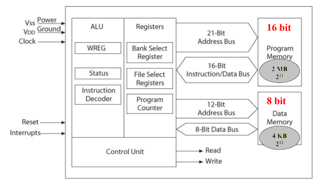
Fig 6 MCU and Memory
Includes Arithmetic Logic Unit (ALU), Registers, and Control Unit and Arithmetic Logic Unit (ALU)
- Performs logical and arithmetic functions
- WREG – working register (acts as an accumulator) – used to perform arithmetic or logical functions
- Status register that stores flags – indicates the status of the operation done by ALU
- Instruction decoder (ID)– when the instruction is fetched it goes into the ID to be interpreted – tell the processor what to do.
Registers – hold memory address
Bank Select Register (BSR)
4-bit register used in direct addressing the data memory.
File Select Registers (FSRs)
16-bit registers used as memory pointers in indirect addressing data memory n Program Counter (PC)
21-bit register that holds the program memory address while executing programs
Control unit- Provides timing and control signals to various Read and Write operations
- Data and Program memory are separated.
- This separation makes a path for simultaneous access of data and instruction.
- Data memory are used as general-purpose registers or special function registers
- In program memory the user writes the program and saves it permanently, which is executed by the CPU. The microcontrollers performance depends on the instruction executed by the CPU.
- On-chip data EPROM are provided in some PIC-18 MCUs
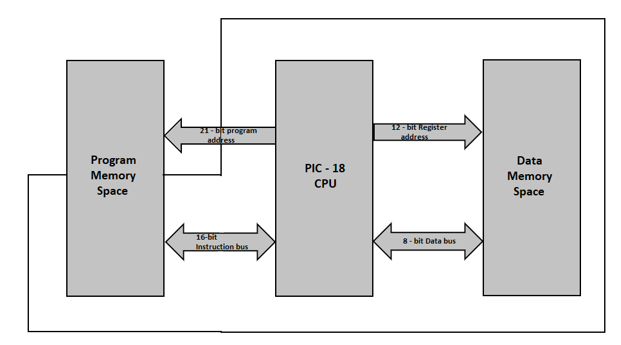
Figure 7. Separation of Data and Program Memory
Data Memory:
- PIC-18 has 4KB Data Memory.
- The data memory is divided into banks and each bank is 256 bytes.
- It consists of GPRs, SFRs referred as Data Registers.
- General purpose registers are used to hold dynamic data.
- SFRs are used to control the operation of Peripheral functions. Only one bank is active at a time.
- Access bank consists of lowest 96bytes and highest 160 bytes of data memory space.
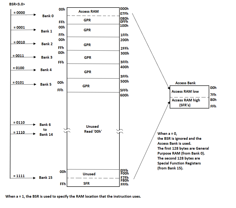
Figure 8. Data Memory map for PIC-18 Device.
- Program Memory Organization:
- The program counter is 21-bit long which enables the user program to access up to 2MB program memory.
- After Power on it starts to execute the instruction from address 0
- The location 0x08 is reserved for high-priority ISR
- The location 0x18 is reserved for low-priority ISR.
- Upto 128KB of Program Memory is inside the MCU chip.
- Rest of the program memory is located outside the MCU chip.
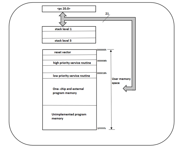
Figure 9. Program Memory Organization for PIC-18 device.
Key takeaway
- PIC-18 has 4KB Data Memory.
- The data memory is divided into banks and each bank is 256 bytes.
- It consists of GPRs, SFRs referred as Data Registers.
- General purpose registers are used to hold dynamic data.
- SFRs are used to control the operation of Peripheral functions. Only one bank is active at a time.
Four banks of Registers/RAM.
- The register/RAM in bank 0 at address between 0x000 and 0x07F
- The register/RAM in bank 1 at address between 0x080 and 0x0FF
- The register/RAM in bank 2 at address between 0x100 and 0x17F
- The register/RAM in bank 3 is at address between 0x180 and 0x1FF.
A byte at an address 0x25 accessed directly by using direct address 0x25 in the instruction. It is considered at bank 0 as 0x25 falls in bank 0 address space.
Direct Address
- A byte at an address 0x85 can be accessed by 7-bit direct address = 0x05 of Bank1
- Bank 1 base address is 0x80 and 0x85–0x80 = 0x05
Bank Pairs
- Four banks form two pairs of banks of Registers/RAM
- The register/RAM in lower bank pair is at address between 0x000 and 0x0FF
- A Bank pair needs 8-bit to access.
- The register/RAM in upper bank pair is at address between 0x100 and 0x1FF
- Bank-pair 0 address is 0x000 and 1 address is 0x100.
Register/RAM Bank Pair access
- By 8-bit address
- Bank pair is as per IRP bit
- 8-bit address is used when using indirect address for a register/RAM
- This address plus the bank-pair base address generates 9-bit address of a register/internal RAM
- Bank pair base address is as per IRP
RAM/File Register Select Register (FSR)
- FSR is used for indirect addressing in the instruction
- FSR of 8-bits
- It provides the 8-bit address of RAM/register in register file
- That address is in a bank-pair
- Bank pair is as per IRP bit in the STATUS.
IRP (indirect register-bank pair) bit
- Indirect address has 8-bits.
- These bits are taken from either lower pair of banks 0 or 1 or upper pair of banks 2 or 3
- Bit 7 in STATUS, when = 1, then upper bank-pair used
- When = 0 then lower bank pair used.
RP1-RP0 (register- pair higher bank register pair lower bank) bits
- Direct address has taken from 7-bits in the instruction
- They are taken for either bank 0 or 1 or 2 or 3.
- Bit 6-5 in STATUS, when = 11, then higher bank 3. When = 10, then bank 2. When = 01, then bank 1. When = 00, then bank 0.
Higher addresses Mirroring in all four banks
- Higher addresses 0x70-0x7F in a bank are also mirrored.
- When 0x70-0x7F is accessed, then it also means access to 0xF0H-0xFFH, 0x170-0x17F and 0x1F0-0x1FF.
- Frequently used variables are stored at these sixteen addresses by the programmer
Key takeaways
- Register File/RAM 368 Bytes
- 9-bit address
- Address generates by 7-bit direct address in the instruction or
- Address generates by 8-bit indirect address in in File Select Register
- Register file of 368 bytes divides in four banks
- Bank has 128 bytes each
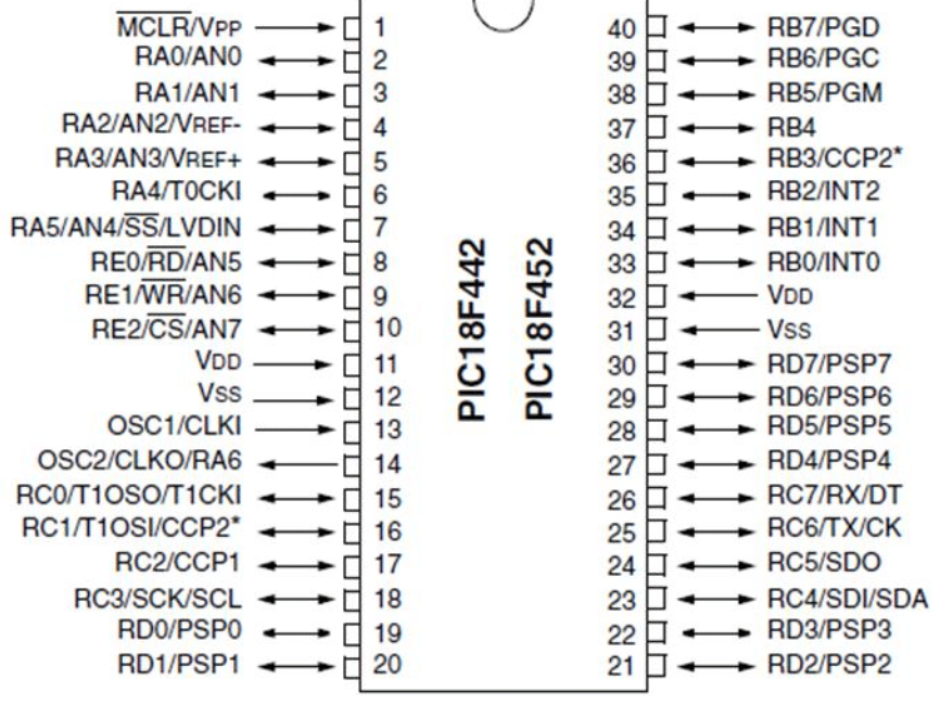
Figure 10. Pin Diagram
Pin 1 | MCLR /Vpp | MCLR – Master Clear (Reset) input. This pin is active low RESET to the device.
Vpp- High voltage ICSP programming enable pin.
|
Pin 2 | RA0/AN0 | RA1-Digital I/O ANO-analog input 0 |
Pin 3 | RA1/AN1 | RA1- Digital I/O AN1 -analog input 1 |
Pin 4 | RA2/AN2/Vref- | RA2- Digital I/O AN2- analog input 2 Vref – A/D reference voltage (low) input. |
Pin 5 | RA3/AN3/Vref+ | RA3- Digital I/O AN3- analog input 3 Vref+- A/D reference voltage (high) input. |
Pin 6 | RA4/ T0CK1 | RA4- Digital I/O T0CK1- Timer 0 external clock input. |
Pin 7 | RA5/AN4/SS/LVDIN | RA5- Digital I/O Analog input 4 |
|
| SS- SPI Slave Select Input. Low Voltage Detect Input.
|
Pin 8 | RE0/RD/AN5 | Port E – bi-directional port AN5-Analog input 5 RD – Read control for parallel slave port. RE0- Digital I/O
|
Pin 9 | RE1/WR/AN6 | RE1-Digital I/O WR- Write control for parallel slave port AN6-Analog input 6 |
Pin 10 | RE2/CS/AN7 | RE2- Digital I/O CS– chip select AN7- Analog input 7 |
Pin 11 | VDD | Supply |
Pin 12 | VSS | Ground |
Pin 13 | OSC1/CK1 | Oscillator crystal input or external clock source. CK1- external clock source input. |
Pin 14 | OSC2/CK0/RA6 | OSC2- Oscillator crystal output. Connects to crystal or resonator in crystal oscillator mode. In RC mode OSC2 pin outputs CLK0 which has ¼ the frequency of OSC1 and denotes the instruction cycle rate. RA6 – General purpose pin.
|
Pin 15 | RC0/T1OSO/T1CK1 | Port C is directional port RCO- Digital I/O T1OSO- Timer 1 oscillator output T1CK1- Timer1 / Timer 3 external clock input. |
Pin 16 | RC1/T1OS1/CCP2 | RC1- Digital I/O T1OS1- Timer 1 oscillator input CCP2- Capture 2 input. Compare 2 output, PWM 2 output. |
Pin 17 | RC2/CCP1 | RC2- Digital I/O CCP1- Capture 1 input. Compare 1. PWM1 output. |
Pin 18 | RC3/SCK/SCL | RC3- Digital I/O SCK- Synchronous serial clock input/output for SPI mode SCL- Synchronous serial clock input/output for I2C mode. |
Pin 19 | RD0/PSP0 | Port D is bidirectional port. RD0 –Digital I/O PSP0- Parallel Slave port data. |
Pin 20 | RD1/PSP1 | RD1- Digital I/O PSP1- Parallel Slave port data |
Pin 21 | RD2/PSP2 | RD2- Digital I/O PSP2- Parallel slave port data |
Pin 22 | RD3/PSP3 | RD3- Digital I/O PSP3- Parallel slave port data. |
Pin 23 | RC4/SDI/SDA | RC4- Digital I/O SDI- SPI Data IN SDA- I2C Data I/O |
Pin 24 | RC5/SD0 | RC5-Digital I/O SD0- SPI Data out |
Pin 25 | RC6/TX/CK | RC6- Digital I/O TX- USART Asynchronous Transmit CK- USART Synchronous clock |
Pin 26 | RC7/RX/DT | RC7-Digital I/O RX- USART Asynchronous Receive DT- USART Synchronous Data |
Pin 27 | RD4/PSP4 | RD4- Digital I/O PSP4- Parallel slave port data |
Pin 28 | RD5/PSP5 | RD5- Digital I/O PSP5- Parallel slave port data |
Pin 29 | RD6/PSP6 | RD6- Digital I/O PSP6- Parallel slave port data |
Pin 30 | RD7/PSP7 | RD7- Digital I/O PSP7- Parallel slave port data |
Pin 31 | Vss | Ground |
Pin 32 | Vdd | Supply voltage |
Pin 33 | RB0/INTO | RB0- Digital I/O INTO – External Interrupt 0 |
Pin 34 | RB1/INT1 | RB1- Digital I/O INT1- External Interrupt 1 |
Pin 35 | RB2/INT2 | RB2- Digital I/O INT2- External Interrupt 2 |
Pin 36 | RB3/CCP2 | RB3- Digital I/O CCP2- Capture 2 input. Compare 2 output. PWM2 output. |
Pin 37 | RB4 | RB4-Digital I/O. Interrupt on change pin. |
Pin 38 | RB5/PGM | RB5-Digital I/O. Interrupt on change pin. PGM – Low Voltage Programming enable pin.
|
Pin 39 | RB6/ PGC | RB6- Digital I/O. Interrupt on change pin. PGC- In-circuit debugger and programming clock pin. |
Pin 40 | RB7/PGD | RB7- Digital I/O. Interrupt on change pin. PGD- In-circuit debugger and programming data pin. |
Reset keeps the microcontroller into known condition. For microcontroller to function properly it must be reset which means all the registers would be placed in starting position. It can be used to when trying out a device as interrupt in program execution.
For proper operation MCLR pin must be connected via resistor to positive supply. The resistor value varies between 5 and 10K. The function of the resistor is to keep certain line on logical one as preventive called as pull- up resistor.
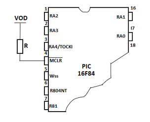
Figure 11. Reset
Watchdog timer is a hardware microcontroller. It is basically used to take out a system from an infinite loop and resets the system. Watchdog makes the embedded systems more reliable as it works as a safety mechanism.
Watchdog is a type of counter. It is an up counter which means that it counts from zero and reaches to some values. As soon the watchdog timer reaches some value its hardware generates a watchdog reset. Then the system resets this count value to zero in order to avoid system reset. The watchdog timer is loaded with some values which are based on its timeout time. The system needs to reset the counter before timeout.
Watchdog Timer Hardware
The figure below is of watchdog time hardware with input as clock. With every clock the internal counter increments. Then the comparator will compare this value with the loaded count value. Then if the comparator finds that count value matches the watchdog hardware generates and resets it.
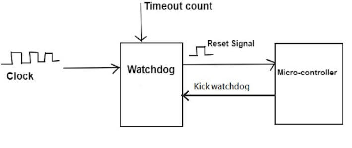
Fig 12 Watch dog timer
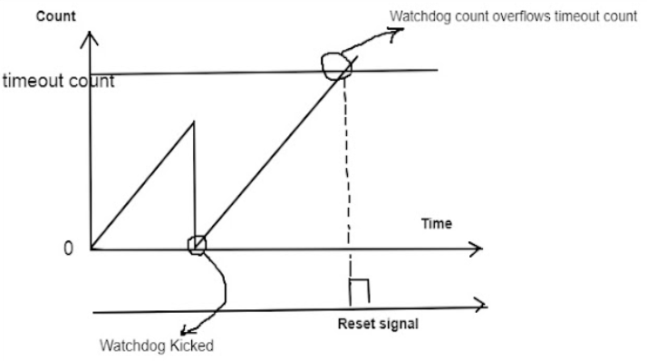
Fig 13 Timing Diagram
Watchdog in Microcontroller
The internal watchdog of the MSP430 family is used either as a simple timer or as a watchdog that ensures system integrity. The watchdog function is enabled after power-on reset or system reset. In case of any difficulties after start-up of MSP430, the watchdog will reset the system as often as it is needed for it to start successfully.
A system running with MCLK = 3 MHz uses the watchdog for supervision of three functions.
Power Fail — by checking the 60 Hz AC line.
Function 1 — A check is made if the software reaches this background part regularly
Function 3 — A check is made if this interrupt handler is called regularly.
Each supervised function sets a dedicated bit in RAM byte WDB in intervals less than 10.66 ms (power-up value of the watchdog with MCLK = 3 MHz) if everything is functioning normally.
The main loop checks this byte (WDB) and resets the watchdog ONLY if all three bits are set (07h). If one of the functions fails, the watchdog is not reset and will therefore reset the system.
Key takeaway
Watchdog timer is a hardware microcontroller. It is basically used to take out a system from an infinite loop and resets the system. Watchdog makes the embedded systems more reliable as it works as a safety mechanism.
- Oscillators are used for timing generation. PIC microcontroller consists of external oscillators like RC oscillators or crystal oscillators.
- The crystal oscillator is connected between two oscillator pins. The value of the capacitor connected to every pin decides the mode of operation of the oscillator.
- In case of RC oscillators, the value of the resistor & capacitor determines the clock frequency and the range of clock frequency is 30KHz to 4MHz.
- In calculating software delays in pic microcontroller, the instruction execution time is determined by external clock either in oscillator or resonator.
The PIC18FXX2 operates in eight oscillator modes differently. The user can program three configuration bits (FOSC2, FOSC1, and FOSC0) and select one of these eight modes:
1. LP Low Power Crystal
2. XT Crystal/Resonator
3. HS High Speed Crystal/Resonator
4. HS + PLL High Speed Crystal/Resonator with PLL enabled
5. RC External Resistor/Capacitor
6. RCIO External Resistor/Capacitor with I/O pin enabled
7. EC External Clock
8. ECIO External Clock with I/O pin enable
Power Down modes
In sleep or power down mode PIC microcontroller is placed in its lowest current consumption state. The device goes to sleep mode by executing SLEEP instruction. The device oscillator is turned off, so no system clocks are occurring in the device.
In order to minimize the power consumption in sleep mode the output ports must be sourcing or sinking the current before going to sleep mode.
Several events make the device wake up from sleep mode:
- Any device reset.
- Watch dog timer Wake-up
- Peripheral module which can set its interrupt flag while in sleep.
- Configuration bit settings
Every single bit in this register controls a specific feature, combined in this register to control all the settings (configurations), Hence they are often called the “Configuration Bits” referred as “Fuses” sometimes.
It allows the programmer to adjust to certain conditions in order to determine the operation modes of microcontroller. This state of configuration bits determines the mode in which device operates when powered.
These configuration bits are mapped to the program memory location which can be accessed at the time of programming.
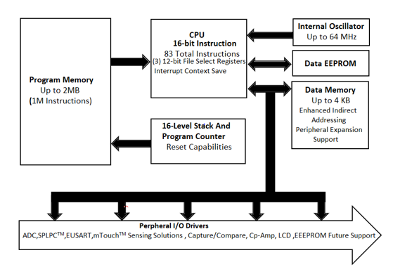
Figure 14. Peripherals
The PIC18 family combines maximum level of performance and integration for flexible use of 8-bit architecture.
- Internal Oscillator Up to 64 MHz.
- Flash Program Memory Up to 128 kB.
- Data EEPROM Up to 1 kB.
- SRAM Up to 8 kB.
- 32 Level Stack
- Hardware Stack Overflow and Underflow Reset Capabilities
- Vectored Interrupt Capability (VIC)
- Direct Access Memory (DAM) Controllers
- 12-bit ADC with Computation (ADC2), up to 43 channels
- Memory Access Partition (MAP)
- Device Information Area (DIA)
- Windowed Watch Dog Timer (WWDT)
- Three Complementary Waveform Generator (CWG)
- Four Configurable Logic Cell (CLC)
- Peripheral Pin Select (PPS)
- Two Comparators
- Zero Cross Detect (ZCD)
- Temperature Indicator On-chip
- Data Signal Modulator (DSM)
- 5-bit DAC
- Capacitive Voltage Divider (CVD)
- Up to four 10-bit PWMs
- Communication: UART, SPI, I2C, CAN, USB, Ethernet, LCD
- Extreme Low-Power (XLP)
- Available in 18- to 100-pin Package
The PIC 18F is divided into seven groups:
- Move (Data Copy) and Load
- Logical
- Branch or Jump
- Bit Manipulation
- Table Read or Write
- Machine Control.
- Move and Load Instructions:
MOVLW 8-bit; Load an 8-bit literal in WREG
MOVLW 0 x F2
MOVWF F, a; Copy WREG in File (Data) Reg
If a=0, F is in Access bank
If a = 1 Bank is specified by BSR
MOVWF 0X25,0; Copy W in data Reg 25H
MOVFF fs, fd; Copy from one Data Reg to another data register
MOVFF 0x20,0x30; Copy Data Reg 20 into Reg 30.
2. Arithmetic Instructions
ADDLW 8-bit; Add 8-bit number to WREG
ADDLW 0x32; Add 32H to WREG
ADDWF F, d, a; Add WREG to File (Data) Reg
Save result in W if d=0
Save result in F if d=1
ADDWF 0x20, 1; Add WREG to REG20 and save result in REG20
ADDWF 0X20,0; Add WREG to REG20 and save result in WREG
ADDWFC F, d, a; Add WREG to File Reg with carry and save result in W or F
SUBLW; Subtract WREG from literal
SUBWF F, d, a; Subtract WREG from File Reg
SUBWFB; Subtract WREG from File Reg with borrow
INCF; Increment File Reg
DECF; Decrement File Reg
COMF ; Complement File Reg
NEGF; Take two’s complement.
MULLW 8-bit; Multiply 8-bit and WREG save in PRODH -PRODL
MULWF F, a; Multiply WREG and File Reg save result in PRODH-PRODL
DAW; Decimal adjust WREG for BCD operations.
3. Logic Instructions:
ANDLW; AND literal with WREG
ANDWF F, d, a
IORLW 8-bit dats; Inclusive OR literal with WREG
IORWF F, d, a
XORLW 8-bit; Ex-clusive OR literal with WREG.
XORWF F, d, a
4. Branch Instructions
- BC n; Branch if C flag = 1 within + or – 64 Words
- BNC n; Branch if C flag = 0 within + or – 64 Words (NO CARRY)
- BZ n; Branch if Z flag = 1 within + or – 64 Words
- BNZ n; Branch if Z flag = 0 within + or – 64 Words
- BN n; Branch if N flag = 1 within + or – 64 Words
- BNN n; Branch if N flag = 0 within + or – 64 Words
- BOV n; Branch if OV flag = 1 within + or – 64 Words
- BNOV n; Branch if OV flag = 0 within + or – 64 Words
- GOTO Address: Branch to 20-bit address unconditionally
5. Call and Return Instructions
- RCALL nn; Call subroutine within +or – 512 words
- CALL 20-bit, s; Call subroutine; If s = 1, save W, STATUS, and BSR
- RETURN, s; Return subroutine o; If s = 1, retrieve W, STATUS, and BSR
- RETFIE, s; Return from interrupt o; If s = 1, retrieve W, STATUS, and BSR
6. Bit Manipulation Instructions
- BCF F, b, a; Clear bit b of file register. b = 0 to 7
- BSF F, b, a; Set bit b of file register. b = 0 to 7
- BTG F, b, a; Toggle bit b of file register. b = 0 to 7
- RLCF F, d, a; Rotate bits left in file register through; carry and save in W or F register
- RLNCF F, d, a; Rotate bits left in file register; and save in W or F register
- RRCF F, d, a; Rotate bits right in file register through o; carry and save in W or F register
- RRNCF F, d, a; Rotate bits right in file register; and save in W or F register
7. Table Read and Write Instructions:
- TBLWT*; Write TABLAT into Program Memory pointed; by TBLPTR
- TBLWT*+; Write TABLAT into Program Memory pointed; by TBLPTR and increment TBLPTR
- TBLWT*-; Write TABLAT into Program Memory pointed; by TBLPTR and decrement TBLPTR
- TBLWT+*; Increment TBLPTR and Write TABLAT into; Program Memory pointed by TBLPTR
8. Machine Control Instructions
CLRWDT; Clear Watchdog Timer n Helps recover from software malfunction n Uses its own free-running on-chip RC oscillator n WDT is cleared by CLRWDT instruction
- RESET; Reset all registers and flags n When voltage < a particular threshold, the device is held in reset n Prevents erratic or unexpected operation
- SLEEP; Go into standby mode
- NOP; No operation
References:
1. Kenneth J. Ayala, ‘The 8051 Microcontroller Architecture, Programming and Applications’, Cengage Learning, 3rd Edition
2. Ajay Deshmukh, “Microcontrollers Theory and Applications”, TATA McGraw Hill, 4th Edition
3. Peatman, John B, “Design with PIC Microcontroller”, Pearson Education PTE, 1st Edition
4. Data Sheet of PIC 18Fxxxx series