Unit - 4
Peripheral Support in PIC 18FXXXX
Timers are used to measure time or generate accurate time delay. Timer is a binary counter configured to count clock pulses. Once it reaches maximum value it rolls back to zero. It sets an overflow flag and generate interrupt if enabled.
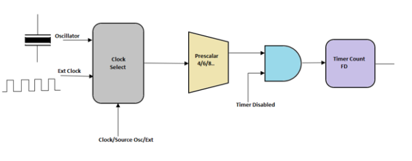
Figure 1. Timer Block Diagram
PIC18F4520 has three independent timer which can be used as timer, counters or for PWM generation.
- Timer 0 8-bit
- Timer 1 16-bit
- Timer 2 8 bit
Calculation:
PIC oscillator frequency is divided by 4 and fed to the controller.
This frequency is further sub-divided by pre-scalar to generate range of delays.
The time to increment the timer count by one can be determined as below:
Tick = (Pre-scalar/(Fosc/4)
Tick = (Pre-scalar/(20Mhz/4))
$$ tick = (Pre-scalar * 4) / Fosc $$
Now the timer value for required delay can be calculated as shown:
Delay = TimerCount * tick
Count = (Delay/tick)
RegValue = TimerMax – Count
RegValue = TimerMax-(Delay/tick) = TimerMax-(Delay/ (Pre-scalar *4)/Fosc))
$$RegValue = TimerMax-((Delay*Fosc)/Pre-scalar*4)) $$
TIMER0 8-bit $$RegValue = 256-((Delay * Fosc)/(Pre-scalar*4)) $$
TIMER1 16-bit $$RegValue = 65536-((Delay * Fosc)/(Pre-scalar*4)) $$
TIMER2 8-bit $$RegValue = 256-((Delay * Fosc)/(Pre-scalar*4)) $$
Timer 0
The TMR0 module is an 8-bit timer/counter with the following features:
- 8-bit timer/counter
- Readable and writable
- 8-bit software programmable pre-scaler
- Internal or external clock select
- Interrupt on overflow from FFh to 00h
- Edge selects for external clock
Timer 0 Register
Register | Description |
OPTION_REG | This registers is used to configure the TIMER0 Prescalar, Clock Source |
TMR0 | This register holds the timer count value which will be incremented depending on prescalar configuration |
INTCON | This register contains the Timer0 over flow flag(TMER0IF) and corresponding Interrupt Enable flag(TMR0IE) |
OPTION_REG | ||||||
7 | 6 | 5 | 4 | 3 | 2 | 1 |
RBPU | INTEDG | T0CS | T0SE | PSA | PS2 | PS1 |
RBPU: NA for Timers
INTEDG: NA for Timers
T0CS: TMR0 Clock Source Select bit
1-Transition on T0CKI pin
0-Internal instruction cycle clock (CLKO)
T0SE: TMR0 Source Edge Select bit
1-Increment on high-to-low transition on T0CKI pin
0-Increment on low-to-high transition on T0CKI pin
PSA: Pre-scaler Assignment bit
1-Prescaler is assigned to the WDT
0-Prescaler is assigned to the Timer0
PS2:PS0: Pre-scalar rate select bits.
BIT VALUE | TMR0 RATE | WDT RATE |
000 | 1:2 | 1:1 |
001 | 1:4 | 1:2 |
010 | 1:8 | 1:4 |
011 | 1:16 | 1:8 |
100 | 1:32 | 1:16 |
101 | 1:64 | 1:32 |
110 | 1:128 | 1:64 |
111 | 1:256 | 1:128 |
INTCON |
| ||||||
7 | 6 | 5 | 4 | 3 | 2 | 1 | 0 |
GIE | PIE | TMR0E | INTTE | RBIE | TMR0IF | INTF | RBIF |
GIE: Global Interrupt Enable bit
1-Enables all unmasked interrupts
0-Disables all interrupts
PIE: Peripheral Interrupt Enable bit
1-Enables all unmasked peripheral interrupts
0-Disables all peripheral interrupts
TMR0IE: TMR0 Overflow Interrupt Enable bit
1-Enables the TMR0 interrupt
0-Disables the TMR0 interrupt
INTE: NA for Timers
RBIE: NA for Timers
TMR0IF: TMR0 Overflow Interrupt Flag bit
1-TMR0 register has overflowed (must be cleared in software)
0-TMR0 register did not overflow
INTF: NA for Timers
RBIF: NA for Timers
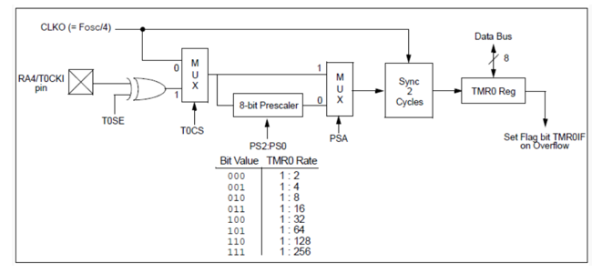
Figure 2 Timer 0 Block Diagram excluding WDT
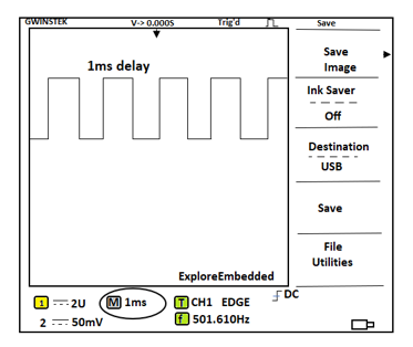
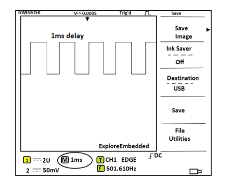
Delay Calculations for 1ms @20Mhz with Pre-scalar as 32: $$RegValue = 256-(Delay * Fosc)/(Pre-scalar*4)) = 256-((1ms * 20Mhz)/ (32*4)) = 256-156=100$$.
Code:
Steps for configuring and using the Timer0 for delay generation:
- For delay calculation use TimerCount.
- Set the Pre-scalar bits in OPTION_REG as per the delay calculations.
- Clear the PSA bit for using the pre-scalar.
- Select the Clock Source Internal/External using TOCS bit.
- Load the timer value into TMRO register.
- Enable the Timer0 Interrupt by setting TMR0IE bit
- Enable the Global and Peripheral interrupts by setting GIE and PIE bits.
Sample code to blink the LEDs with 1ms delay
#include<pic16f877a.h>
Char value = 0;
#define SBIT_PS2 2
Void interrupt timer_isr()
{
If(TMR0IF==1)
{
Value=~value; // complement the value for blinking the LEDs
TMR0 = 101; /*Load the timer Value, (Note: Timervalue is 101 instaed of 100 as the
TImer0 needs two instruction Cycles to start incrementing TMR0 */
TMR0IF=0; // Clear timer interrupt flag
}
}
Void main()
{
TRISD=0x00; //COnfigure PORTD as output to blink the LEDs
OPTION_REG = (1<<SBIT_PS2); // Timer0 with external freq and 32 as prescalar
TMR0=100; // Load the time value for 1ms delay
TMR0IE=1; //Enable timer interrupt bit in PIE1 register
GIE=1; //Enable Global Interrupt
PEIE=1; //Enable the Peripheral Interrupt
While(1)
{
PORTD = value;
}
}
Output:
Timer 1
The timer TMR1 module is 16-bit timer/counter with features such as:
- 16-bit timer/counter with two 8-Bit register TMR1H/TMR1L
- Writeable and Readable
- Software programmable pre-scaler upto 1:8
- Internal or external clock select
- Interrupt on overflow from FFFFh to 00h
- Edge selects for external clock.
Timer 1 Register
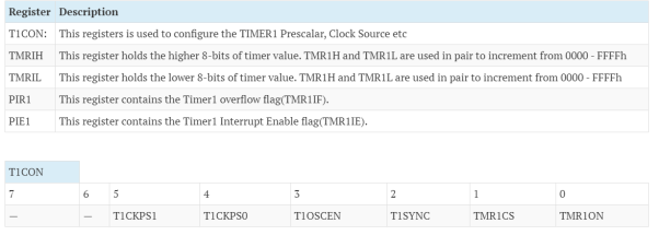
T1CKPS1:T1CKPS0: Timer1 Input Clock Pre-scale Select bits
11 = 1:8 pre-scale value
10 = 1:4 pre-scale value
01 = 1:2 pre-scale value
00 = 1:1 pre-scale value
T1OSCEN: Timer1 Oscillator Enable Control bit
1-Oscillator is enabled
0-Oscillator is shut-off
T1SYNC: Timer1 External Clock Input Synchronization Control bit
1-Do not synchronize external clock input
0-Synchronize external clock input
TMR1CS: Timer1 Clock Source Select bit
1-External clock from pin RC0/T1OSO/T1CKI (on the rising edge)
0-Internal clock (FOSC/4)
TMR1ON: Timer1 On bit
1-Enables Timer1
0-Stops Timer1
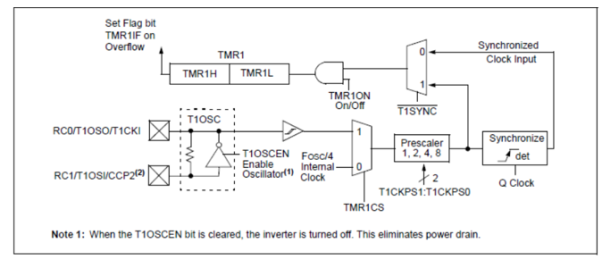
Fig 3 Timer 1 Block Diagram
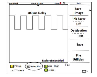
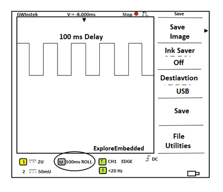
Delay Calculations for 100ms @20Mhz with Prescalar as 8: $$RegValue = 65536-(Delay * Fosc)/(Prescalar*4)) = 65536-((100ms * 20Mhz)/(8*4)) = 3036 = 0xBDC$$
Code:
Steps to configure by using the Timer1 for delay generation:
- Calculate the Timer Count for required delay.
- Set the Pre-scalar bits in T1CON as per the delay calculations.
- With the help of TMR1CS bit Select the Clock Source Internal/External
- Load the timer value into registers TMR1H, TMR1L.
- For Enabling the Timer1 Interrupt set TMRIE bit
- For Enabling the Global and Peripheral interrupts set GIE and PIE bits.
- Start the timer by setting TMR1ON bit.
#include<pic16f877a.h>
Char value = 0;
#define SBIT_PS1 5
#define SBIT_PS0 4
Void interrupt timer_isr()
{
If(TMR1IF==1)
{
Value=~value; // complement the value for blinking the LEDs
TMR1H=0x0B; // Load the time value(0xBDC) for 100ms delay
TMR1L=0xDC;
TMR1IF=0; // Clear timer interrupt flag
}
}
Void main()
{
TRISD=0x00; //COnfigure PORTD as output to blink the LEDs
T1CON = (1<<SBIT_PS1) | (1<<SBIT_PS0); // Timer0 with external freq and 8 as prescalar
TMR1H=0x0B; // Load the time value(0xBDC) for 100ms delay
TMR1L=0xDC;
TMR1IE=1; //Enable timer interrupt bit in PIE1 register
GIE=1; //Enable Global Interrupt
PEIE=1; //Enable the Peripheral Interrupt
TMR1ON = 1; //Start Timer1
While(1)
{
PORTD = value;
}
}
Output:
Key takeaway
Timers are used to measure time or generate accurate time delay. Timer is a binary counter configured to count clock pulses. Once it reaches maximum value it rolls back to zero. It sets an overflow flag and generate interrupt if enabled.
Interrupts in PIC18F family is divided into two groups: high and low priority. Applications that require more attention can be placed in higher priority group. A high priority interrupt can stop the low-priority interrupt that is in progress and gain access to CPU. High-priority interrupts can be stopped by low-priority interrupts.
Every interrupt source has three bits to control its operation:
- A flag bit to indicate whether an interrupt has occurred regardless of whether it is enabled or not.
- Interrupt enable bit to enable or disable interrupt source.
- A priority bit to select high or low priority.
The following conditions must be satisfied for an interrupt to work:
- The interrupt enable bit of the interrupt source must be enabled. Consider an interrupt source is external interrupt pin INT0 then INT0IE of register INTCON must be set to 1.
- The interrupt flag of interrupt source must be cleared. Consider if the external interrupt pin INTO then bit INT0IF of register INTCON must be cleared to 0.
- The peripheral interrupt enable/disable bit PEIE of INTCON must be set to 1 if the interrupt source is peripheral.
- The global interrupt enable/disable bit of GIE of INTCON must be set to 1.
RCON – Reset Control Register

Bit 7 | IPEN: Interrupt Priority Enable bit
1- Enable priority levels on interrupts 0- Disable priority levels on interrupts
|
Bit 6 | SBOREN- BOR Software Enable bit If BOREN1:BOREN0=01 1- BOR is enabled 0 – BOR is disabled. If BOREN 1: BOREN0 = 00,10 or 11: Bit is disabled and read as ‘0’
|
Bit 5 | Unimplemented: Read as ‘0’ |
Bit 4 | RI: RESET Instruction Flag bit
1-Reset Instruction was not executed
0- RESET instruction was executed causing a device Reset.
|
Bit 3 | TO- Watchdog Time-out Flag bit 1- Set by power up CLRWDT instruction or SLEEP instruction 0 - A WDT time-out occurred. |
Bit 2 | PD – Power-Down Detection Flag bit
1-Set by power-up or by the CLRWDT instruction 0- Set by execution of the SLEEP instruction |
Bit 1 | POR – Power-on Reset Status bit 1- Power-on-Reset has not occurred 0- Power-on-Reset has occurred |
Bit 0 | BOR – Brown-out Reset Status bit 1- Brown -out Reset has not occurred 0 – Brown-out Reset has occurred. |
INTCON Register
INTCON registers are used to configure the external PIC interrupts.

GIE: Global Interrupt Enable
This bit is set high to enable all interrupts of PIC 18F452
1-Enable all interrupts
0- Disable all interrupts
PEIE: Peripheral Interrupt Enable
This bit is set high to enable all peripheral interrupts of the microcontroller.
1- Enable all peripheral interrupts
0 – Disable all peripheral interrupts.
TOIE – TMR) Overflow Interrupt Enable
This bit is set high to enable External Interrupt 0
1 – Enable TMRO overflow interrupt
0 – Disable TMR0 overflow interrupt
INTE: INT External Interrupt Enable
This bit is set to enable external interrupts
1-Enable the INT external interrupt
0 – Disable the INT external interrupt
RBIE: RB Interrupt enable
This bit is set high to enable the RB port Change interrupt pin.
1 – Enables the RB port change interrupt
0 - Disables the RB port change interrupt
T0IF: TMR0 Overflow Interrupt Flag
1 – TMR0 register has overflowed
0 – TMR0 register has not overflowed
INTF: INT External Interrupt Flag
1 – INT external interrupt occurred
0 – INT external interrupt did not occur.
RBIE – RB port Change Interrupt Flag
1 – At least one of the RB7:RB4 pins changed the state
0 – Disables the RB port change interrupt.
T0IF: TMR0 Overflow Interrupt flag
1- TMR0 register has overflowed.
0 – TMR0 has not overflowed.
INTF: INT External Interrupt flag
1 –The INT external interrupt occurred.
0 – The INT external interrupt has not occurred.
RBIF: RB port change interrupt priority
1 - At least one of the RB7:RB4 pins changed the state
0 – None of the pins have changed the state.
INTCON2 Register:

RBPU: Port B Pull up Enable
1= All port B pull ups are diabled
0=All port b pull ups are enabled by individual port latch values
INTEDG0, INTEDG1, INTEDG2: External Interrupt Edge
These bits are used to select the triggering edge of the corresponding interrupt signal on which the microcontroller is to respond.
1=interrupt on rising edge
0= interrupt on falling edge
Bit 3, Bit 1: Unimplemented
It is always read as 0
TMR0IP: TMR0 overflow priority
1=High Priority
0=Low Priority
RBPIP: RB Port change Interrupt Priority
1=High Priority
0=Low Priority
INTCON3 Register:

INT1IP, INT2IP
These bits are used to set priority of the interrupts 1 and 2, respectivey
1=High Priority
0=Low Priority
Bit5, Bit 2:
Both are unimplemented and read as 0
INT1IE, INT2IE
These bits enable/disable the External Interruppt 1 and 2, respectively.
1=Enables the External Interrupt x
0=Disables the External Interrupt x
INT1IF, INT2IF
These are External Interrupt 1 and 2 flag bits, respectively.
1=The INTx External Interupt occurred (must be cleared in software)
0= The INTx External Interupt did not occurred
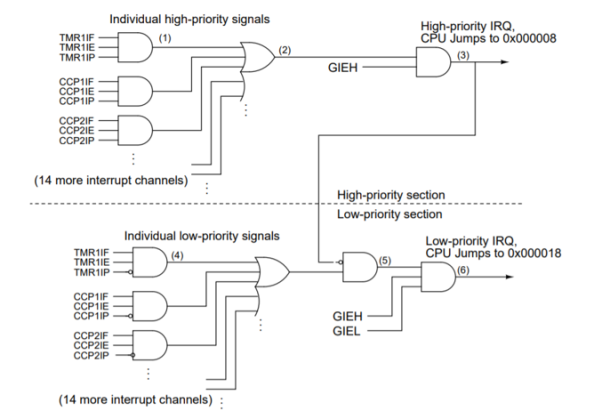
Figure 4. Interrupts in PIC
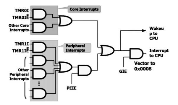
Figure 5. Legacy Interrupt
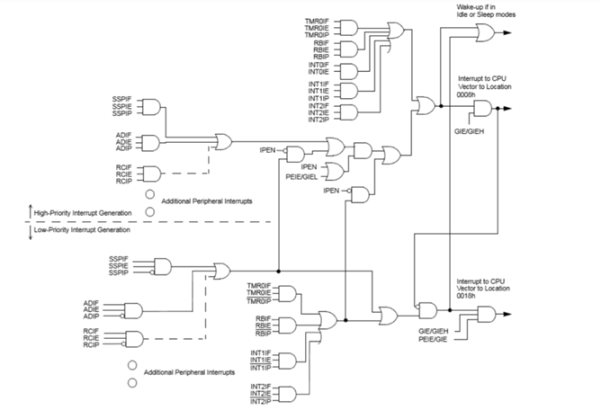
Figure 6. Priority Mode
Interrupt Sources
- 3 or 4 External Interrupts (INT0-INT3)
- Edge Triggered
- Rising or Falling selected in INTCON2 register
- PORTB Interrupt on Change (RB4-RB7)
- Timer Rollover/Overflow Events
- Comparator Output Change
- A/D Conversion Complete
- Communication Channel Events
This “interrupt on change” is triggered when any of the RB7:RB4 pins, configured as an input, changes level. When this interrupt is used in conjunction with the software programmable weak internal pull-ups, a direct interface to a keypad is possible. This is shown in application note AN552, Implementing Wake-up on Key Stroke. Another way to use the “interrupt on change” feature would be as additional external interrupt sources. This allows PIC16CXXX devices to support multiple external interrupts, in addition to the built-in external interrupt on the INT pin.
The interrupt source(s) cannot simply be directly connected to the PORTB pins, and expect an interrupt to occur the same as on the interrupt (INT) pin. To develop the microcontrollers hardware/software to act as an interrupt by an external signal, we must know the characteristics of the external signal. After we know this, we can determine the best way to structure the program to handle this signal. The characteristics that we need to consider when developing the interrupt include:
1. The rising edge and falling edges.
2. The pulse width of the interrupt trigger (high time / low time).
It is easy to understand the need of knowing about which edge triggers the interrupt service routine for the external interrupt. This allows one to ensure that the interrupt service routine is only entered for the desired edge, with all other edges ignored. Not so clear is the pulse width of the interrupt’s trigger. This characteristic helps determine the amount of additional overhead that the software routine may need.
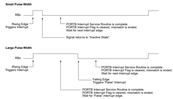
Figure 7 Interrupt steps for small and wide pulse widths
Figure above shows the two cases for the interrupt signal verses the time to complete the interrupt service routine. The first waveform is when the signal makes the low-to-high-to-low transitions before the interrupt service routine has completed (interrupt flag cleared). When the interrupt flag has been cleared, the interrupt signal has already returned to the inactive level. The next transition of the signal is due to another interrupt request. An interrupt signal with this characteristic will be called a small pulse width signal. The second waveform is when the signal only makes the low-to-high transitions before the interrupt service routine has completed (interrupt flag cleared). The next transition (high-to-low) will return the interrupt signal to the inactive level. This will generate a “false” interrupt, that will need to be cleared. Then the following transition (low-to-high) will be a “true” interrupt. An interrupt signal with this characteristic will be called a wide pulse width signal.
An interrupt pulse with a small pulse width requires less overhead than a wide pulse width. A small pulse width signal must be less than the minimum execution time of the interrupt service routine, while a wide pulse width must be greater then, the maximum time through the interrupt service routine.
Timer

Fig 8. Timer Block diagram
PIC18F4520 has three independent timer which can be used as timer, Counters or for PWM generation.

Now the Timer value for the required delay can be calculated as below.
Delay = TimerCount * tick
Count = (Delay/tick)
RegValue = TimerMax- Count
RegValue = TimerMax-(Delay/tick) = TimerMax - (Delay/ ((Prescalar *4)/Fosc))
$$RegValue = TimerMax-((Delay * Fosc)/(Prescalar*4)) $$
Timer 0
The TMR0 module is an 8-bit timer/counter with the following features:
- 8-bit timer/counter
- Readable and writable
- 8-bit software programmable prescaler
- Internal or external clock select
- Interrupt on overflow from FFh to 00h
- Edge selects for external clock
Timer 0 Register

RBPU: NA for Timers
INTEDG: NA for Timers
T0CS: TMR0 Clock Source Select bit
1-Transition on T0CKI pin
0-Internal instruction cycle clock (CLKO)
T0SE: TMR0 Source Edge Select bit
1-Increment on high-to-low transition on T0CKI pin
0-Increment on low-to-high transition on T0CKI pin
PSA: Pre-scaler Assignment bit
1-Prescaler is assigned to the WDT
0-Prescaler is assigned to the Timer0
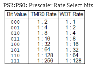

GIE: Global Interrupt Enable bit
1-Enables all unmasked interrupts
0-Disables all interrupts
PIE: Peripheral Interrupt Enable bit
1-Enables all unmasked peripheral interrupts
0-Disables all peripheral interrupts
TMR0IE: TMR0 Overflow Interrupt Enable bit
1-Enables the TMR0 interrupt
0-Disables the TMR0 interrupt
INTE: NA for Timers
RBIE: NA for Timers
TMR0IF: TMR0 Overflow Interrupt Flag bit
1-TMR0 register has overflowed (must be cleared in software)
0-TMR0 register did not overflow
INTF: NA for Timers
RBIF: NA for Timers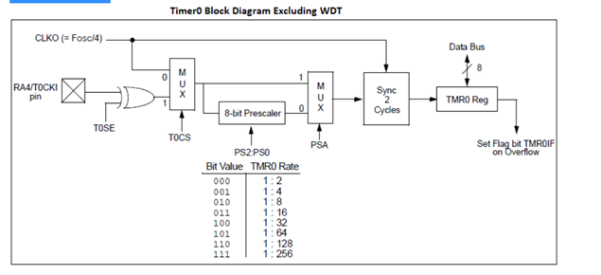
Figure 9. Timer 0 Block Diagram
Steps:
- Calculate the Timer Count for the required delay.
- Set the Presaclar bits in OPTION_REG as per the delay calculations.
- Clear the PSA bit for using the prescalar.
- Select the Clock Source Internal/External using TOCS bit.
- Load the timer value into TMRO register.
- Enable the Timer0 Interrupt by setting TMR0IE bit
- Enable the Global and Peripheral interrupts by setting GIE and PIE bits
#include<pic16f877a.h>
Char value = 0;
#define SBIT_PS2 2
Void interrupt timer_isr()
{
If(TMR0IF==1)
{
Value=~value; // complement the value for blinking the LEDs
TMR0 = 101; /*Load the timer Value, (Note: Timervalue is 101 instaed of 100 as the
TImer0 needs two instruction Cycles to start incrementing TMR0 */
TMR0IF=0; // Clear timer interrupt flag
}
}
Void main()
{
TRISD=0x00; //COnfigure PORTD as output to blink the LEDs
OPTION_REG = (1<<SBIT_PS2); // Timer0 with external freq and 32 as prescalar
TMR0=100; // Load the time value for 1ms delay
TMR0IE=1; //Enable timer interrupt bit in PIE1 register
GIE=1; //Enable Global Interrupt
PEIE=1; //Enable the Peripheral Interrupt
While(1)
{
PORTD = value;
}
}
Output:
Timer 1
The timer TMR1 module is a 16-bit timer/counter with the following features:
- 16-bit timer/counter with two 8-Bit register TMR1H/TMR1L
- Readable and writable
- Software programmable prescaler upto 1:8
- Internal or external clock select
- Interrupt on overflow from FFFFh to 00h
- Edge selects for external clock.
Timer1 register
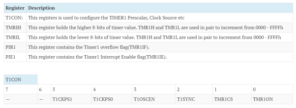
T1CKPS1: T1CKPS0: Timer1 Input Clock Prescale Select bits
11 = 1:8 prescale value
10 = 1:4 prescale value
01 = 1:2 prescale value
00 = 1:1 prescale value
T1OSCEN: Timer1 Oscillator Enable Control bit
1-Oscillator is enabled
0-Oscillator is shut-off
T1SYNC: Timer1 External Clock Input Synchronization Control bit
1-Do not synchronize external clock input
0-Synchronize external clock input
TMR1CS: Timer1 Clock Source Select bit
1-External clock from pin RC0/T1OSO/T1CKI (on the rising edge)
0-Internal clock (FOSC/4)
TMR1ON: Timer1 On bit
1-Enables Timer1
0-Stops Timer1
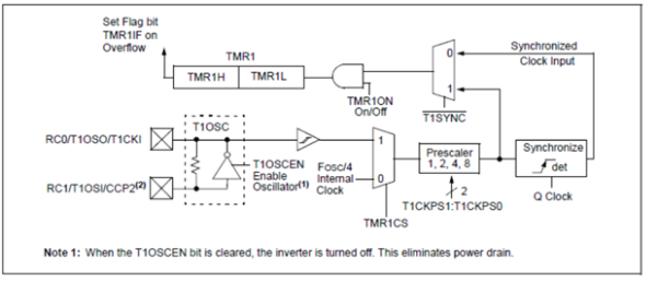
Figure 10. Timer 1 Block Diagram
Steps:
• Calculate the Timer Count for the required delay.
• Set the Presaclar bits in T1CON as per the delay calculations.
• Select the Clock Source Internal/External using TMR1CS bit.
• Load the timer value into TMR1H, TMR1L register.
• Enable the Timer1 Interrupt by setting TMRIE bit
• Enable the Global and Peripheral interrupts by setting GIE and PIE bits
• Finally start the timer by setting TMR1ON bit
#include<pic16f877a.h>
Char value = 0;
#define SBIT_PS1 5
#define SBIT_PS0 4
Void interrupt timer_isr()
{
If(TMR1IF==1)
{
Value=~value; // complement the value for blinking the LEDs
TMR1H=0x0B; // Load the time value(0xBDC) for 100ms delay
TMR1L=0xDC;
TMR1IF=0; // Clear timer interrupt flag
}
}
Void main()
{
TRISD=0x00; //COnfigure PORTD as output to blink the LEDs
T1CON = (1<<SBIT_PS1) | (1<<SBIT_PS0); // Timer0 with external freq and 8 as prescalar
TMR1H=0x0B; // Load the time value(0xBDC) for 100ms delay
TMR1L=0xDC;
TMR1IE=1; //Enable timer interrupt bit in PIE1 register
GIE=1; //Enable Global Interrupt
PEIE=1; //Enable the Peripheral Interrupt
TMR1ON = 1; //Start Timer1
While(1)
{
PORTD = value;
}
}
Timer 2
The TImer2 module is an 8-bit timer/counter with the following features:
- 8-bit timer/counter
- Readable and writable
- Software programmable prescaler/PostScaler upto 1:16
- Interrupt on overflow from FFh to 00h
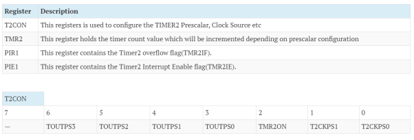
TOUTPS3:TOUTPS0: Timer2 Output Postscale Select bits
0000 = 1:1 postscale
0001 = 1:2 postscale
0010 = 1:3 postscale
•
•
•
1111 = 1:16 postscale
TMR2ON: Timer2 On bit
1-Timer2 is on
0-Timer2 is off
T2CKPS1:T2CKPS0: Timer2 Clock Prescale Select bits
00 = Prescaler is 1
01 = Prescaler is 4
1x = Prescaler is 16
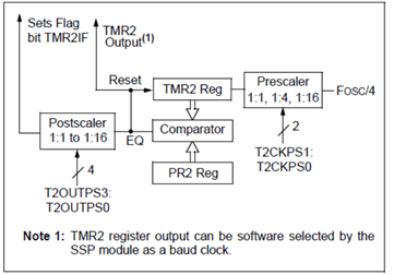
Figure 11. Timer 2 Block Diagram
- Calculate the Timer Count for the required delay.
- Set the Prescaler bits in T2CON as per the delay calculations.
- Load the timer value into TMR2 register.
- Enable the Timer2 Interrupt by setting TMR2IE bit
- Enable the Global and Peripheral interrupts by setting GIE and PIE bits
- Finally start the Timer2 by setting TMR2ON bit
#include<pic16f877a.h>
#define SBIT_T2CKPS1 1
Char value = 0;
Int count = 0;
Void interrupt timer_isr()
{
If(TMR2IF==1)
{
TMR2 = 101; /*Load the timer Value, (Note: Timervalue is 101 instead of 100 as the
Timer2 needs two instruction Cycles to start incrementing TMR2 */
TMR2IF=0; // Clear timer interrupt flag
If(count>=2000) //500us * 2000=1000000us=1sec
{
Count=0;
Value=~value; // complement the value for blinking the LEDs
}
Else
{
Count++; // Keep incrementing the count till it reaches 2000 to generate 1sec delay
}
}
}
Void main()
{
TRISD=0x00; //COnfigure PORTD as output to blink the LEDs
T2CON = (1<<SBIT_T2CKPS1); // Timer2 with external freq and 16 as prescalar
TMR2=100; // Load the timer value for 500us delay
TMR2IE=1; //Enable timer interrupt bit in PIE1 register
GIE=1; //Enable Global Interrupt
PEIE=1; //Enable the Peripheral Interrupt
TMR2ON = 1;
While(1)
{
PORTD = value;
}
}
Interrupts
Interrupts are the signals which alter the flow of an executing program by causing the microcontroller to jump to Interrupt Service Routine to serve the interrupt. These interrupts are given to the microcontroller unit through external pins of the microcontroller.
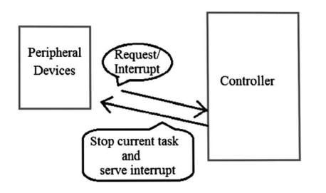
Figure 12. External Interrupts
- Once the controller completes the routine, it returns to the location from where it had made a jump.
- In case interrupts are not used, the program has to constantly poll the input signals and monitor external events for catching the pulses when they occur. In some cases, the program can miss an event. E.g., An infrared slot sensor trying to catch a coin drop. By using an interrupt can the microcontroller can be free to get some other work done by not missing the input. In such cases, external interrupts are used.

INTEDG0: External Interrupt 0 Edge select bit
1= Interrupt on Rising Edge
0= Interrupt on Falling Edge
INTEDG1: External Interrupt 1 Edge select bit
1= Interrupt on Rising Edge
0= Interrupt on Falling Edge
INTEDG2: External Interrupt 2 Edge select bit
1= Interrupt on Rising Edge
0= Interrupt on Falling Edge
RBPU: PORTB Pull-up enable bit
- PORTB has weak internal pull-up. So, to enable them RBPU bit is used.
1= All PORTB Pull-ups are disabled
0= All PORTB Pull-ups are enabled
TMR0IP: TMR0 overflow interrupt Priority
1= High Priority
0= Low Priority
RBIP: RB PORT change Interrupt Priority
1 = High Priority
0 = Low Priority
Steps for Programming
- Set PORTB External interrupt pin as an input.
- Also, make PORTB pins as digital input as it is multiplexed with ADC channels. This is done by disabling ADON bit in the ADCON1 register or by making PBADEN configuration bit low.
- Configure INTCON2 register for edge trigger i.e., positive or negative edge.
- Enable external interrupt (INT0, INT1, INT2) by setting a respective interrupt enable bit in INTCON register.
- Enable Global Interrupt (GIE).
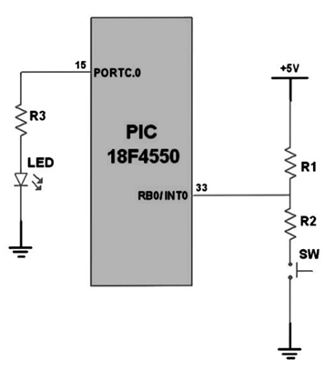
Figure 12. LED Toggling using PIC18F4550 External Interrupt
- Here, the external interrupt event arises from the switch connected to pin PORTB.0 (INT0). This event is negative edge triggered. When the switch is pressed, a low pulse is generated on the INT0 pin. It generates an interrupt as the INTCON2 register is configured to detect negative edge trigger (high to low pulse).
- The control will move to ISR in which LED on PORTC.0 will toggle and the control will move to the main program.
- So, there is no need to poll the PORTB.0 pin continuously.
#include "osc.h"
#include <p18f4550.h>
#define LED LATC
Void External_Interrupt_Init();
Void MSdelay(unsigned int);
Void main()
{
OSCCON=0x72; /* Set internal oscillator to 8MHz*/
TRISC0=0; /* Make PORTC.0 as output*/
LED=0;
External_Interrupt_Init(); /* Initialize External Interrupt*/
While(1);
}
Void External_Interrupt_Init()
{
TRISBbits.TRISB0=1; /* Make INT0 pin as an input pin*/
/* Also make PBADEN off in Configuration file or
Clear ADON in ADCON0 so as to set analog pin as digital*/
INTCON2=0x00; /* Set Interrupt on falling Edge*/
INTCONbits.INT0IF=0; /* Clear INT0IF flag*/
INTCONbits.INT0IE=1; /* Enable INT0 external interrupt*/
INTCONbits.GIE=1; /* Enable Global Interrupt*/
}
Void interrupt ISR()
{
LED = ~(LED); /* Toggle LED on interrupt*/
MSdelay(200);
INTCONbits.INT0IF=0;
}
Void MSdelay(unsigned int val)
{
Unsigned int i,j;
For (i=0; i<val; i++)
For (j=0; j<165; j++); /* Delay count for 1ms for 8MHz freq. */
}
Key takeaway
Timer 0
The TMR0 module is an 8-bit timer/counter with the following features:
- 8-bit timer/counter
- Readable and writable
- 8-bit software programmable prescaler
- Internal or external clock select
- Interrupt on overflow from FFH to 00H
- Edge selects for external clock
Interrupts are the signals which alter the flow of an executing program by causing the microcontroller to jump to Interrupt Service Routine to serve the interrupt. These interrupts are given to the microcontroller unit through external pins of the microcontroller.
Each of the CCP modules contains 16-bit register which operate as:
- 16-bit capture register
- 16-bit compare register
- PWM duty cycle register
Modes of Operation:
Capture:
In Capture mode, the CCP module captures the 16-Bit value of Timer1 module in the CCPRx register for specific user-defined event. When Timer1 module is running timer-mode or synchronized counter-mode.
Compare:
In Compare mode, the 16-Bit value of the CCPRx register is constantly compared against the TMR1 register’s value until a match is found. If found then, the CCPx pin is driven high, or low or not changed by how the programmer defines.
PWM:
In PWM mode, the Timer2 module is used to produce PWM output signal on the CCPx pins (RC2, RC3 respectively). The programmers are responsible for setting the output frequency of PWM signal as well as its duty cycle. The PWM signal is being used for motor speed control, LED dimming, solar chargers and so on.
Capture Mode:
I- CCP Pin Configuration:
In Capture mode, RC2/CCP1 pin is configured as an input by setting the TRISC2 bit. If RC2/CCP1 pin is configured as output, a write to the port can cause Capture condition.
II- Timer1 Mode Selection:
To use capture feature Timer1 must be running in Timer mode, or Synchronized Counter mode. In Asynchronous Counter mode, the capture operation does not work.
III- Software Interrupt:
When the Capture mode is changed, it generates false capture interrupt. The user should keep bit CCP1IE clear in order to avoid false interrupts and clear the flag bit, CCP1IF for any change in operating mode.
IV- CCP Pre-scaler Setting:
There are four prescaler settings, specified by bits CCP1M3:CCP1M0. Switching from one capture prescaler to another generates an interrupt.
Step1 – Setup Timer1 for Timer or Counter Mode
[ For Timer Mode]
// -- [[ Configure Timer1 to Operate in Timer Mode]] --
// Clear The Timer1 Register. To start counting from 0
TMR1 = 0;
// Choose the local clock source (timer mode)
TMR1CS = 0;
// Choose the desired prescaler ratio (1:1)
T1CKPS0 = 0;
T1CKPS1 = 0;
[ For Counter Mode]
//--[ Configure The Timer1 Module to Operate in Counter Mode]--
TMR1 = 0;
// Choose the desired prescaler ratio (1:1)
T1CKPS0 = 0;
T1CKPS1 = 0;
// Choose the external clock source (counter mode)
TMR1CS = 1;
T1OSCEN = 1;
// Enable Synchronization for Counter Mode
T1SYNC = 0;
//--[ Configure The Timer1 Module to Operate in Counter Mode]--
TMR1 = 0;
// Choose the desired prescaler ratio (1:1)
T1CKPS0 = 0;
T1CKPS1 = 0;
// Choose the external clock source (counter mode)
Step 2 – Turn ON Timer1
TMR1ON = 1;
1
TMR1ON = 1;
Step 3,4 – Setup CCP1 For Capture Mode & Choose Event
//--[ Configure The CCP1 Module to Operate in Capture Mode]--
CCP1M0 = x;
CCP1M1 = x;
CCP1M2 = x;
CCP1M3 = x;
Replace x’s with the proper bit-pattern for the capture mode with the event you wish to select.
Step 5 – Configure the CCP1 Interrupt
// Enable CCP1 Interrupt
CCP1IE = 1;
PEIE = 1;
GIE = 1;
Step 6 – Write the ISR Handler For CCP-Capture Interrupt
Void interrupt ISR()
{
If (CCP1IF)
{
// Do Some Stuff...
}
}
Compare:
In Compare Mode, the 16-Bit CCPR1 (CCPR1H:CCPR1L) register is constantly compared against the TMR1 register. When a match occurs, The CCP1 pin (RC2) is:
- Driven Low
- Driven High
- Remains Unchanged
I- CCP Pin Configuration:
The user must configure the RC2/CCP1 pin as an output by clearing TRISC2 bit. Clearing the CCP1CON register will force RC2/CCP1 compare output latch to the default low level. This is not the PORTC I/O data latch.
II- Timer1 mode selection:
Timer1 runs in Timer mode or Synchronized Counter mode, if the CCP module uses compare feature. In Asynchronous Counter mode, the compare operation will not work.
III- Software Interrupt Mode:
When Generate Software Interrupt mode is chosen, the CCP1 pin does not affect. The CCPIF bit is set, causing a CCP interrupt (if enabled).
IV- Special Event Trigger:
In this mode, an internal hardware trigger is generated to initiate an action. The special event trigger output of CCP1 resets TMR1 register pair. This allows CCPR1 register to effectively be a 16-bit programmable period register for Timer1. The special event trigger output of CCP2 resets the TMR1 register pair and starts A/D conversion.
Step 1 – Setup Timer1 for Timer or Counter Mode
[ For Timer Mode]
// -- [[ Configure Timer1 to Operate in Timer Mode]] --
// Clear The Timer1 Register. To start counting from 0
TMR1 = 0;
// Choose the local clock source (timer mode)
TMR1CS = 0;
// Choose the desired prescaler ratio (1:1)
T1CKPS0 = 0;
T1CKPS1 = 0;
[ For Counter Mode]
//--[ Configure The Timer1 Module to Operate in Counter Mode]--
TMR1 = 0;
// Choose the desired prescaler ratio (1:1)
T1CKPS0 = 0;
T1CKPS1 = 0;
// Choose the external clock source (counter mode)
TMR1CS = 1;
T1OSCEN = 1;
// Enable Synchronization for Counter Mode
T1SYNC = 0;
Step 2 – Turn ON Timer1
TMR1ON = 1;
1
Step 3 – Preload the CCPR1 Register
CCPR1 = N;
Where N is the value that we get from the calculations
Step 4,5 – Setup CCP1 For Compare Mode & Choose Event
//--[ Configure The CCP1 Module to Operate in Compare Mode]--
CCP1M0 = x;
CCP1M1 = x;
CCP1M2 = x;
CCP1M3 = x;
Replace x‘s with the proper bit-pattern for the compare mode with the event you wish to select.
Step 6 – Configure the CCP1 Interrupt
// Enable CCP1 Interrupt
CCP1IE = 1;
PEIE = 1;
GIE = 1;
Step 7 – Write the ISR Handler For CCP-Compare Interrupt
Void interrupt ISR()
{
If (CCP1IF)
{
// Do Some Stuff...
}
}
Program:
#include <xc.h>
#include "config.h"
#include <stdint.h>
Uint8_t X=0; // Counter for Compare Match Events
Void main(void)
{
//--[ Configure The IO Ports]--
// Set The Output Pin for the LED
TRISC4=0;
RC4=0; // Initially OFF
//--[ Configure The Timer1 Module to Operate in Timer Mode]--
TMR1 = 0;
T1CKPS0 = 0;
T1CKPS1 = 0;
TMR1CS = 0;
TMR1ON = 1;
//--[ Configure The CCP1 Module to Operate in Compare Mode]--
// Preload The CCPR1 Register
CCPR1 = 50000;
// CCP in Compare Mode, CCPx Pin Is Unchanged & Trigger Special Event
CCP1M0 = 1;
CCP1M1 = 1;
CCP1M2 = 0;
CCP1M3 = 1;
// Enable CCP1 Interrupt
CCP1IE = 1;
PEIE = 1;
GIE = 1;
// Create The Main Loop of The System
While (1)
{
// Stay Idle, everything is taken care of in the ISR
}
Return;
}
// Write The ISR Handler
Void interrupt ISR()
{
If (CCP1IF)
{
X++;
If (X==10)
{
// Toggle The LED
RC4 = ~RC4;
X = 0;
}
// Clear The Interrupt Flag Bit
CCP1IF = 0;
}
}
PWM generation
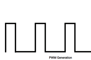
Figure 13. PWM generation

A pulse with a period of 10ms will remain ON (high) for 2ms.Therefore, duty cycle will be
D = 2ms / 10ms = 20%
CCPR1H and CCPR1L register
In CCP module, there is a 16-bit register which is split as two 8-bit registers – CCPR1H and CCPR1L.

Only CCPR1L is used to decide the duty cycle of the PWM. CCPR1H is not user accessible for the PWM mode.
- As the PIC18F4550 generates a 10-bit PWM pulse, to set the duty cycle it uses 10-bit register. The higher 8 bits (MSBs) DC1B9: DC1B2 of this register are in CCPR1L register (8-bit) and lower 2 bits (LSBs) DC1B1: DC1B0, which are used for a decimal portion in duty cycle, are in CCP1CON register at bit 5 and 4 respectively.
- So, the 10-bit value for duty cycle is represented by CCPR1L: CCP1CON<5: 4>
PR2 register
- It is an 8-bit register which is used to load a count for a period of the pulse (TPWM).
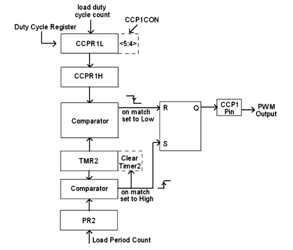
Figure 14. Working
- Load the period value in a PR2 register and the duty cycle value in CCPR1L: CCP1CON<5: 4> registers and initialize CCP1 pin as an output.
- Configure T2CON register and set the TMR2 register to 0. Also, start the Timer2.
- Now when a match occurs between registers PR2 and TMR2, pin CCP1 is pulled high and TMR2 is cleared.
- The value of CCPR1L along with the CCP1CON<5: 4> which is a count for duty cycle is moved to the CCPR1H.
- Finally, TMR2 is compared with the CCPR1H along with two lower bits of a duty cycle. When matched, the pin CCP1goes low.

Steps:
- Load the PR2 value which will decide the period of the pulse.
- Set the duty cycle by loading a value in the CCPR1L: CCP1CON<5: 4>
- Configure the CCP1CON register for setting a PWM mode.
- Initialize the pin CCP1as an output pin which will give PWM output.
- Configure the T2CON register and enable TMR2 using T2CON
#include "osc_config.h"
#include <pic18f4550.h>
Void main()
{
OSCCON = 0x72; /* Set internal clock to 8MHz */
TRISC2 = 0; /* Set CCP1 pin as output for PWM out */
PR2 = 199; /* Load period value */
CCPR1L = 40; /* load duty cycle value */
T2CON = 0; /* No pre-scalar, timer2 is off */
CCP1CON = 0x0C; /* Set PWM mode and no decimal for PWM */
TMR2 = 0; /* Clear Timer2 initially */
TMR2ON = 1; /* Timer ON for start counting*/
While(1);
}
Key takeaway
Each of the CCP modules contains 16-bit register which operate as :
- 16-bit capture register
- 16-bit compare register
- PWM duty cycle register
DC motor normally works in 6-12v, 300mA and it has other drawbacks like the back EMF produced by the DC motor may harm the controller ports and damage them. The solution to the above problems is using motor driving circuit usually known as H-Bridges. They are basically built using FETs and many dedicated ICs are also available like L293D etc.
These are dual H-bridge motor drivers that is by using one IC we can control two DC motors in both clockwise and counter clockwise directions. The L293D can provide bidirectional drive currents of up to 600mA at voltages from 4.5 V to 36 V.
The below circuit shows interfacing L293D with PIC microcontroller to control a DC motor.
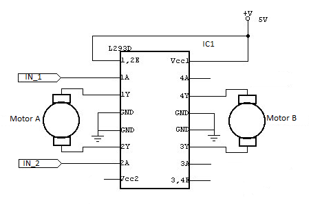
Figure 15. DC motor circuit
In both ICs, drivers are enabled in pairs with drivers 1 and 2 are enabled by a high input to 1,2 EN and drivers 3 and 4 are enabled by a high input to 3,4 EN. When drivers are enabled, their outputs will be active and in phase with their inputs. When drivers are disabled, their outputs will be off and will be in the high-impedance state.
For example, we use 20MHz clock and the o/p frequency is 2KHz;
Whereas PWM period = 1/frequency (that will be 1/2000 = .0005)
.0005 = [PR2 + 1] • [1 / 20000000] • 16
PR2 + 1 = [.0005 • 20000000] / 16
PR2 + 1 = 625
PR2 = 624
PR2 = 0x270 (624 in hex)
Program:
Void main()
{
Short duty = 0; //initial value for duty
TRISD = 0xFF; //PORTD as input
TRISC = 0x00; //PORTC as output
TRISB = 0x00; //PORTB as output
PORTB = 0x02; //Run motor in anticlock wise
PWM1_Init(1000); //Initialize PWM1
PWM1_Start(); //start PWM1
PWM1_Set_Duty(duty); //Set current duty for PWM1
While (1) // endless loop
{
If (!RD0_bit && duty<260) //if button on RD0 pressed
{
Delay_ms(40);
Duty = duty + 10; //increment current_duty
PWM1_Set_Duty(duty); //Change the duty cycle
}
If (!RD1_bit && duty >0) //button on RD1 pressed
{
Delay_ms(40);
Duty = duty - 10; //decrement duty
PWM1_Set_Duty(duty);
}
Delay_ms(10); // slow down change pace a little
}
}
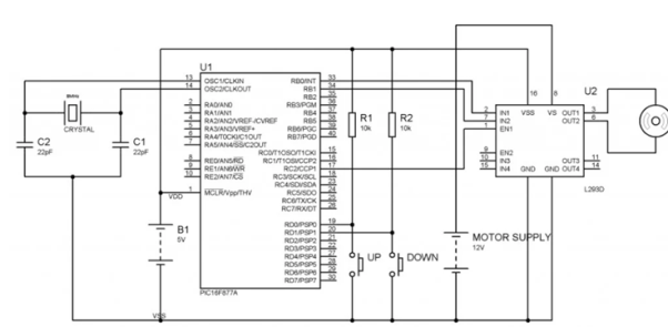
Figure 16. Interfacing DC motor with PIC
Key takeaway
DC motor normally works in 6-12v, 300mA and it has other drawbacks like the back EMF produced by the DC motor may harm the controller ports and damage them. The solution to the above problems is using motor driving circuit usually known as H-Bridges.
The PIC 18F4321 contains an on‑chip A/D converter (or sometimes called ADC) module with 13 channels (AN0-AN12). An analog input can be selected as an input on one of these 13 channels, and can be converted to a corresponding 10‑bit digital number. Three control registers, namely, ADCON0 through ADCON2, are used to perform the conversion. The ADCON0 register, shown in Figure below, controls the operation of the A/D module. The ADCON0 register can be programmed to select one of 13 channels using bits CHS3 through CHS0 (bits 5 through 2). The conversion can be started by setting the GO/ DONE (bit 1) to 1. Once the conversion is completed, this bit is automatically cleared to 0 by the PIC18F4321. The ADCON1 register, shown in Figure below, configures the functions of the port pins as Analog (A) input or Digital (D) I/O.

Bit 7-6 Unimplemented: Read as ‘0’
Bit 5-2 CHS3:CHS0: Analog Channel Select
Bits 0000 = Channel 0 (AN0)
0001 = Channel 1 (AN1)
0010 = Channel 2 (AN2)
0011 = Channel 3 (AN3)
0100 = Channel 4 (AN4)
0101 = Channel 5 (AN5)
0110 = Channel 6 (AN6)
0111 = Channel 7 (AN7)
1000 = Channel 8 (AN8)
1001 = Channel 9 (AN9)
1010 = Channel 10 (AN10)
1011 = Channel 11 (AN11)
1100 = Channel 12 (AN12)
1101 = Unimplemented
1110 = Unimplemented
1111 = Unimplemented
Bit 1 GO/ DONE: A/D Conversion Status bit
When GO/DONE = 1:
1 = A/D conversion in progress
0 = A/D idle
Bit 0 ADON: A/D On bit
1 = A/D converter module is enabled
0 = A/D converter module is disabled
Figure 17 ADCON0 (A/D Control Register0)
The table shown in Figure below shows how the port bits are defined as analog or digital signals by programming the PCFG3 through PCFG0 bits (bits 3 through 0) of the ADCON1 register. This register can also be

Bit 7 ADFM: A/D Result Format Select bit
1 = Right justified; 10-bits in lower 2 bits of ADRESH with upper 6 bits as 0’s and in 8 bits of ADRESL
0 = Left justified; 8-bit result in ADRESH and the contents of ADRESL are ignored. Used for 8-bit conversion.
Bit 6 Unimplemented: Read as ‘0’
Bit 5-3 ACQT2:ACQT0: A/D Acquisition Time Select bits
111 = 20 TAD
110 = 16 TAD
101 = 12 TAD
100 = 8 TAD
011 = 6 TAD
010 = 4 TAD
001 = 2 TAD
000 = 0 TAD (1)
Bit 2-0 ADCS2:ADCS0: A/D Conversion Clock Select bits
111 = FRC (clock derived from A/D RC oscillator) (1)
110 = FOSC/64
101 = FOSC/16
100 = FOSC/4
011 = FRC (clock derived from A/D RC oscillator) (1)
010 = FOSC/32
001 = FOSC/8
000 = FOSC/2
Figure 18 ADCON2 (A/D Control Register 2)
The following steps should be followed to perform an A/D conversion:
Configure the A/D module
- Configure analog pins, voltage reference, and digital I/O (ADCON1)
- Select A/D input channel (ADCON0)
- Select A/D acquisition time (ADCON2)
- Select A/D conversion clock (ADCON2) • Turn on A/D module (ADCON0)
Configure A/D interrupt (if desired)
- Clear ADIF bit (bit 6 of PIR1)
- Set ADIE bit
- Set GIE bit (bit 7) and PEIE (bit 6) of INTCON register
- All interrupts including A/D Converter interrupt, branch to address 0x000008 (default) upon power‑on reset. However, the A/D Converter interrupt can be configured as low priority by setting the ADIP bit (bit 6) of the IPRI register to branch to address 0x000018. The instruction, BSF IPR1, ADIP can be used for this purpose.
Wait for the required acquisition time (if required).
Start conversion:
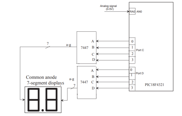
Figure 18 Interfacing of on-chip ADC
Example
A PIC18F4321 microcontroller shown in Figure above is used to implement a voltmeter to measure voltage in the range 0 to 5 V and display the result in two decimal digits: one integer part and one fractional part. Using polled I/O, write a PIC18F assemble language program to accomplish this.
In order to design the voltmeter, the PIC18F4321 on‑chip A/D converter will be used. Three registers, ADCON0‑ADCON2, need to be configured. In ADCON0, bit 0 of PORT A (RA0/AN0) is designated as the analog signal to be converted. Hence, CHS3CHS0 bits (bits 5-2) are programmed as 0000 to select channel 0 (AN0). The ADCON0 register is also used to enable the A/D, start the A/D, and then check the “end of conversion” bit.
In the PIC18F assembly language program provided below, the ADCON0 is loaded with 0x01 which will select AN0, and enable A/D. The reference voltages are chosen by programming the ADCON1 register. In this example, VDD (by clearing bit 4 of ADCON1 to 0), and VSS (by clearing bit 5 of ADCON1 to 0) will be used. Note that VDD and VSS are already connected to the PIC18F4321. The ADCON1 register is also used to configure AN0 (bit 0 of Port A) as an analog input by writing 1101 at PCFG3‑PCFG0 (bits 3‑0 of ADCON1).
Note that there are several choices to configure AN0 as an analog input. In the program, the ADCON1 is loaded with 0x0D which will select VSS and VDD as reference voltage sources, and AN0 as analog input. In the program, the ADCON2 is loaded with 0x29 which will provide the 8‑bit result left justified (when 8 bits are obtained from 10 bits, the Lower two bits in ADRESL are discarded), select 12 TAD (requires at least 11 TAD for 10‑bit conversion), and select Fosc/8.
The ADCON2 is used to set up the acquisition time, conversion clock, and, also, if the result is to be left or right justified. In this example, 8‑bit result is assumed. The A/D result is configured as left justified, and, therefore, the 8‑bit register ADRESH will contain the result. The contents of ADRESL are ignored. Note that the maximum decimal value that can be accommodated in 8 bits of
ADRESH is 25510 (FF16). Hence, the maximum voltage of 5 V will be equivalent to 25510.
This means that 1 volt = 51 (decimal).
The display (D) in decimal is given by
D = 5 × (input/255) = input/51 = Integer part quotient + remainder
This gives the integer part. The fractional part in decimal is
F = (remainder/51) ×10= (remainder)/5
For example, suppose that the decimal equivalent of the 8‑bit output of A/D is 200.
D = 200/51 =quotient = 3, remainder = 47
Integer part = 3,
Fractional part, F = 47/5 = 9
Therefore, the display will show 3.9 V. From these equations, the final result will be in BCD. Both integer and fractional parts of the result will be output to two 7447s (BCD to seven‑segment decoder) in order to display them on two seven‑segment displays arranged in a row.
Key takeaway
The PIC 18F4321 contains an on‑chip A/D converter (or sometimes called ADC) module with 13 channels (AN0-AN12). An analog input can be selected as an input on one of these 13 channels, and can be converted to a corresponding 10‑bit digital number. Three control registers, namely, ADCON0 through ADCON2, are used to perform the conversion.
In case of temperature the Celsius and Fahrenheit scale thermometer displays the ambient temperature through LCD display.
This consists of two sections:
- One senses the temperature. The temperature sensor is LM 35.
- The other converts the temperature value into a suitable number in Celsius scale by ADC0804.
The temperature is sensed in Celsius scale and converted into Fahrenheit scale temperature by using Celsius to Fahrenheit conversion formulae.
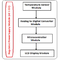
Figure 19: Process
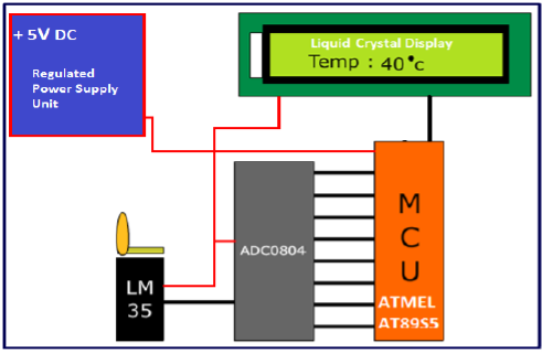
Figure 20. Circuit Diagram
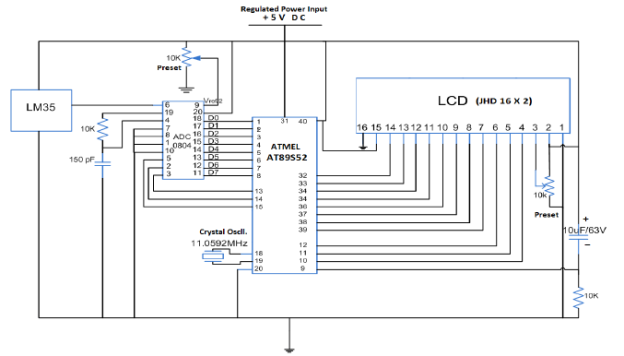
Figure 21. Interfacing of Temperature sensor with microcontroller
- The temperature sensor used is LM35. The LM 35 IC generates a 10mV variation in its output voltage for every degree Celsius change in temperature. The output of the temperature sensor is analog in nature.
- Hence, there is a need for analog to digital convertor to convert the analog input to its equivalent binary output.
- The ADC 0804 is the analog to digital convertor IC. It is a single channel converter that converts the analog input up to a range of 5V into its equivalent 8-bit binary output.
- The step size is defined by the voltage applied at Vref/2 pin of the ADC IC.
For example, if the voltage at Vref/2 pin is set to 1.28V then ADC step size will be 10 mV. Similarly, if the input voltage is 1V the equivalent binary output of ADC will be 1000 or 0110, 0100 in binary.
- For every 10mV rise of input voltage the 8-bit binary output of ADC is incremented by one. Different step size can be selected by changing the voltage input to Vref/2 pin.
- The step size of ADC is calibrated by using a preset to match to actual temperature.
- Once ADC is calibrated it provides the correct output.
- The binary output of ADC is fed parallel to the port of the microcontroller. The microcontroller reads the input through ADC and displays its corresponding decimal value on LCD which indicates temperature.
Program:
ORG 00H
MOV P1,#11111111B // initializes P1 as input port
MOV P0,#00000000B // initializes P0 as output port
MOV P3,#00000000B // initializes P3 as output port
MOV DPTR,#LABEL // loads the address of "LABEL" to DPTR
MAIN: MOV R4,#250D // loads register R4 with 250D
CLR P3.7 // makes Cs=0
SETB P3.6 // makes RD high
CLR P3.5 // makes WR low
SETB P3.5 // low to high pulse to WR for starting conversion
WAIT: JB P3.4,WAIT // polls until INTR=0
CLR P3.7 // ensures CS=0
CLR P3.6 // high to low pulse to RD for reading the data from ADC
MOV A,P1 // moves the digital output of ADC to accumulator A
MOV B,#10D // load B with 10D
DIV AB // divides the content of A with that in B
MOV R6,A // moves the quotient to R6
MOV R7,B // moves the remainder to R7
DLOOP:SETB P3.2 // sets P3.2 which activates LED segment 1
MOV A,R6 // moves the quotient to A
ACALL DISPLAY // calls DISPLAY subroutine
MOV P0,A // moves the content of A to P0
ACALL DELAY // calls the DELAY subroutine
CLR A // clears A
MOV A,R7 // moves the remainder to A
CLR P3.2 // deactivates LED segment 1
SETB P3.1 // activates LED segment 2
ACALL DISPLAY
MOV P0,A
ACALL DELAY
CLR A
CLR P3.1 // deactivates LED segment 2
DJNZ R4,DLOOP // repeats the loop "DLOOP" until R4=0
SJMP MAIN // jumps back to the main loop
DELAY: MOV R3,#255D // produces around 0.8mS delay
LABEL1: DJNZ R3,LABEL1
RET
DISPLAY: MOVC A,@A+DPTR // converts A's content to corresponding digit drive pattern
RET
LABEL: DB 3FH // LUT (look up table) starts here
DB 06H
DB 5BH
DB 4FH
DB 66H
DB 6DH
DB 7DH
DB 07H
DB 7FH
DB 6FH
END
References:
1. Kenneth J. Ayala, ‘The 8051 Microcontroller Architecture, Programming and Applications’, Cengage Learning, 3rd Edition
2. Ajay Deshmukh, “Microcontrollers Theory and Applications”, TATA McGraw Hill, 4th Edition
3. Peatman, John B, “Design with PIC Microcontroller”, Pearson Education PTE, 1st Edition
4. Data Sheet of PIC 18Fxxxx series