Unit - 5
Real Word Interfacing With 18FXXXX
Five ports are selected depending on the device and features selected. When a peripheral is enabled, the pin is not used as general purpose I/O pin.
Each port has three registers for its operation:
- TRIS registers (Data Direction register)
- PORT register (reads the levels on the pins of the device)
- LAT register (Data Latch register)
The data latch is used for read-modify write operations depending on the value of I/O pins.
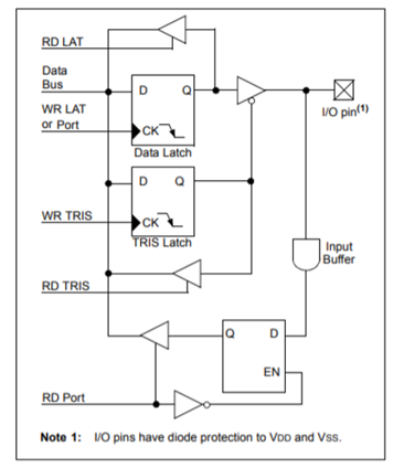
Figure 1. Port Operation
The TRISA register controls PORTA pins direction while being used as analog inputs. The user must ensure that the bits in TRISA register are set when using them as analog inputs.
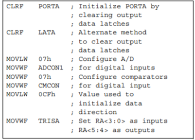
Fig 2 Program for initializing port A
PORTB is an 8-bit wide, bidirectional port. The Data Direction register is TRISB. When TRISB bit (= 1) then PORTB pin serves as input. Clearing a TRISB bit (= 0) PORTB pin serves as output. The Data Latch register (LATB) is memory mapped. Read-modify-write operations on LATB register read and write the latched output value for PORTB
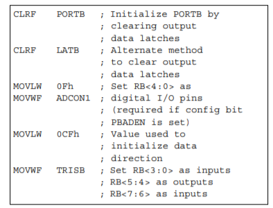
Fig 3 Program for initializing Port B
PORTC is an 8-bit wide, bidirectional port. The Data Direction register is TRISC. Setting a TRISC bit (= 1) will make PORTC pin an input. Clearing a TRISC bit (= 0) will make the PORTC pin an output. The Data Latch register (LATC) is memory mapped. Read-modify-write operations on LATC register read and write the latched output value for PORTC. When enabling peripheral functions, define TRIS bits for each PORTC pin. Some peripherals override TRIS bit to make the pin an output, while other peripherals override the TRIS bit to make the pin as input.
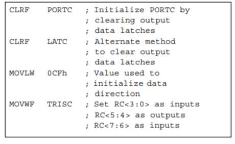
Fig 4 Program for initializing Port C
PORTD is an 8-bit wide, bidirectional port. The corresponding Data Direction register is TRISD. Setting a TRISD bit (= 1) will make the corresponding PORTD pin an input. Clearing a TRISD bit (= 0) will make the corresponding PORTD pin an output. The Data Latch register (LATD) is also memory mapped. Read-modify-write operations on the LATD register read and write the latched output value for PORTD.
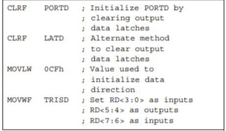
Program for initializing PORT D
The fourth pin of PORTE (MCLR/VPP/RE3) is an input pin. Its operation is controlled by MCLRE configuration bit. When selected as port pin (MCLRE = 0), it functions as digital input pin; Otherwise, it functions as the device’s Master Clear input. In either configuration, RE3 functions as programming voltage input during programming.
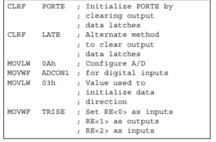
Program for initializing Port E
Key takeaway
Five ports are selected depending on the device and features selected. When a peripheral is enabled, the pin is not used as general purpose I/O pin.
Each port has three registers for its operation:
- TRIS registers (Data Direction register)
- PORT register (reads the levels on the pins of the device)
- LAT register (Data Latch register)
A light-emitting diode (LED) is a two-lead semiconductor light source. It has p–n junction diode that emits light when activated. When suitable voltage is applied to the leads, electrons recombine with electron holes within the device, releasing energy in the form of photons. This effect is called electroluminescence. The color of light is determined by energy band gap of semiconductor.
When operated in a forward biased direction Light Emitting Diodes are semiconductor devices that convert electrical energy into light energy.
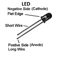
Figure 5. LED
An LED is interfaced with PIC18FXXX microcontroller for various purpose. The Port Pins are configured in output direction. So, is Logic "1" is at the O/P pin, then LED will be turned "ON"if Logic "0" is given the LED will be turned "OFF".
Simply: Logic "1" -> 5V DC to output pin
Logic "0" -> 0 V to output pin.
LED with common cathode mode can be connected with PIC18FXX along with a resistor.
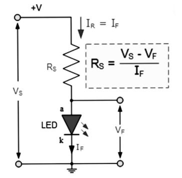
Figure 6. LED with resistor
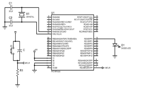
Figure 7. Interfacing Diagram
Program:
#include<p18f4520.h>
Void DELAY();
#pragma config OSC=HS
#pragma config PWRT=OFF
#pragma config WDT=OFF
#pragma config DEBUG=OFF, LVP=OFF
Void main()
{
TRISDbits.RD0 = 0x00; //set RD0 pin direction as an output
While(1) //forever loop
{
PORTDbits.RD0=0X01; //set RD0 pin as HIGH
DELAY(); //call delay
PORTDbits.RD0=0X00; //CLEAR RD0 piN
DELAY(); //call delay
}
}
Void DELAY()
{
Unsigned int i;
For(i=0;i<10000;i++);
}
Key takeaway
A light-emitting diode (LED) is a two-lead semiconductor light source. It has p–n junction diode that emits light when activated. When suitable voltage is applied to the leads, electrons recombine with electron holes within the device, releasing energy in the form of photons.
To interface LCD with PIC microcontroller use GPIO pins because we need to send control and data signals to LCD through these I/O pins.
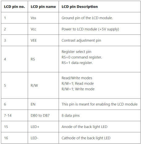
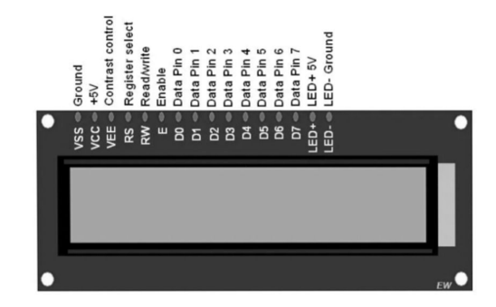
Figure 8. LCD
In 8-bit mode interfacing, use 11 pins of pic microcontroller and in 4-bit mode use 6 GPIO pins.
A variable resistor is used to adjust the contrast of 5×8 dot pixels according to background light.
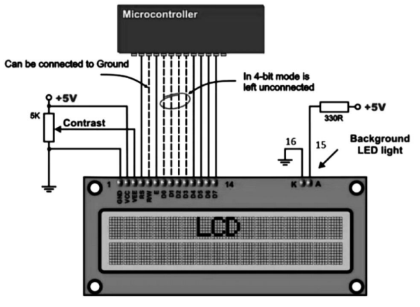
Figure 9. 4/8 -bit mode Interfacing
To interface LCD, follow these steps:
- Define PIC18F4450 pin that we want to use for sending commands and data to LCD
- After that send configuration commands to select mode and other configuration settings
- Oncesuccessfully configured LCD, transmit data to LCD.
Mostly used commands or instructions for LCD
Sr.No | Instruction | Hex |
1 | Function Set: 8-bit mode, 1 Line, 5×7 Dots matrix for each character display | 0×30 |
2 | Function Set: 8-bit mode, 2 Line, 5×7 Dots matrix for each character display | 0×38 |
3 | Function Set: 4-bit mode, 1 Line, 5×7 Dots matrix for each character display | 0×20 |
4 | Function Set: 4-bit mode, 1 Line, 5×7 Dots matrix for each character display | 0×28 |
5 | Clear display screen | 0×01 |
6 | Return Home | 0×02 |
7 | Decrement Cursor (shift to left) | 0×04 |
8 | Decrement Cursor (shift to right) | 0×05 |
9 | Display off Cursor off | 0×08 |
10 | Display on Cursor on | 0×0E |
11 | Display on Cursor off | 0×0C |
12 | Display on cursor blinking | 0×0F |
13 | Shift entire display left | 0×18 |
14 | Shift entire display left | 0×1C |
15 | Move Cursor left by one character | 0×10 |
16 | Move Cursor right by one character | 0×14 |
17 | Clear Display (also clear DDRAM content) | 0×01 |
18 | Force cursor position on first position of first | 0×80 |
19 | Force cursor position on first position of second row | 0×C0 |
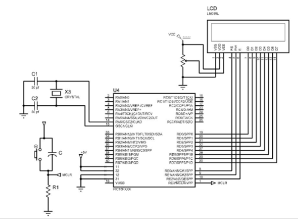
Figure 10. Interfacing LCD
Program:
Write an Embedded C Program to display word "AB " using 8-bit mode
#include<p18f4520.h>
#pragma config OSC=HS
#pragma config PWRT=OFF
#pragma config WDT=OFF
#pragma config DEBUG=OFF, LVP=OFF
Void lcdcmd(unsigned char value);//Function Prototype declaration
Void lcddata(unsigned char value);
Void msdelay(unsigned int itime);
#define ldata PORTD //Declare ldata variable for PORTD
#define rs PORTEbits.RE0 //Declare rs variable for pin RE0
#define rw PORTEbits.RE1 //Declare rw variable for pin RE1
#define en PORTEbits.RE2 //Declare en variable for pin RE2
Void main()
{
TRISD = 0x00; //Set direction of PORTD as output
ADCON1=0X0F;
TRISE=0X00; //set direction of PORTE as output
Msdelay(50);
Lcdcmd(0x38); //16x2 LCD
Msdelay(50);
Lcdcmd(0x0E);
Msdelay(15);
Lcdcmd(0x01); //clear Display screen
Msdelay(15);
Lcdcmd(0x06); //Increment cursor and shift right
Msdelay(15);
Lcdcmd(0x80); //Force cursor on first row first position
Lcddata('S'); //Display character 'S'
Msdelay(50);
Lcddata('K'); //Display character 'K'
Msdelay(50);
}
Void lcdcmd (unsigned char value)
{
Ldata=value; //Send the command value to PORTD
Rs=0; //selection of command register of LCD
Rw=0;
En=1; //Generate High to Low pulse on Enable pin
Msdelay(1);
En=0;
}
Void lcddata (unsigned char value)
{
Ldata=value; //Send the command value to PORTD
Rs=1; //selection of DATA register of LCD
Rw=0;
En=1; //Generate High to Low pulse on Enable pin
Msdelay(1);
En=0;
}
Void msdelay (unsigned int itime)
{
Int i,j;
For(i=0;i<itime;i++)
For(j=0;j<135;j++);
}
Keypad is used as an input device to read the key pressed by user and to process it. 4x4 keypad consists of 4 rows and 4 columns. Switches are placed between the rows and columns. A key press establishes a connection between corresponding row and column between which the switch is placed.
In order to read the key press, we need to configure the rows as outputs and columns as inputs.
Columns are read after applying signals to the rows in order to determine whether a key is pressed or not and if pressed, which key is pressed.
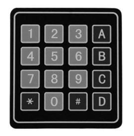
Figure 11. Keyboard matrix.
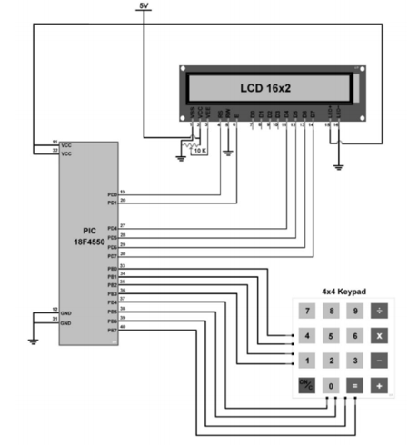
Figure 12. Keyboard Interfacing
#include <pic18f4550.h>
#include "Configuration_Header_File.h"
#include "16x2_LCD_4bit_File.h"
Unsigned char keyfind(); /* function to find pressed key */
#define write_portLATB /* latch register to write data on port */
#define read_portPORTB /* PORT register to read data of port */
#define Direction_Port TRISB
Unsigned char col_loc,rowloc,temp_col;
Unsigned char keypad[4][4]= {'7','8','9','/',
'4','5','6','*',
'1','2','3','-',
' ','0','=','+'};
Void main()
{
Char key;
OSCCON = 0x72;
RBPU=0; /* activate pull-up resistor */
LCD_Init(); /* initialize LCD16x2 in 4-bit mode */
LCD_String_xy(0,0,"Press a Key");
LCD_Command(0xC0); /* display pressed key on 2nd line of LCD */
While(1)
{
Key = keyfind(); /* find a pressed key */
LCD_Char(key); /* display pressed key on LCD16x2 */
}
}
Unsigned char keyfind()
{
Direction_Port = 0xf0; /* PORTD.0-PORTD.3 as a Output Port and PORTD.4-PORTD.7 as a Input Port*/
Unsigned char temp1;
Write_port = 0xf0; /* Make lower nibble as low(Gnd) and Higher nibble as High(Vcc) */
Do
{
Do
{
Col_loc = read_port& 0xf0; /* mask port with f0 and copy it to col_loc variable */
}while(col_loc!=0xf0); /* Check initially at the start there is any key pressed*/
Col_loc = read_port& 0xf0; /* mask port with f0 and copy it to col_loc variable */
}while(col_loc!=0xf0);
MSdelay(50);
Write_port = 0xf0; /* Make lower nibble as low(Gnd) and Higher nibble as High(Vcc) */
Do
{ do
{
Col_loc = read_port& 0xf0;
}while(col_loc==0xf0); /* Wait for key press */
Col_loc = read_port& 0xf0;
}while(col_loc==0xf0); /* Wait for key press */
MSdelay(20);
Col_loc = read_port& 0xf0;
While(1)
{
Write_port = 0xfe; /* make Row0(D0) Gnd and keep other row(D1-D3) high */
Col_loc = read_port& 0xf0; /* Read Status of PORT for finding Row */
Temp_col=col_loc;
If(col_loc!=0xf0)
{
Rowloc=0; /* If condition satisfied get Row no. Of key pressed */
While(temp_col!=0xf0) /* Monitor the status of Port and Wait for key to release */
{
Temp_col = read_port& 0xf0; /* Read Status of PORT for checking key release or not */
}
Break;
}
Write_port = 0xfd; /* make Row1(D1) Gnd and keep other row(D0-D2-D3) high */
Col_loc = read_port& 0xf0; /* Read Status of PORT for finding Row */
Temp_col=col_loc;
If(col_loc!=0xf0)
{
Rowloc=1; /* If condition satisfied get Row no. Of key pressed*/
While(temp_col!=0xf0) /* Monitor the status of Port and Wait for key to release */
{
Temp_col = read_port& 0xf0; /* Read Status of PORT for checking key release or not */
}
Break;
}
Write_port = 0xfb; /* make Row0(D2) Gnd and keep other row(D0-D1-D3) high */
Col_loc = read_port& 0xf0; /* Read Status of PORT for finding Row*/
Temp_col=col_loc;
If(col_loc!=0xf0)
{
Rowloc=2; /* If condition satisfied get Row no. Of key pressed */
While(temp_col!=0xf0) /* Wait for key to release */
{
Temp_col = read_port& 0xf0; /* Read Status of PORT for checking key release or not */
}
Break;
}
Write_port = 0xf7; /* make Row0(D3) Gnd and keep other row(D0-D2) high */
Col_loc = read_port& 0xf0; /* Read Status of PORT for finding Row */
Temp_col=col_loc;
If(col_loc!=0xf0)
{
Rowloc=3; /* If condition satisfied get Row no. Of key pressed */
While(temp_col!=0xf0) /* Wait for key to release */
{
Temp_col = read_port& 0xf0; /* Read Status of PORT for checking key release or not */
}
Break;
}
}
While(1)
{
If(col_loc==0xe0)
{
Return keypad[rowloc][0]; /* Return key pressed value to calling function */
}
Else
If(col_loc==0xd0)
{
Return keypad[rowloc][1]; /* Return key pressed value to calling function */
}
Else
If(col_loc==0xb0)
{
Return keypad[rowloc][2]; /* Return key pressed value to calling function */
}
Else
{
Return keypad[rowloc][3]; /* Return key pressed value to calling function */
}
}
MSdelay(300);
}
Key takeaway
Keypad is used as an input device to read the key pressed by user and to process it. 4x4 keypad consists of 4 rows and 4 columns. Switches are placed between the rows and columns. A key press establishes a connection between corresponding row and column between which the switch is placed.
PIR sensors are widely used in motion detecting devices. It measures the amount of infrared energy radiated by objects in front of it.
They do not emit any kind of radiation but sense the infrared waves emitted or reflected by objects.
The heart of a PIR sensor is a solid- state sensor or an array of such sensors constructed from pyro-electric materials.
Pyro-electric material is material by virtue of it generates energy when exposed to radiation.
Suitable signal conditioning circuits convert the energy generated by the sensor to a suitable voltage output.
The output of a PIR sensor module will be HIGH when there is motion in its field of view and the output will be LOW when there is no motion.
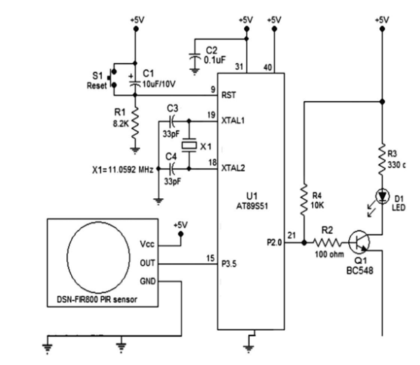
Figure 13. Interfacing of PIR sensor.
The output voltage will be 3.3V when the motion is detected and 0V when there is no motion. The sensing angle cone is 110° and the sensing range is 7 meters. The default delay time is 5 seconds. There are two preset resistor on the sensor module. One is used for adjusting the delay time and the other is used for adjusting the sensitivity.
Circuit Operation:
The circuit will read the status of the output of the PIR sensor and switch ON the LED when there is a motion detected and switch OFF the LED when there is no motion detected.
Output pin of the PIR sensor is connected to Port 3.5 pin of the 8051. Resistor R1, capacitor C1 and push button switch S1 forms the reset circuit. Capacitors C3,C4 and crystal X1 are associated with the oscillator circuit.
C2 is just a decoupling capacitor. LED is connected through Port 2.0 of the microcontroller. Transistor Q1 is used for switching the LED. R2 limits the base current of the transistor and R3 limits the current through the LED.
Program:
PIR EQU P3.5
LED EQU P2.0
ORG 00H
CLR P2.0
SETB P3.5
HERE:JNB PIR, HERE
SETB LED
HERE1:JB PIR,HERE1
CLR LED
SJMP HERE
END
Key takeaway
PIR sensors are widely used in motion detecting devices. It measures the amount of infrared energy radiated by objects in front of it.
They do not emit any kind of radiation but sense the infrared waves emitted or reflected by objects.
The heart of a PIR sensor is a solid- state sensor or an array of such sensors constructed from pyro-electric materials.
In these systems the microcontroller generates output in digital form, The controlling system requires analog signal because they don't accept digital data. Hence, there is a need to use DAC which converts digital data into its equivalent analog voltage.
- In the figure shown, we use 8-bit DAC 0808. This IC converts digital data into its equivalent analog current. The I to V converter converts the current into its equivalent voltage.
According to theory of DAC Equivalent analog output is given as:
 :
:
1. IF data =00H [00000000] and
Vref = 10V

Therefore, V0= 0 Volts.
2. If data is 80H [10000000],
And Vref = 10V

Therefore, V0= 5 Volts.
Different Analog output voltages for different Digital signal is given as:
DATA | OUTPUT VOLTAGE |
00H | 0V |
80H | 5V |
FFH | 10V |
Interfacing Diagram
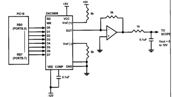
Figure 14. Interfacing PIC with DAC 0808
Generation of Sine wave
In order to generate sine wave we need table whose values represent the magnitude of the sine of angles between 0 and 360 degrees. The values for the sine function vary from -1.0 to +1.0 for 0 to 360 degree angles. To generate full scale output of the DAC is acheieved when all the data inputs of the DAC are HIGH. Therefore, to achieve the full scale 10V,
Vout =5V + (5 x sinΘ)
Angle θ(degrees) | Sin θ |   | Values Sent to DAC (decimal) |
0 | 0 | 5 | 128 |
30 | 0.5 | 75 | 192 |
60 | 0.866 | 9.33 | 238 |
90 | 1.0 | 10 | 255 |
120 | 0.866 | 9.33 | 238 |
150 | 0.5 | 7.5 | 192 |
180 | 0 | 5 | 128 |
210 | -0.5 | 2.5 | 64 |
240 | -0.866 | 0.669 | 17 |
280 | -1.0 | 0 | 0 |
300 | -0.866 | 0.669 | 17 |
330 | -0.5 | 2.5 | 64 |
360 | 0 | 5 | 128 |
Angle V/S voltage magnitude for Sine Wave is shown in above table. The below program sends the values to the DAC continuously to produce a sine wave.
OVER MOVLW upper(TABLE)
MOVWF TBLPTRU
MOVLW high(TABLE)
MOVWF TBLLPTRH
MOVLW low(TABLE)
MOVWF TBLPTRL
AGAIN TBLRD
MOVF TABLAT, W
XORLW 0X0
BZ OVER
MOVWF PORTB
INCF TBLPTRL, F
BRA AGAIN
ORG 0X250
TABLE: DB D’128’, D’192’, D’238’, D’255’, D’238’, D’192’
DB D’128’, D’64’, D’17’, D’1’, D’17’, D’64’, D’0’
END
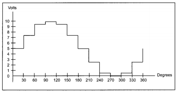
Fig 15 Angle V/S Magnitude for Sine Wave
Program in C
#include<p18F458.h>
Rom const unsigned char WAVEVALUE [12] = {128, 192, 238, 255, 238, 192, 128, 64, 17, 0, 17, 64}
Void main ()
{
Unsigned char x;
TRISB=0;
While(1)
{
For (x=0;x<12;x++)
PORTB= WAVEVALUE [x];
}
}
Key takeaway
In these systems the microcontroller generates output in digital form, The controlling system requires analog signal because they don't accept digital data. Hence, there is a need to use DAC which converts digital data into its equivalent analog voltage.
Design of PIC test board for verifying the LED connected to port B, with switches and Buzzer to port D, with relay interface for Port A.
The steps involved are:
- Design of Power Supply
- Design of clock circuit
- Design of Reset Circuit.
- Configuration of port
- Interfacing Diagram
- Program.
- Design of Power Supply
PIC 18F4550 works on the frequency of oscillator ranging from 0 to 20 MHz and requires power supply of ± 5 or ±12 V. A simple circuit design for +5 V is shown in Fig.

Figure 16. Design of +5V Power Supply
- Design of clock circuit
The Quartz crystal is connected to OSC1 and OSC2 pin in order to synchronize the operation of all components connected with internal and external means. The values for C1 and C2 are selected according to the crystal frequency for stabilizing the oscillator pulses. In general, with quartz crystal 22-33 µF is preferred.
- Design of Reset Circuit
The RC high pass filter with C=0.1µF along with 20 kΩ register is connected to MCLR pin. When high pulse appear on it, resets the contents of inter registers and SFRS to initial value.
- Configuration of port
PIC has 33 I/O lines which can be configured as input and output using TRISX register as
- If TRISX = 0 —Ports (A-E) are configured as output ports
- If TRISX = 1 —Ports (A-E) are configured as input ports.
- Interfacing
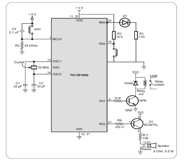
Figure 17. Minimum Connection PIC test board
Program
#include<P18F4550.h>
void delay(void);
void main()
{
unsigned char i, key;
TRISDbits.TRISD0 = 1;//set RD0 as input
TRISBbits.TRISB0 = 0;//set LED pin RB0 as output
TRISDbits.TRISD2 = 0;//set buzzer pin RD2 as output
TRISAbits.TRISA4 = 0;//set relay pin RA4 as output
while(1)
{
LATDbits.LD0 = 1; // RD0 pin as continuosly High
if(PORTDbits.RD0 == 0) // if switch is pressed
{
PORTBbits.RB0 = 1;//set led pin RB0 as High
delay();
PORTDbits.RD2 = 1;//set buzzer pin RD2 as High, Buzzer ON
delay();
PORTAbits.RA4 = 1;//set relay pin RA4 as High, Relay ON
delay();
}
else(PORTDbits.RD0 == 1) // if switch is pressed
{
PORTBbits.RB0 = 0;//set led pin RB0 as low, led off
delay();
PORTDbits.RD2 = 0;//set buzzer pin RD2 as low, Buzzer off
delay();
PORTAbits.RA4 = 0;//set relay pin RA4 as low, Relay Off
delay();
}
}
void delay()
{
unsigned int j,k;
for(j=0;j<=10;j++)
for(k=0;k<=3000;k++);
}
Key takeaway
Design of PIC test board for verifying the LED connected to port B, with switches and Buzzer to port D, with relay interface for Port A.
The steps involved are:
- Design of Power Supply
- Design of clock circuit
- Design of Reset Circuit.
- Configuration of port
- Interfacing Diagram
- Program.
A programming tool or software development tool is a computer program that software developers use to create, debug, maintain, or otherwise support other programs and applications. The term usually refers to relatively simple programs, that can be combined together to accomplish a task, much as one might use multiple hand tools to fix a physical object. The ability to use a variety of tools productively is one hallmark of a skilled software engineer. List of Tools
- Binary compatibility analysis tools
- Bug databases: Comparison of issue tracking systems - Including bug tracking systems
- Build tools: Build automation, List of build automation software
- Call graph
- Code coverage: Code coverage#Software code coverage tools.
- Code review: List of tools for code review
- Code sharing sites: Freshmeat, Krugle, Sourceforge, GitHub. See also Code search engines.
- Compilation and linking tools: GNU toolchain, gcc, Microsoft Visual Studio, CodeWarrior, Xcode, ICC
- Debuggers: Debugger#List of debuggers. See also Debugging.
- Disassemblers: Generally reverse-engineering tools.
- Documentation generators: Comparison of documentation generators, help2man, Plain Old Documentation, asciidoc
- Formal methods: Mathematical techniques for specification, development and verification
- GUI interface generators
- Library interface generators: SWIG
- Integration Tools
- Memory debuggers are frequently used in programming languages (such as C and C++) that allow manual memory management and thus the possibility of memory leaks and other problems. They are also useful to optimize efficiency of memory usage. Examples: dmalloc, Electric Fence, Insure++, Valgrind
- Parser generators: Parsing#Parser development software
- Performance analysis or profiling: List of performance analysis tool
- Revision control: List of revision control software, Comparison of revision control software
- Scripting languages: PHP, Awk, Perl, Python, REXX, Ruby, Shell, Tcl
- Search: grep, find
- Source code Clones/Duplications Finding: Duplicate code#Tools
- Source code editor
- Text editors: List of text editors, Comparison of text editors
- Source code formatting: indent
- Source code generation tools: Automatic programming #Implementations
- Static code analysis: lint, List of tools for static code analysis
- Unit testing: List of unit testing frameworks IDE Integrated development environments combine the features of many tools into one package. They for example make it easier to do specific tasks, such as searching for content only in files in a particular project.
- IDEs may for example be used for development of enterprise-level applications. Different aspects of IDEs for specific programming languages can be found in this comparison of integrated development environments.
Key takeaway
A programming tool or software development tool is a computer program that software developers use to create, debug, maintain, or otherwise support other programs and applications. The term usually refers to relatively simple programs, that can be combined together to accomplish a task, much as one might use multiple hand tools to fix a physical object. The ability to use a variety of tools productively is one hallmark of a skilled software engineer
Design a Home protection system to for indicating various parameters like temperature, door open /closed, internal apparatus on, which will give alert by indicator, display and sounding alarm if exceed the set point. Also make provision to store few current records in the serial memory for analysis.
- Design of Power Supply

Figure 18. Design of Power Supply
The microcontroller selected is PIC 18F4550 which works on the frequency of oscillator ranging from 0 to 20 MHz and requires power supply of ± 5 or ±12 V. A simple circuit design for +5 V is shown in Figure.
- Design of clock circuit
The Quartz crystal is connected to OSC1 and OSC2 pin in order to synchronize the operation of all components connected with internal and external means. The values for C1 and C2 are selected according to the crystal frequency for stabilizing the oscillator pulses. In general, with quartz crystal 22-33 µF is preferred.
- Design of Reset
The RC high pass filter with C=0.1µF along with 20 kΩ register is connected to MCLR pin. When high pulse appear on it, resets the contents of inter registers and SFRS to initial value.
PIC has 33 I/O lines which can be configured as input and out using TRISX register.
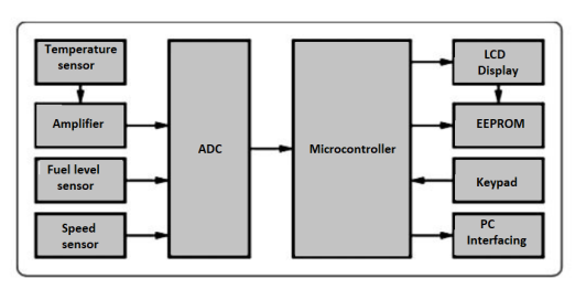
Figure 19. Block Diagram
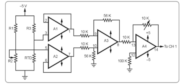
Figure 20. Signal Conditioning using Op-amp
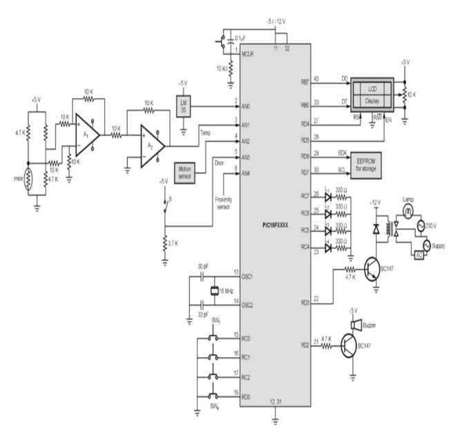
Figure 21. Interfacing Diagram for Home Protection system
CASE STUDIES OF PIC CONTROLLER
Multiplexed displays are electronic display devices where the entire display is not driven at one time. Instead, sub-units of the display (typically, rows or columns for a dot matrix display or individual characters for a character oriented display, occasionally individual display elements) are multiplexed, that is, driven one at a time, but the electronics and the persistence of vision combine to make the viewer believe the entire display is continuously active.
A multiplexed display has several advantages compared to a non-multiplexed display:
- Fewer wires (often, far fewer wires) are needed
- Simpler driving electronics can be used
- Both lead to reduced cost
- Reduced power consumption Multiplexed displays can be divided into two broad categories: 1. Character-oriented displays 2. Pixel-oriented displays
Character-oriented displays
Most character-oriented displays (such as seven-segment displays, fourteen-segment displays, and sixteen-segment displays) display an entire character at one time. The various segments of each character are connected in a two-dimensional diode matrix and will only illuminate if both the "row" and "column" lines of the matrix are at the correct electrical potential. The lightemitting element normally takes the form of a light-emitting diode (LED) so electricity will only flow in one direction, keeping the individual "row" and "column" lines of the matrix electrically isolated from each other. For liquid crystal displays, the intersection of the row and column is not conductive at all.
In the example of the VCR display shown above, the illuminated elements are the plates of many individual triode vacuum tubes sharing the same vacuum enclosure. The grids of the triodes are arranged so that only one digit is illuminated at a time. All of the similar plates in all of the digits (for example, all of the lower-left plates in all of the digits) are connected in parallel. One by one, the microprocessor driving the display enables a digit by placing a positive voltage on that digit's grid and then placing a positive voltage on the appropriate plates. Electrons flow through that digit's grid and strike those plates that are at a positive potential. If the display had been built with every segment being individually connected, the display would have required 49 wires just for the digits, with more wires being needed for all of the other indicators that can be illuminated. By multiplexing the display, only seven "digit selector" lines and seven "segment selector" lines are needed. The extra indicators (in our example, "VCR", "Hi-Fi", "STEREO", "SAP", etc.) are arranged as if they were segments of an additional digit or two or extra segments of existing digits and are scanned using the same multiplexed strategy as the real digits. Most character-oriented displays drive all the appropriate segments of an entire digit simultaneously.
A few character-oriented displays drive only one segment at a time. The display on the Hewlett-Packard HP-35 was an example of this. The calculator took advantage of an effect of pulsed LED operation where very brief pulses of light are perceived as brighter than a longer pulse of light with the same time-integral of intensity. A keyboard matrix circuit has a very similar arrangement as a multiplexed display, and has many of the same advantages. In order to reduce the number of wires even further, some people "share" wires between a multiplexed display and a keyboard matrix, reducing the number of wires even further.
Pixel-oriented displays
By comparison, in dot matrix displays, individual pixels are located at the intersections of the matrix's "row" and "column" lines and each pixel can be individually controlled. Here, the savings in wiring becomes far more dramatic. For a typical 1024x768 (XGA) computer screen, 2,359,296 wires would be needed for non-multiplexed control. That many wires would be completely impractical. But by arranging the pixels into a multiplexed matrix, only 1792 wires are needed; a completely practical situation. Pixel-oriented displays may drive a single pixel at a time or an entire row or column of pixels simultaneously. Active-matrix liquid crystal displays provide a storage element at each pixel so that the pixel continues to display the correct state even when not being actively driven.
References:
1. Kenneth J. Ayala, ‘The 8051 Microcontroller Architecture, Programming and Applications’, Cengage Learning, 3rd Edition
2. Ajay Deshmukh, “Microcontrollers Theory and Applications”, TATA McGraw Hill, 4th Edition
3. Peatman, John B, “Design with PIC Microcontroller”, Pearson Education PTE, 1st Edition
4. Data Sheet of PIC 18Fxxxx series