Unit 2
Combinational Logic Design
- Half Adder
It is a combinational circuit that has two inputs and two outputs.
It is designed to add two single bit binary numbers A and B.
It has two outputs carry and sum.
Block diagram
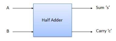
Fig. : A half adder (ref. 2)
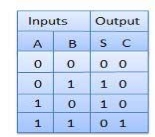
Truth Table
Circuit Diagram
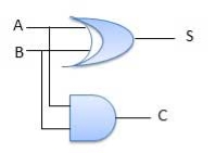
Fig.: A half adder (ref. 2)
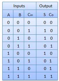
B. Full Adder
It is developed to overcome the drawback of the Half Adder circuit.
It can add two one-bit numbers A and B and a carry C.
It is a three-input and two output combinational circuit.
Block diagram
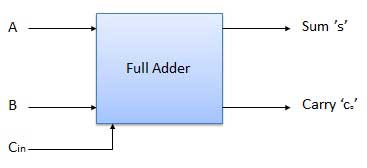
Fig.: Full adder (ref. 2)
Truth Table
Circuit Diagram
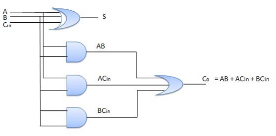
Fig.: Full adder (ref. 2)
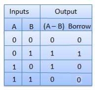
C. Half Subtractors
It is a combination circuit with two inputs and two outputs.
The difference between the two binary bits is obtained at the output and an output (Borrow) indicates if a 1 has been borrowed.
Here A is called Minuend bit and B is called a Subtrahend bit.
Truth Table
Circuit Diagram
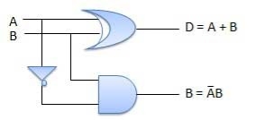
Fig.: Half subtractor (ref. 2)
D. Full Subtractors
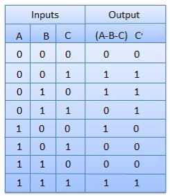
It is a combinational circuit which has three inputs A, B, C, and two output D and C'.
A is the 'minuend', B is 'subtrahend', C is the 'borrow' which is produced by the previous stage, difference output D and C' is the borrow output.
Truth Table
Circuit Diagram
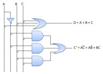
Fig.: Full subtractor (ref. 2)
E. BCD Adder
BCD stands for binary coded decimal.
Suppose, we have two 4-bit numbers A and B. The value of A and B can vary from 0(0000 in binary) to 9(1001 in binary).
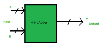
Fig. : BCD adder (ref. 2)
The output varies from 0 to 18 if the carry from the previous sum is not considered.
But if we consider the carry, then the maximum value of output will be 19 (i.e. 9+9+1 = 19).
When we simply add A and B, then we get the binary sum, and to get the output in BCD form, we use BCD Adder.
Example 1:
Input :
A = 0111 B = 1000
Output :
Y = 1 0101
Explanation: We are adding A(=7) and B(=8).
The value of the binary sum will be 1111(=15).
But, the BCD sum will be 1 0101,
Where 1 is 0001 in binary and 5 is 0101 in binary.
Example 2:
Input :
A = 0101 B = 1001
Output :
Y = 1 0100
Explanation: We are adding A(=5) and B(=9).
The value of the binary sum will be 1110(=14).
But, the BCD sum will be 1 0100,
Where 1 is 0001 in binary and 4 is 0100 in binary.
Now, let's move to the table and find out the logic when we are going to add “0110”.
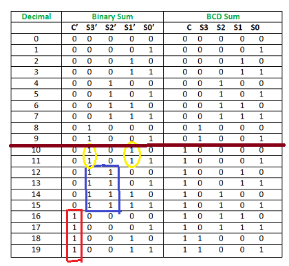
Fig. : Table explaining BCD addition (ref. 2)
We are adding “0110” (=6) only to the second half of the table because of the following conditions:
- If C’ = 1 (Satisfies 16-19)
- If S3′.S2′ = 1 (Satisfies 12-15)
- If S3′.S1′ = 1 (Satisfies 10 and 11)
So, our logic is
C' + S3'.S2' + S3'.S1' = 1
Implementation :
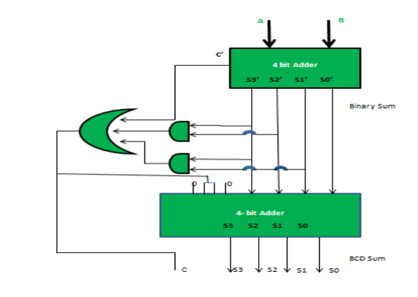
Fig: BCD adder (ref. 2)
- It is a special type of combinational circuit.
- It has n-data inputs, one output, and m inputs select lines with 2m = n.
- It selects one of the n data inputs and routes it to the output.
- The selection of one of the inputs is done by the select lines.
- Depending on the code applied at the inputs, one of the n data sources is selected and transmitted to the single output Y.
- E is the enable input which is useful for cascading purposes.
- It is an active low terminal hence performs the required operation when it is low.
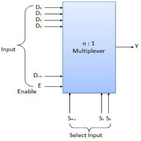
Fig. : Block diagram of the multiplexer (ref. 2)
Multiplexers come in multiple variations
- 2: 1 multiplexer
- 4: 1 multiplexer
- 16: 1 multiplexer
- 32: 1 multiplexer
Block Diagram of 2:1 MUX
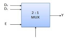
Truth Table of 2:1 MUX
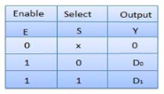
Where x is don’t care.
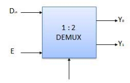
Demultiplexers
- It performs the inverse operation of a multiplexer as it receives one input and distributes it across its outputs.
- It has only one input and n outputs with m select input.
- At a time only one output line is selected by the select lines and that input is transmitted through the output line.
- It is equivalent to a single-pole multiple-way switch.
Various Demultiplexers are used as:
- 1: 2 demultiplexer
- 1: 4 demultiplexer
- 1: 16 demultiplexer
- 1: 32 demultiplexer
Block diagram
Truth Table
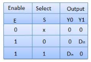
Where x is don’t care.
- It works as an inverse of an encoder.
- It is a combinational circuit which converts n input lines into 2n output lines.
- Taking an example of 3-to-8 line decoder.
Truth Table –
X | Y | Z | D0 | D1 | D2 | D3 | D4 | D5 | D6 | D7 |
0 | 0 | 0 | 1 | 0 | 0 | 0 | 0 | 0 | 0 | 0 |
0 | 0 | 1 | 0 | 1 | 0 | 0 | 0 | 0 | 0 | 0 |
0 | 1 | 0 | 0 | 0 | 1 | 0 | 0 | 0 | 0 | 0 |
0 | 1 | 1 | 0 | 0 | 0 | 1 | 0 | 0 | 0 | 0 |
1 | 0 | 0 | 0 | 0 | 0 | 0 | 1 | 0 | 0 | 0 |
1 | 0 | 1 | 0 | 0 | 0 | 0 | 0 | 1 | 0 | 0 |
1 | 1 | 0 | 0 | 0 | 0 | 0 | 0 | 0 | 1 | 0 |
1 | 1 | 1 | 0 | 0 | 0 | 0 | 0 | 0 | 0 | 1 |
Implementation
D0 is high when X = 0, Y = 0 and Z = 0. Hence,
D0 = X’ Y’ Z’
Similarly,
D1 = X’ Y’ Z
D2 = X’ Y Z’
D3 = X’ Y Z
D4 = X Y’ Z’
D5 = X Y’ Z
D6 = X Y Z’
D7 = X Y Z
Hence,
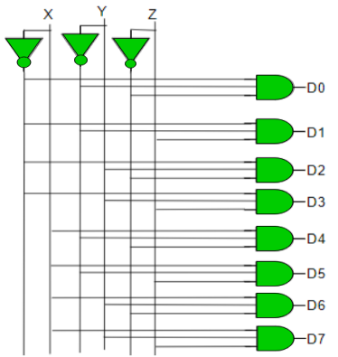
Fig: Decoder
- It is an encoder whose inputs are given priorities.
The BCD adder IC 7483 is shown below. It is a 16-pin chip. The pin configuration is explained below. When two IC connected in series adds the eight bit number.
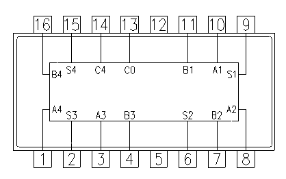
Fig: IC 7483
Pin1: A4 input
Pin2: S3 (sum output bit)
Pin3: A3 input
Pin4: B3 input
Pin5: Supply (Vcc)
Pin6: S2 (Sum output bit)
Pin7: B2 input
Pin8: A2 input
Pin9: S1 sum output bit
Pin10: A1 input
Pin11: B1 input
Pin12: Ground
Pin13: C0 input
Pin14: C4 input
Pin15: S4 output
Pin16: B4 input
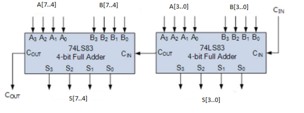
The above figure shows a 4-bit full adder using IC 7483. It is a 16 pin IC. The IC consists of four interconnected full adders with a look ahead carry generator. The adder adds two number A and B each of four bits. The adder adds these numbers and produce a carry bit Cout. The first adder adds the LSB of both numbers (A0-A3 and B0 -B3). The sum produced after addition is S0-S3 and a carry bit Cout. The carry generated from first adder is input to the second CIN. The second adder adds the MSB of both numbers giving a sum (S4-S7) along with carry.
The 4-bit BCD adder is shown below using IC 7483. As we already know that a BCD number cannot be greater than 9. So, when the digits are added the sum should be less than 9 and with carry 0. But if the case is otherwise, then a combinational circuit is needed additionally in the circuit. This combinational circuit checks the sum if less than 9 or not, if not than correction is required. The output of the combinational circuit will be high if Cout from adder-1 is not 0.
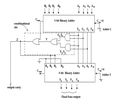
The output Y is ORed with Cout. The output Z of the combinational circuit will be high if Cout is not zero. Hence, making the bits B1 and B2 of adder-2 high. If Cout =1 then, B3B2B1B0 of adder-2 will be 0110. The sum from adder-1 is connected to adder-2 and the carry generated here is discarded.
The truth table of BCD number is shown below.
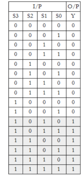
The k-map for the combinational circuit along with truth table is shown below.
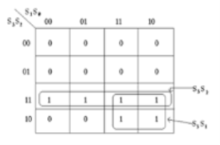
The output expression will be Y= S3S2+S3S1
Let’s consider one example addition of two BCD numbers A=0111 and B= 1001.
0111
 +1001
+1001
10000
Cout = 1
So, output Z of combinational circuit will be high i.e Z=1. The sum output of adder-1(S3-S0) =0000 is input to LSB of adder-2. As Z=1, B3B2B1B0 of adder-2 will be 0110. So, the final output from adder-2 (S3-S0) will be 0110 and carry as 1(0001).
Therefore, (0111) BCD+(1001) BCD = (00010110) BCD
Half Subtractor:
The change we need to make in the above arrangement to make it work as a subtractor is that the minuend is connected the way it was. We just negate the bits of subtrahend before connecting, and then add the numbers which gives the difference as output.
If A=1000 B=0110
We need to find A-B
So, we first find 2’s compliment of B = 1010
Then adding both 1000+1010= 0010 and the carry is discarded.
IC 74153 is a multiplexer. Here we will implement half adder, full adder, half subtractor and full subtractor.
1) The Pin 16 is connected to + Vcc.
2) Pin 8 is connected to ground.
3) The inputs are applied either to ‘A’ input or ‘B’ input.
4) If MUX ‘A’ has to be initialized, Ea is made low and if MUX ‘B’ has to be initialized, Eb is made low.
5) Based on the selection lines one of the inputs will be selected at the output and thus the truth table is verified.
6) In case of half adder using MUX, sum and carry is obtained by applying a constant input at I0a, I1a, I 2a, I 3a and I 0b, I 1b, I 2b and I3b and the corresponding values of select lines are changed as per table and the output is taken at Z0a as sum and Z0b as carry.
7) In this case, the channels A and B are kept at constant inputs according to the table and the inputs A and B are varied. Making Ea and Eb zero and the output is taken at Za, and Zb.
8) In full adder using MUX, the input is applied at Cn-1, An and Bn. According to the table corresponding outputs are taken at Cn and Dn.
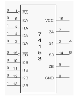
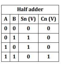
Fig: Half Adder using IC 74153
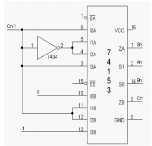
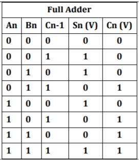
Fig: Full Adder using IC 74153
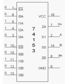
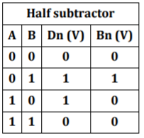
Fig: half Subtractor using IC 74153
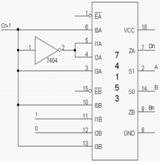
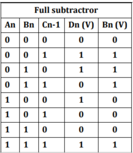
Fig: Full Subtractor using IC 74153