Unit - 2
Data Acquisition and Signal Communication
Types of Communication system
1)Synchronous transmission
In synchronous transmission, data moves in a completely paired approach, in the form of chunks or frames. Synchronisation between the source and target is required so that the source knows where the new byte begins, since there are no spaces included between the data. Synchronous transmission is effective, dependable, and often utilised for transmitting a large amount of data. It offers real-time communication between linked devices. An example of synchronous transmission would be the transfer of a large text file. Before the file is transmitted, it is first dissected into blocks of sentences. The blocks are then transferred over the communication link to the target location.
Characteristics of Synchronous Transmission
- There are no spaces in between characters being sent.
- Timing is provided by modems or other devices at the end of the transmission.
- Special ’syn’ characters go before the data being sent.
- The syn characters are included between chunks of data for timing functions.
Examples of Synchronous Transmission
- Chatrooms
- Video conferencing
- Telephonic conversations
- Face-to-face interactions
2)Asynchronous Transmission
In asynchronous transmission, data moves in a half-paired approach, 1 byte or 1 character at a time. It sends the data in a constant current of bytes. The size of a character transmitted is 8 bits, with a parity bit added both at the beginning and at the end, making it a total of 10 bits. It doesn’t need a clock for integration—rather, it utilises the parity bits to tell the receiver how to translate the data. It is straightforward, quick, cost-effective, and doesn’t need 2-way communication to function.
Characteristics of Asynchronous Transmission
- Each character is headed by a beginning bit and concluded with one or more end bits.
- There may be gaps or spaces in between characters.
Examples of Asynchronous Transmission
- Emails
- Forums
- Letters
- Radios
- Televisions
3)Serial Transmission
In serial communication, there is a single channel between the sender and receiver. In this method, the bits line up at the receiver, and each bit travels through the channel one at a time.
4) Parallel Transmission
In parallel communication, multiple bits sent through the channels or buses simultaneously. Assume that there are three bits to transmit. Then, they will go through three separate lines from sender to receiver.
Key takeaway
Differences between serial and parallel Transmission
Serial vs Parallel Communication | |
The process of sending data one bit at a time, sequentially over a communication channel or a computer bus. | The process of sending multiple bits as a whole on a link with several parallel channels or computer buses. |
Required Number of Lines | |
Uses a single line to send data | Uses several lines to transmit data |
Speed | |
Slow for short distances and low frequencies but higher in long distances and high frequencies | Fast for short distance and low frequencies but slower in long distances and high frequencies |
Error and Noise | |
Error and Noise are minimum | Error and noise are high |
Nature | |
Simple and straightforward | Unreliable and complicated |
Cost | |
Cost is comparatively lower | Cost is higher in comparison |

Fig 1 DAQ system
Data acquisition (DAQ) is the process of measuring an electrical or physical phenomenon such as voltage, current, temperature, pressure, or sound with a computer. A DAQ system consists of sensors, DAQ measurement hardware, and a computer with programmable software. Compared to traditional measurement systems, PC-based DAQ systems exploit the processing power, productivity, display, and connectivity capabilities of industry-standard computers providing a more powerful, flexible, and cost-effective measurement solution.
We can sort digital data acquisition systems types according to several important criteria:
- Data Acquisition Systems by Form Factor: From small computer-connected modules to stand-alone systems.
- Data acquisition systems by Distributability: Modularity and interoperability of acquisition nodes.
- Data acquisition systems by Speed: How fast they can sample data.
- Data acquisition systems by IP Environmental Protection: The ability to withstand shock, vibration, dust, water, and temperature extremes.
- Data acquisition systems by Control Capabilities: The ability to integrate with real-time control systems.
Data acquisition is a term that encompasses a wide range of measurement applications, all of which require some form of characterization, monitoring, or control.
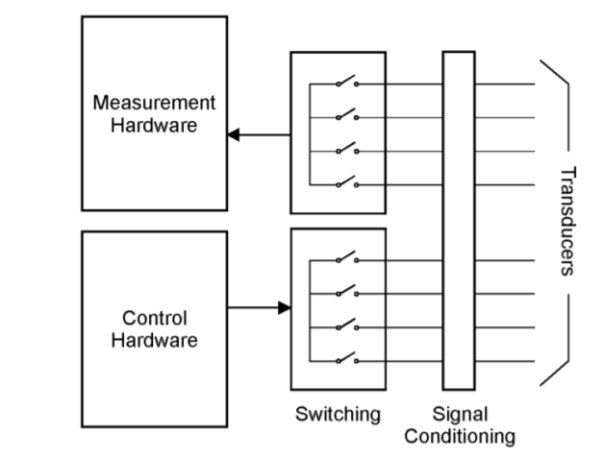
Fig 3 Data Acquisition System
A/D Converter: The A/D converter, a key element in any data acquisition system, is used to convert dc voltages acquired from the transducers into digital data. The measured voltages may correspond to a specific temperature, pressure, flow, or speed. While there are several types of A/D conversion techniques, they can generally be divided into two types: integrating and nonintegrating. The integrating techniques measure the average input value over a defined time interval, thereby rejecting many noise sources. The non-integrating techniques sample the instantaneous value of the input (plus noise) during a very short time interval.
Digital Input: Some data acquisition systems contain a digital input card that senses a digital bit pattern to determine whether an external device is on or off. Digital input cards typically contain 8, 16, or 32 channels that can be used to monitor a number of external devices. For example, a digital input card can be connected to an operator panel to determine the position of various switches on the panel.
Control Switching: For control applications, a switching card can be used to supply power to external fans, pumps, or valves by completing an electrical circuit. The switch card (often referred to as an actuator) operates much like a light switch to provide power to the external device. A switch card is typically used instead of a digital output card in those applications that require switching of high voltage and power. There are three common types of switches used in control applications.
Switching Electromechanical switches, such as reed and armature relays, are common in low-speed applications. A key benefit is their ability to switch high voltage and current levels, but they are limited to switching rates of several hundred channels per second. Also, because they are mechanical devices, they will eventually wear out. Electronic switches, such as field-effect transistors (FETs) and solid-state relays, are typically used in highspeed applications. In addition to providing fast switching, they contain no moving parts and therefore do not wear out. The disadvantage of electronic switches is that they typically cannot handle high voltage or current, and must be carefully protected from input spikes and transients.
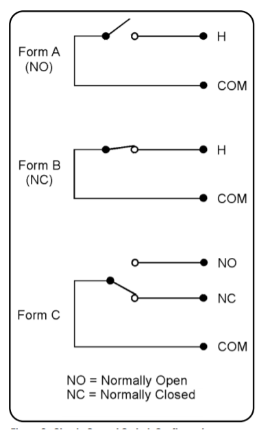
Fig 4 Switching System
Signal Conditioning Signal conditioning is used to amplify, attenuate, shape, or isolate signals from transducers before they are sent to the measurement hardware. Signal conditioning converts the signal to a form that is better measured by the system, or in some cases, makes it possible to measure the signal at all. Examples of signal conditioning include:
- Amplification of small signals
- Attenuation of large signals
- Thermocouple compensation for temperature measurements
- Current sourcing for 2-wire and 4-wire resistance measurements
- Filtering to remove system noise
- Shunt resistors for current measurements
In some data acquisition systems, the signal conditioning components are incorporated internally within the system. These systems can measure dc voltage, ac voltage, resistance, frequency, current, and temperature on any input channel without the need for external signal-conditioning components.
Sensors: Sensors and transducers are devices that transform physical parameters (such as temperature, pressure, flow, and strain) into electrical parameters (such as voltage, current, and resistance). The electrical parameter is measured by measurement hardware and the result is converted to engineering units. For example, when measuring a thermocouple, the measurement hardware actually reads a dc voltage, which it then converts to a corresponding temperature using a mathematical algorithm. The following table shows several types of transducers with their corresponding output.
Key takeaway
The A/D converter, a key element in any data acquisition system, is used to convert dc voltages acquired from the transducers into digital data. The measured voltages may correspond to a specific temperature, pressure, flow, or speed. While there are several types of A/D conversion techniques, they can generally be divided into two types: integrating and nonintegrating.
All industrial processing systems, factories, machinery, test facilities, and vehicles consist of hardware components and computer software whose behavior follow the laws of physics as we understand them. These systems contain thousands of mechanical and electrical phenomena that are continuously changing; they are not steady state. The measurable quantities that represent the characteristics of all systems are called variables. The proper functioning of a particular system depends on certain events in time and the parameters of these variables. Often, we are interested in the location, magnitude, and speed of the variables, and we use instruments to measure them.
We assign the variables units of measure such as volts, pounds, and miles per hour, to name a few. Most variables must be measured with a device that converts the phenomena into a form that a human can perceive such as a visual display, a transducer for sound, or vibrations to stimulate physical sensations. The conversion devices are called transducers or sensors, and they translate the physical phenomena to electrical signals (or vice versa) to be measured with electronic instruments. These instruments have traditionally been ammeters, voltmeters, and various other gages, and the variables can be observed in real time. But an increasing need to record and preserve these phenomena and analyse them at a later time forced engineers to develop data recorders and data acquisition systems.
Variables may be classified in many ways, but generally, most experts prefer two classifications: by characteristic and by type of measurement signal. Variables classified by characteristic include thermal, radiation, force, rate, quantity, time, geometric, physical properties, chemical composition, and electrical. Those classified by measurement signal include motion, force, electrical, and time-modulated. Measurement signals for variables often are hard to differentiate from the measuring system. Four factors require close consideration for measurement signals and systems: the types of transducers available for converting variables to measurement signals, transmission characteristics, data acquisition system input matching, and transducers available to convert from one type of measurement signal to another measurement signal.
Key takeaway
All industrial processing systems, factories, machinery, test facilities, and vehicles consist of hardware components and computer software whose behavior follow the laws of physics as we understand them. These systems contain thousands of mechanical and electrical phenomena that are continuously changing; they are not steady state.
Frequently, data acquisition system inputs must measure low-level signals where relatively high voltages are common, such as in motor controllers, transformers, and motor windings. In these cases, isolation amplifiers can measure low-level signals among high common-mode voltages, break ground loops, and eliminate source ground connections without subjecting operators and equipment to the high voltage. They also provide a safe interface in a hospital between a patient and a monitor or between the source and other electronic instruments and equipment. Yet other applications include precision bridge isolation amplifiers, photodiode amplifiers, multiple-port thermocouple and summing amplifiers, and isolated 4 to 20 mA current-control loops.
Isolation Amplifiers
Isolation amplifiers are divided into input and output sections, galvanically isolated from each other. Several techniques provide the isolation; the most widely used include capacitive, inductive, and optical means. The isolation voltage rating is usually 1,200 to 1,500 Vac, at 60 Hz with a typical input signal range of ±10 V. They normally have a high isolation mode rejection (IMR) ratio of around 140 dB. Because the primary job of relatively low-cost amplifiers is to provide isolation, many come with unity gain. But more expensive units are available with adjustable or programmable gains.
Analog Isolation Modules
Analog isolation amplifiers use all three types of isolation between input and output sections: capacitive, optical, and magnetic. One type of capacitively coupled amplifier modulates the input signal and couples it across a capacitive barrier with a value determined by the duty cycle. The output section demodulates the signal, restores it to the original analog input equivalent, and filters the ripple component, which resulted from the demodulation process. After the input and output sections of the integrated circuit are fabricated, a laser trims both stages to precisely match their performance characteristics. Then they are mounted on either end of the package separated by the isolation capacitors. Although the schematic diagram of the isolation amplifier looks quite simple, it can contain up to 250 or more integrated transistors.
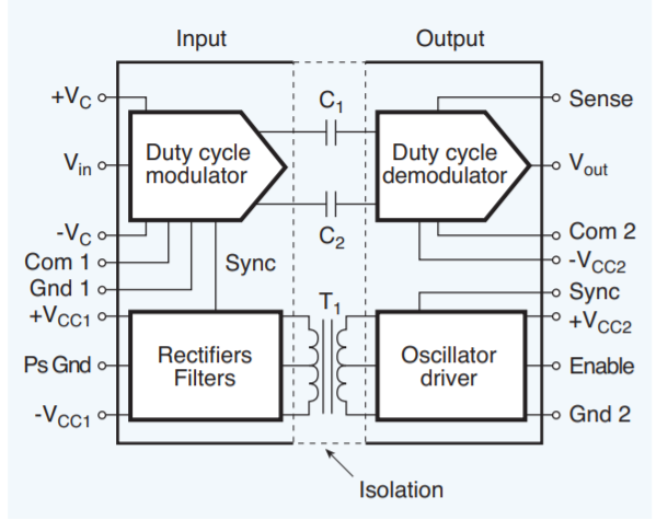
Fig 5 Isolation barrier
Digital Method of Isolation
In addition to directly measuring voltage, current, and resistance, which require some degree of isolation, certain sensors that measure other quantities are inherently isolated by virtue of their construction or principle of operation. The most widely used sensors measure position, velocity, pressure, temperature, acceleration, and proximity. They also use a number of different devices to measure these quantities, including potentiometers, LVDTs (linear variable differential transformers), optical devices, Hall-effect devices, magnetic devices, and semiconductors. Hall-effect devices, for example, measure magnetic fields, and are electrically insulated from the magnetic source that they are designed to measure. The insulation may be air or another material such as plastic or ceramic, and the arrangement essentially isolates them from ground loops and high voltages. Figures A and B illustrate two applications where Hall-effect devices measure speed. The first senses the alternating magnetic field directly from the revolving wheel. In the second application, a permanent magnet sitting behind the Hall effect device supplies the magnetic field. The gear teeth passing by the unit disturb the field, and the Hall device senses the resulting fluctuations. In addition, Figure 4.08. Shows a third example, where the Hall-effect device is used in a wattmeter circuit. Current transformers and potential transformers for measuring ac voltage and current are also inherently isolated between primary and secondary windings.
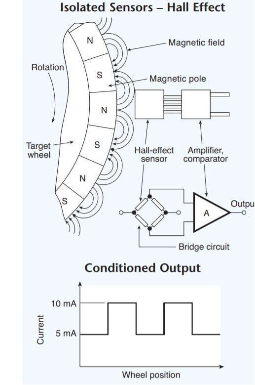
Fig.6 A. This Hall-Effect sensor is switched with a series of alternating magnets in a target wheel. Each pass between N and S magnets changes the sensor’s state.
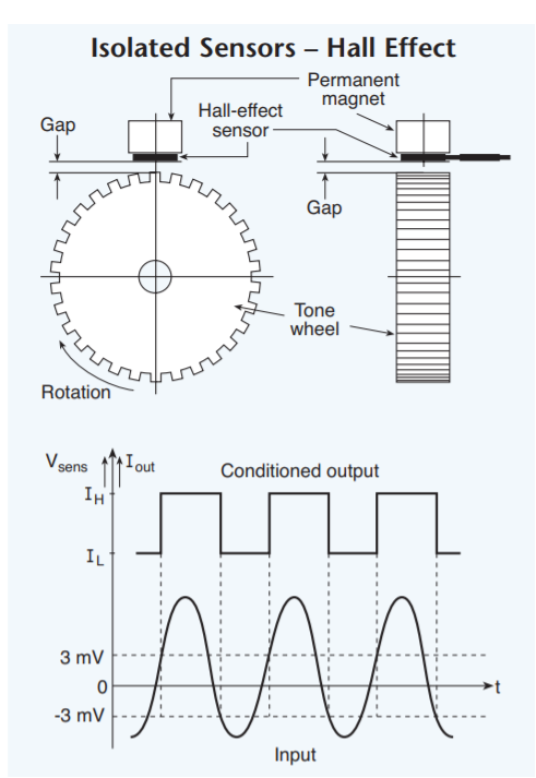
Fig. 6B. This Hall-Effect sensor configuration uses a bias magnet and a tone wheel that modulates the magnetic field intensity to produce an output signal.
Filtering
The term filtering is used to describe the process of removing a certain band of frequencies from a signal and permitting others to be transmitted. The range of frequencies passed by a filter is known as the pass band, the range not passed as the stop band and the boundary between stopping and passing as the cut-off frequency. Filters are classified according to the frequency ranges they transmit or reject. A low-pass filter has a pass band which allows all frequencies from zero up to some frequency to be transmitted. A high-pass filter has a pass band which allows all frequencies from some value up to infinity to be transmitted. A band-pass filter allows all the frequencies within a specified band to be transmitted. A band-stop filter stops all frequencies with a particular band from being transmitted. In all cases the cut-off frequency is defined as being that at which the output voltage is 70.7% of that in the pass band. The term attenuation is used for the ratio of input and output powers, this being written as the ratio of the logarithm of the ratio and so gives the attenuation in units of bels. Since this is a rather large unit, decibels (dB) are used and then attenuation in dB=10 log (input power/output power).
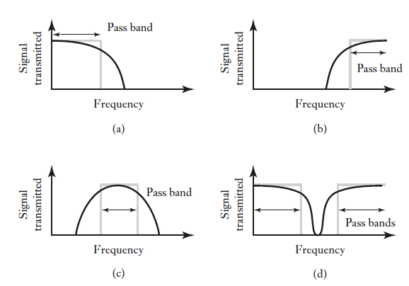
Fig 7 Characteristics of ideal filters: (a) low-pass, (b) high-pass, (c) band-pass, (d) band-stop.
Key takeaway
Isolation amplifiers are divided into input and output sections, galvanically isolated from each other. Several techniques provide the isolation; the most widely used include capacitive, inductive, and optical means. The isolation voltage rating is usually 1,200 to 1,500 Vac, at 60 Hz with a typical input signal range of ±10 V. They normally have a high isolation mode rejection (IMR) ratio of around 140 dB.
Inverting Amplifier
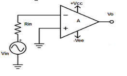
Fig.8: Inverting op-amp
- As seen in the above figure, input is applied to only one terminal i.e., inverting input terminal.
- The other input terminal is supplied 0V i.e., grounded.
- Hence,
V1 = 0V and V2 = Vin
- Therefore, output voltage Vout is given by,
Vout = A (- Vin)
Where, A is the voltage gain of op-amp.
- The negative sign implies that the output voltage is 1800 out of phase w.r.to the input voltage.
- Hence, the inverting amplifier amplifies the input signal by voltage gain A and inverts it at the output.
Non-Inverting Amplifier
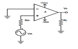
Fig.9: Non inverting amplifier
- As seen in the above figure, input is applied to only one terminal i.e., non-inverting input terminal.
- The other input terminal is supplied 0V i.e., grounded.
- Hence,
V1 = Vin and V2 = 0V
- Therefore, output voltage Vout is given by,
Vout =AVin
Where, A is the voltage gain of op-amp.
- Here, the output voltage is more than the input voltage by voltage gain A and are also in phase with each other.
Differential Amplifier configurations
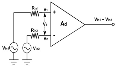
Fig.10: Differential Amplifier
- Vin1 and Vin2 are the two input signals applied at the positive and negative terminals of op-amp.
- Vout is the desired output voltage whose value is equal to the amplified difference between the input voltages.
- Op-amp can amplify both ac and dc voltages hence, the input supply voltages can both be ac or dc.
- Rin1 and Rin2 are source resistances and is negligible w.r.to input resistance Rin.
- Therefore, the voltage drops across them is also assumed to be zero.
- Hence the output voltage,
Vout= Ad (Vin1 - Vin2)
Where, Ad is known as open loop gain.
- Hence the output voltage is directly proportional to the product of voltage gain and difference between input voltages.
- The polarity of output voltage depends upon polarity of the difference between input voltages.
Programmable-Gain Amplifiers
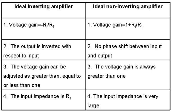
Programmable gain amplifiers are typically non-inverting operational amplifiers with a digitally controlled analog switch connected to several resistors in its feedback loop. An external computer or another logic or binary signal controls the addressable inputs of the analog switch so it selects a certain resistor for particular gain. The data acquisition system’s signal conditioners sense the input signal amplitude and automatically send the proper binary code to the programmable gain amplifier (PGA) to increase the gain for a low signal, or decrease the gain for a large signal. The input signal then can be measured and displayed without distortion.
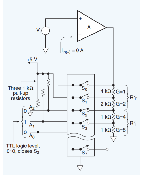
Fig 11 Programmable gain Amplifier
Instrumentation amplifier
The Instrumentation amplifiers consist of three op-amps. In this circuit, a non-inverting amplifier is connected to each input of the differential amplifier.
This instrumentation amplifier provides high input impedance for exact measurement of input data from transducers. The circuit diagram of an instrumentation amplifier is as shown in the figure below.
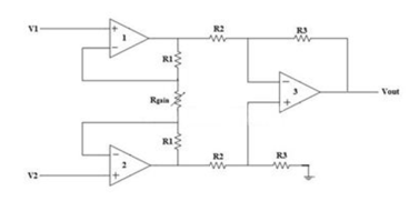
Fig 12 Instrumentation Amplifier
The op-amps 1 & 2 are non-inverting amplifiers and together form an input stage of the instrumentation amplifier. The op-amp 3 is a difference amplifier that forms the output stage of the instrumentation amplifier.
Working
The output stage of the instrumentation amplifier is a difference amplifier, whose output Vout is the amplified difference of the input signals applied to its input terminals.
If the outputs of op-amp 1 and op-amp 2 are Vo1 and Vo2 respectively, then the output of the difference amplifier is given by,
Vout = (R3/R2) (Vo1-Vo2)
The expressions for Vo1 and Vo2 can be found in terms of the input voltages and resistances.
Consider the input stage of the instrumentation amplifier as shown in the figure below.
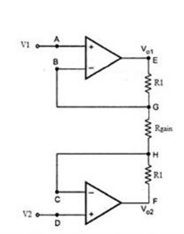
Fig 13 Input Stage of Instrumentation Amplifier
The potential at node A is the input voltage V1. Hence the potential at node B is also V1, from the virtual short concept. Thus, the potential at node G is also V1.
The potential at node D is the input voltage V2. Hence the potential at node C is also V2, from the virtual short. Thus, the potential at node H is also V2.
Ideally the current to the input stage op-amps is zero. Therefore, the current I through the resistors R1, Rgain and R1 remains the same.
Applying Ohm’s law between the nodes E and F,
I = (Vo1-Vo2)/(R1+Rgain+R1) ——————— 1
I = (Vo1-Vo2)/(2R1+Rgain)
Since no current is flowing to the input of the op-amps 1 & 2, the current I between the nodes G and H can be given as,
I = (VG-VH)/Rgain = (V1-V2)/Rgain ————————- 2
Equating equations 1 and 2,
(Vo1-Vo2)/(2R1+Rgain) = (V1-V2)/Rgain
(Vo1-Vo2) = (2R1+Rgain)(V1-V2)/Rgain —————— 3
The output of the difference amplifier is given as,
Vout = (R3/R2) (Vo1-Vo2)
Therefore, (Vo1 – Vo2) = (R2/R3)Vout
Substituting (Vo1 – Vo2) value in the equation 3, we get
(R2/R3)Vout = (2R1+Rgain)(V1-V2)/Rgain
i.e., Vout = (R3/R2) {(2R1+Rgain)/Rgain}(V1-V2)
The above equation gives the output voltage of an instrumentation amplifier. The overall gain of the amplifier is given by the term (R3/R2){(2R1+Rgain)/Rgain}.
Key takeaway
A signal has three properties like voltage or amplitude, frequency, phase. The signals are represented only in an analogy form where the digital form of technology is not available. Analog signals are continuous in time and difference in voltage levels for different periods of the signal. Here, the main drawback of this is, the amplitude keeps on changing along with the period of the signal. This can be overcome by the digital form of signal representation. Here conversion of an analogy form of the signal into digital form can be done using the sampling technique. The output of this technique represents the discrete version of its analog signal. Here in this article, you can find what is sampling theorem, definition, applications, and its types.
Sampling Theorem Definition
The sampling theorem can be defined as the conversion of an analog signal into a discrete form by taking the sampling frequency as twice the input analogy signal frequency. Input signal frequency denoted by Fm and sampling signal frequency denoted by Fs.
Sampling frequency
The output sample signal is represented by the samples. These samples are maintained with a gap, these gaps are termed as sample period or sampling interval (Ts). And the reciprocal of the sampling period is known as “sampling frequency” or “sampling rate”. The number of samples is represented in the sampled signal is indicated by the sampling rate.
Sampling frequency Fs=1/Ts
Sampling Theorem Statement
Sampling theorem states that “continues form of a time-variant signal can be represented in the discrete form of a signal with help of samples and the sampled (discrete) signal can be recovered to original form when the sampling signal frequency Fs having the greater frequency value than or equal to the input signal frequency Fm.
Fs ≥ 2Fm
If the sampling frequency (Fs) equals twice the input signal frequency (Fm), then such a condition is called the Nyquist Criteria for sampling. When sampling frequency equals twice the input signal frequency is known as “Nyquist rate”.
Fs=2Fm
Key takeaway
Sampling frequency Fs=1/Ts
Fs ≥ 2Fm
Aliasing effect
If the sampling frequency (Fs) is less than twice the input signal frequency, such criteria called an Aliasing effect.
Fs<2Fm
So, there are three conditions that are possible from the sampling frequency criteria. They are sampling, Nyquist and aliasing states.
Application of sampling theorem
There are few applications of sampling theorem are listed below. They are
- To maintain sound quality in music recordings.
- Sampling process applicable in the conversion of analog to discrete form.
- Speech recognition systems and pattern recognition systems.
- Modulation and demodulation systems
- In sensor data evaluation systems
- Radar and radio navigation system sampling is applicable.
- Digital watermarking and biometric identification systems, surveillance systems.
The Sample and Hold circuit is an electronic circuit which creates the samples of voltage given to it as input, and after that, it holds these samples for the definite time. The time during which sample and hold circuit generates the sample of the input signal is called sampling time. Similarly, the time duration of the circuit during which it holds the sampled value is called holding time.
Sampling time is generally between 1µs to 14 µs while the holding time can assume any value as required in the application. It will not be wrong to say that capacitor is the heart of sample and hold circuit. This is because the capacitor present in it charges to its peak value when the switch is opened, i.e., during sampling and holds the sampled voltage when the switch is closed.
Circuit Diagram of Sample and Hold Circuit
The diagram below shows the circuit of the sample and hold circuit with the help of an Operational Amplifier. It is evident from the circuit diagram that two OP-AMPS are connected via a switch. When the switch is closed sampling process will come into the picture and when the switch is opened holding effect will be there. The capacitor connected to the second operational amplifier is nothing but a holding capacitor.
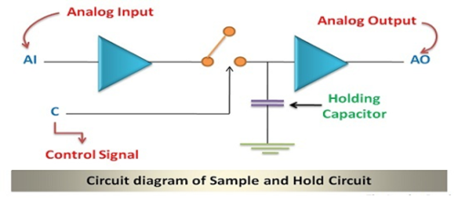
Fig 14 Sample and Hold Circuit
Working of Sample and Hold Circuit
The working of sample and hold circuit can be easily understood with the help of working of its components. The main components which a sample and hold circuit involves is an N-channel Enhancement type MOSFET, a capacitor to store and hold the electric charge and a high precision operational amplifier.
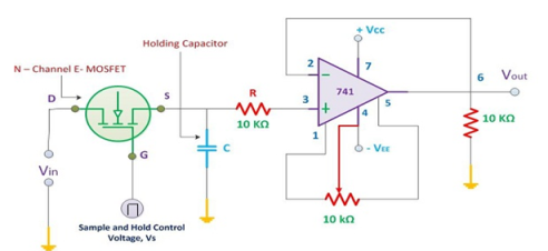
Fig 15 S/H circuit
The N-channel Enhancement MOSFET will be used a switching element. The input voltage is applied through its drain terminal and control voltage will be applied through its gate terminal. When the positive pulse of the control voltage is applied, the MOSFET will be switched to ON state. And it acts as a closed switch. On the contrary, when the control voltage is zero then the MOSFET will be switched to OFF state and acts as the open switch.
When the MOSFET acts as a closed switch, then the analogue signal applied to it through the drain terminal will be fed to the capacitor. The capacitor will then charge to its peak value. When the MOSFET switch is opened, then the capacitor stops charging. Due to the high impedance operational amplifier connected at the end of the circuit, the capacitor will experience high impedance due to this it cannot get discharged.
This leads to the holding of the charge by the capacitor for the definite amount of time. This time can be referred as holding period. And the time in which samples of the input voltage is generated is called sampling period.
The output processed by operational amplifier during the holding period. Therefore, holding period holds significance for OP-AMPS.
Key takeaway
They are used in
- Data Distribution System
- Sampling Oscilloscopes
- Data Conversion System
- Digital Voltmeters
- Analog Signal Processing
- Signal Constructional Filters
Quantizing is defined as the transformation of a continuous analog input into a set of discrete output states. Quantization noise is a model of quantization error introduced by quantization in the analog-to-digital conversion (ADC). It is a rounding error between the analog input voltage to the ADC and the output digitized value. The noise is non-linear and signal-dependent.
An analog-to-digital converter is an electronic device that converts an analog voltage to a digital code. The output of the A/D converter can be directly interfaced to digital devices such as microcontrollers and computers. The resolution of an A/D converter is the number of bits used to digitally approximate the analog value of the input. The number of possible states N is equal to the number of bit combinations that can be output from the converter:
N=2n
Where n is the number of bits. For the example illustrated in Figure, the 3-bit device has 23 or 8 output states as listed in the first column. The output states are
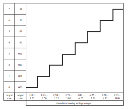
Fig 16 A/D conversion
Usually numbered consecutively from 0 to (N- 1). The corresponding code word for each output state is listed in the second column. Most commercial A/D converters are 8-, 10-, or 12-bit devices that resolve 256, 1024, and 4096 output states, respectively. The number of analog decision points that occur in the process of quantizing is (N- 1). In Figure above, the decision points occur at 1.25 V, 2.50 V, . . . , and 8.75 V. The analog quantization size Q, sometimes called the code width, is defined as the full-scale range of the A/D converter divided by the number of output states
Q=(Vmax-Vmin)/N
It is a measure of the analog change that can be resolved by the converter. Although the term resolution is defined as the number of output bits from an A/D converter, sometimes it is used to refer to the analog quantization size. For our example, the analog quantization size is 10/8 V 1.25 V. This means that the amplitude of the digitized signal has an error of at most 1.25 V. Therefore, the A/D converter can only resolve a voltage to within 1.25 V of the exact analog voltage.
Key takeaway
Quantizing is defined as the transformation of a continuous analog input into a set of discrete output states. Quantization noise is a model of quantization error introduced by quantization in the analog-to-digital conversion (ADC). It is a rounding error between the analog input voltage to the ADC and the output digitized value. The noise is non-linear and signal-dependent.
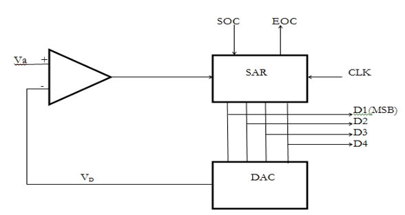
Fig 17 Block Diagram of Successive ADC
1) Successive approximation is one of the most widely and popularly used ADC technique. It uses an efficient “code search” strategy to complete n-bit conversion in just n-clock periods. Thus, it takes much shorter conversion time than counter type ADC.
2) Figure 1 shows the block diagram of successive approximation DAC. A four-bit converter would require eight clock pulses to obtain a digital output.
3) To start conversion “SOC” input is made 1. As soon as “SOC” input is 1, SAR will set MSB to 1 and all other bits to 0 so that trial code output of SAR is D1, D2, D3, D4 = 1000.
4) The output of SAR is then applied to DAC. The corresponding output DAC VDVD is applied to comparator.
5) If VDVD< VaVa i.e., trial code is less than the correct digital representation then output goes high which is applied to SAR.
6) In response to high comparator output, MSB D1 is maintained at 1 and the next bit D2 is made 1. The trial code at the SAR output now becomes 1100. The corresponding DAC output is compared with VaVa and the process continues.
7) However, for the first trial code, VDVD>VaVa, then the comparator output will go low i.e., 0. The SAR will respond to it by reseting its MSB bits D1 to 0 and next bit D2=1 so that the new trial code is 0100.
8) The procedure is repeated for all the subsequent bit one at a time, until all bit position is tested. When all the bit positions are tested, end of conversion (EOC) output goes high to indicate conversion is over.
9) The complete conversion sequence for 4-bit successive approximation ADC is shown in Figure 2. It can be seen that the DAC output voltage becomes successively closer to the actual analog input voltage. It requires n pulses equivalent to n bits to establish the accurate output regardless of the value of the analog input.
Advantages:
- The conversion time is equal to “n” clock cycle period for n-bit ADC. Thus, conversion time is very short for example, for 12-bit ADC with clock frequency of 1MHz, the conversion time will be 12×1µs=12µs only.
- Conversion time is constant and independent of the amplitude of analog signal Va.
Disadvantages:
- The conversion time is more as compared to flash type ADC.
Applications:
- Microprocessor based data acquisition system. IC ADC0809 uses the concept of successive approximation.
Key takeaway
Successive approximation is one of the most widely and popularly used ADC technique. It uses an efficient “code search” strategy to complete n-bit conversion in just n-clock periods. Thus, it takes much shorter conversion time than counter type ADC.
The R-2R resistor ladder network directly converts a parallel digital symbol/word into an analog voltage. Each digital input (b0, b1, etc.) adds its own weighted contribution to the analog output. This network has some unique and interesting properties.
- Easily scalable to any desired number of bits
- Uses only two values of resistors which make for easy and accurate fabrication and integration
- Output impedance is equal to R, regardless of the number of bits, simplifying filtering and further analog signal processing circuit design
The application and advantages are
- It integrates mechanical system with electronic and computer systems.
- It improves efficiency of the system
- It reduces cost of production
- To improve precision and accuracy
- Customer satisfaction and comfort
A typical Media centre consists of a television, a receiver with its speakers, and a cable or satellite box.
● The User interacts with the media centre using a remote control with the capabilities of turning on or off the system, changing the channel, volume and input (i.e., Cable, DVD player, etc.).
● A media centre will almost certainly have many more functions, however, these are the ones absolutely required for use.
Pressure gauge are the sensors which measure the pressure of any process. A pointer which indicates the change in pressure of the process. They indicate absolute pressure depending on the reference pressure. The pressure difference between two points in a system while pressure is defined relative to full vacuum. The absolute pressure and gauge pressure are related as
Absolute pressure= Gauge pressure + Atmospheric pressure
The unit is pascal. Analogue pressure gauges are not accurate and stability is also not good. Digital pressures gauges are more accurate and easier to read to a higher level of precision than mechanical dial pressure gauges. There is no ambiguity when reading a digital pressure gauge, because unlike analogue dial pressure gauges, there is no parallax error caused by viewing a needle on a dial with limited resolution at different angles.
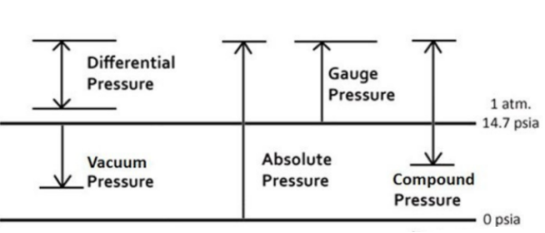
Fig 18 Different types of Pressures
In digital pressure gauge the sensors convert pressure in electronic signals. Piezoelectric sensors are used more frequently as pressure sensors. This sensor consists out of a diaphragm that is equipped with piezoresistive elements. The medium pressure causes the diaphragm to deflect, this deflection causes a change in cross-sectional area of the piezoresistive elements that is directly coupled to the electrical resistance.
Advantages
- The digital pressure gauges have backlighting so that in dark also readings can be taken easily.
- There are many options available so that we set the minimum and maximum readings.
- The display is a bar graph which makes the changes in readings easier to be detected.
- In case of low battery also pressure can be read accurately.
- The display units can be rotated in many of the digital pressure gauges. Making is more user friendly.
Water is now an important factor for mankind. Measuring the supply to all sectors continues to be less important, especially with a constantly growing population. A program of infrastructure development across the country, as well as a statistical measurement of supply, is required. The measurements were carried out using different types of instruments and were also made abroad, using sophisticated technology, and we depend on them for any repairs or maintenance works. The design of a measurement gauging tool (which gives the measurement of the expenditure or water flow that leads to the canal or river). It is an intelligent system that will process the information it receives, providing real-time spending. The system is economical, precise and dynamic. Considering the data acquisition system proposed here the different types of cross-sectional areas of the measurement points, the selection of the type of measuring instrument, determination of the frequency of transmission and communication equipment and the data acquisition technique.
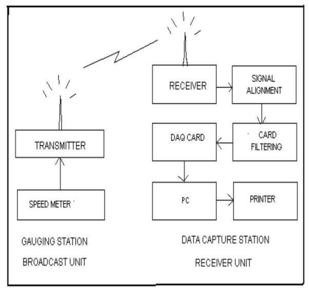
Fig 19 Block Diagram of DAQ System
This type of data acquisition is the sampling of the real world (analog system) to generate data that can be manipulated by a computer or other electronic media (digital). It involves taking a set of physical signals, converting them into electrical voltages and digitizing them, so that they can be processed in a computer.
The signal conditioning interface is a conditioning step, which performs the adaptation of the signal to levels compatible with the element that makes the transformation to a digital signal. The signal reception interface, is responsible for receiving the pulses and by means of a transducer converts an analog output signal and sends the signal to a data acquisition card.
Figure shows a flow chart of the measurement system, where we begin by asking for a key, should you exit the program incorrectly, and if correct then we go to the main menu where you can: measure a capacity, carry out some LV edits or exit the system.
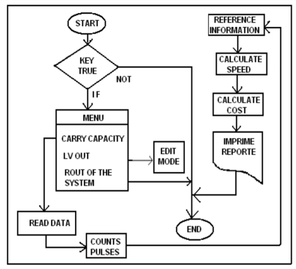
Fig20: Flow diagram of the measurement system.
The Selecting Perform Capacity parameters are introduced, which are required to allow you to start the counting process that begins to store information, and to later make the necessary calculations with the information that was given previously. Thus, ending the process and the results can be printed.
Key takeaway
Water is now an important factor for mankind. Measuring the supply to all sectors continues to be less important, especially with a constantly growing population. A program of infrastructure development across the country, as well as a statistical measurement of supply, is required. The measurements were carried out using different types of instruments and were also made abroad, using sophisticated technology, and we depend on them for any repairs or maintenance works. The design of a measurement gauging tool
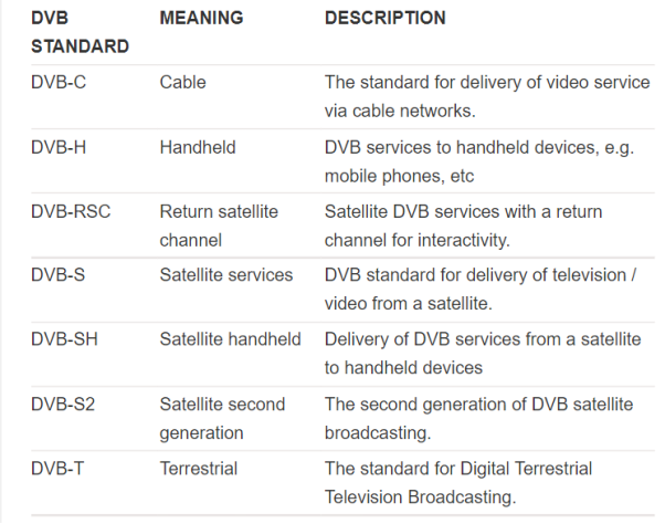
It is being used widely for TV broadcast. There are many advantages of this over the analogue standards. It has taken the television broadcast to much higher level in terms of technology. The DVB is currently implemented by 80 countries around the world. The first of the DVB standards to be agreed was the DVB-S standard for satellite transmission which was agreed in 1994. The DVB system used for terrestrial transmissions, DVB-T was agreed later, in 1997. There are many variants of DVB standards being know till now. There are many ways to transmit and receive signals in television. Only one way is not followed. With DVB being widely used in very many countries, it has now become one of the defacto families of standards for broadcasting. Developments have been made beyond the first DVB standards that were introduced, and now new facilities and levels of performance are being achieved.
The amplitude of the carrier signal varies in accordance with the instantaneous amplitude of the modulating signal. That is the amplitude of the carrier signal containing no information varies as per the amplitude of the signal containing information, at each instant.
Consider the following diagram
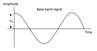
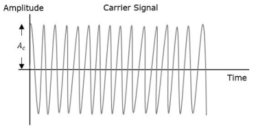
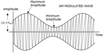
Fig.21: Amplitude Modulation
The first figure shows the modulating wave, which is the message signal. The next one is the carrier wave, which is a high frequency signal and contains no information. While, the last one is the resultant modulated wave.
It can be observed that the positive and negative peaks of the carrier wave are interconnected with an imaginary line. This line helps recreating the exact shape of the modulating signal. This imaginary line on the carrier wave is called as Envelope. It is the same as that of the message signal.
Therefore, we can say that Amplitude Modulation is the process of changing the amplitude of a relatively high frequency carrier signal in accordance with the amplitude of the modulating signal (Information). The carrier amplitude varies linearly by the modulating signal which usually consists of a range of audio frequencies. The frequency of the carrier is not affected.
Time-Domain Representation
Let the modulating signal be,
m(t)=Am cos (2πfmt) --------------(1)
And the carrier signal be,
c(t)=Ac cos(2πfct) c(t) ---------------(2)
Where, Am and Ac are the amplitude of the modulating signal and the carrier signal respectively.
Fm and fc are the frequency of the modulating signal and the carrier signal respectively.
Then, the equation of Amplitude Modulated wave will be
s(t)= [Ac+ Am cos(2πfmt)] cos(2πfct) -------------------------- (3)
s(t) = [ Ac cos(2πfct) + Ac Am cos(2πfmt). Cos(2πfct)] ---------(4)
s(t) = Ac [1 + Am/Ac cos(2πfmt)] cos(2πfct) ----------- (5)
Here the modulation index µ = Am/Ac.
s(t) = Ac [1 + µ cos(2πfmt)] cos(2πfct) -------------- (6)
Modulation index
Let Amax and Amin be the maximum and minimum amplitudes of the modulated wave.
We will get the maximum amplitude of the modulated wave, when cos(2πfmt)
Is 1.
That is Amax=Ac + Am
We will get the minimum amplitude of the modulated wave, when cos(2πfmt)
Is -1.
That is Amin = Ac - Am
Amax + Amin = Ac + Am + Ac –Am = 2Ac
Ac = Amax + Amin/2
Similarly, Amax – Amin = Ac + Am – Ac +Am = 2Am
Am = Amax – Amin /2
Therefore
µ = Amax + Amin
Amax - Amin
Bandwidth:
Bandwidth is the difference between the highest and lowest frequencies of the signal.
BW = fmax – fmin
s(t) = Ac [1+ μcos(2πfmt)] cos(2πfct)
s(t) = Ac cos(2πfct) + Ac μcos(2πfmt) cos(2πfct)
s(t) = Ac cos(2πfct) + Ac μ/2 cos 2π (fc + fm) t + Ac μ/2 cos 2π (fc - fm) t
Hence, the amplitude modulated wave has three frequencies.
- Carrier frequency fc
- Upper sideband frequency fc+fm
- And lower sideband frequency fc−fm
Here, fmax=fc+fm and fmin=fc−fm
BW=fc+fm−(fc−fm)
BW=fc+fm−(fc−fm)
BW=2fm
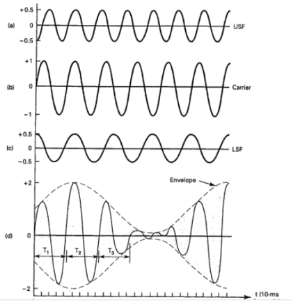
Fig.22: DSBFC
Power Calculation of AM
Consider the following equation of amplitude modulated wave.
s(t)=Ac cos(2πfct) +Acμ 2 cos[2π(fc+fm) t] + Acμ 2cos[2π(fc−fm) t] -------(1)
Power of AM wave is equal to the sum of powers of carrier, upper sideband, and lower sideband frequency components.
Pt=Pc+ PUSB+ PLSB
We know that the standard formula for power is
P = vrms 2 / R = (vm /  ) 2 /2
Where,
Vrms is the rms value of cos signal.
Vm is the peak value of cos signal.
The powers of the carrier, the upper and lower sideband is given by
Carrier power
Pc=(Ac/√2)2/R=Ac2/2R
Upper sideband power
PUSB=(Acμ/2√2)2/R= Ac2 μ2/ 8R
Similarly, for lower sideband power same as that of the upper side band power.
PLSB=(Acμ/2√2)2 /R
PLSB=Ac2μ2/R
Now, let us add these three powers in order to get the power of AM wave.
Pt=Ac2 /2R+Ac2μ2 /8R+Ac2μ2/8R
Pt= Ac2 /2R [ 1+μ2 /4+μ2 /4]
Pt=Pc (1+ μ 2/2)
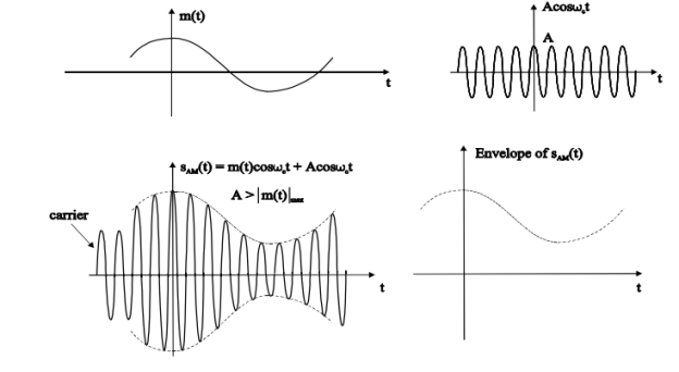
Fig.23: DSBFC
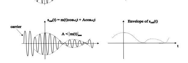
Fig.24: DSBFC
Frequency Modulation
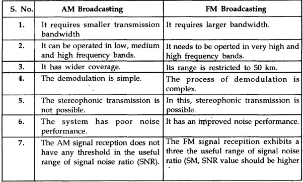
In amplitude modulation, the amplitude of the carrier signal varies, whereas in Frequency Modulation (FM), the frequency of the carrier signal varies in accordance with the instantaneous amplitude of the modulating signal.
Hence, in frequency modulation, the amplitude and the phase of the carrier signal remains constant.
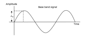
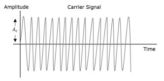
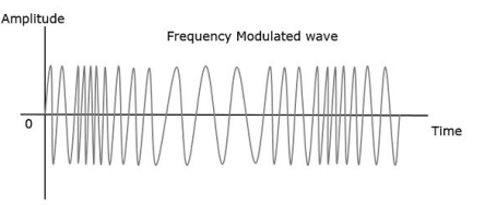
Fig 25 Frequency Modulation
- The frequency fi of the information signal controls the rate at which the carrier frequency increases and decreases. As with AM, fi must be less than fc. The amplitude of the carrier remains constant throughout this process.
- When the information voltage reaches its maximum value then the change in frequency of the carrier will have also reached its maximum deviation above the nominal value.
- Similarly, when the information reaches a minimum, the carrier will be at its lowest frequency below the nominal carrier frequency value.
- When the information signal is zero, then no deviation of the carrier will occur. The maximum change that can occur to the carrier from its base value fc is called the fc. This sets the dynamic range i.e., voltage frequency deviation, of the transmission. The dynamic range is the ratio of the largest and smallest analogue information signals that can be transmitted.
Representation:
The equation for instantaneous frequency fi in FM modulation is
Fi=fc+kfm(t)------------------------(1)
Where,
Fc is the carrier frequency
Kt is the frequency sensitivity
m(t) is the message signal
We know the relationship between angular frequency ωi and angle θi(t) as
ωi=dθi(t)/dt -------------------------(2)
2πfi=dθi(t)dt-------------------------(3)
θi(t)=2π  i dt -------------------------(4)
Substitute, fi value in the above equation.
θi(t)=2π  +k fm(t))dt-----------------(5)
θi(t)=2πfct+2πkf  (t)dt --------------------(6)
This is the equation of FM wave.
If the modulating signal is m(t)=Am cos(2πfmt) then the equation of FM wave will be
s(t)=Ac cos(2πfct+βsin(2πfmt)) -------------------(1)
Where,
β = modulation index =Δf/fm=kfAm/fm----------------------(2)
The difference between FM modulated frequency which is the instantaneous frequency and normal carrier frequency is termed as Frequency Deviation. It is denoted by Δf which is equal to the product of kf and Am.
FM can be divided into Narrowband FM and Wideband FM based on the values of modulation index β.
Key takeaway
References:
- Alciatore & Histand, Introduction to Mechatronics and Measurement system, 4th Edition, Mc-Graw Hill publication, 2011
- Bishop (Editor), Mechatronics – An Introduction, CRC Press, 2006
- Mahalik, Mechatronics – Principles, concepts and applications, Tata Mc-Graw Hill publication, New Delhi
- C. D. Johnson, Process Control Instrumentation Technology, Prentice Hall, New Delhi
- Howard M. B., The 55timer applications sourcebook, with experiments, Indiana, pp. 69, 1980.
- SARH., Instructivo para aforos de corrientes, pp. 98, Mexico, 1957.