Unit 5
Physics of Nano-materials
Nanomaterials are chemical substances or materials that are manufactured and used at a very small scale. Nanomaterials are developed to exhibit novel characteristics compared to the same material without nanoscale features, such as increased strength, chemical reactivity or conductivity.
A natural, incidental or manufactured material containing particles, in an unbound state or as an aggregate or as an agglomerate and where, for 50 % or more of the particles in the number size distribution, one or more external dimensions is in the size range 1 nm - 100 nm.
By derogation from the above, fullerenes, graphene flakes and single wall carbon nanotubes with one or more external dimensions below 1 nm should be considered as nanomaterials.
Nanomaterials that are naturally occurring (e.g., volcanic ash, soot from forest fires) or are generated as incidental (unintentional) by-products of combustion processes (e.g., welding, diesel engines) are usually physically and chemically heterogeneous and often termed ‘ultrafine particles. Engineered nanomaterials, on the other hand, are intentionally produced and designed with physico-chemical properties for a specific purpose or function.
It’s hard to imagine just how smallnanotechnology is. One nanometer is a billionth of a meter, or 10-9 of a meters. Here are a few illustrative examples:
- There are 25,400,000 nanometres in an inch
- A sheet of newspaper is about 100,000 nanometres thick
- On a comparative scale, if a marble were a nanometer, then one meter would be the size of the Earth
Nanoscience and nanotechnology involve the ability to see and to control individual atoms and molecules. Everything on Earth is made up of atoms—the food we eat, the clothes we wear, the buildings and houses we live in, and our own bodies.
But something as small as an atom is impossible to see with the naked eye. In fact, it’s impossible to see with the microscopes typically used in a high school science classes. The microscopes needed to see things at the nanoscale were invented relatively recently—about 30 years ago.
Once scientists had the right tools, such as the scanning tunnelling microscope (STM) and the atomic force microscope (AFM), the age of nanotechnology was born.
Although modern nanoscience and nanotechnology are quite new, nanoscale materials were used for centuries. Alternate-sized gold and silver particles created color in the stained-glass windows of medieval churches hundreds of years ago. The artists back then just didn’t know that the process they used to create these beautiful works of art actually led to changes in the composition of the materials they were working with.
Today's scientists and engineers are finding a wide variety of ways to deliberately make materials at the nanoscale to take advantage of their enhanced properties such as higher strength, lighter weight, increased control of light spectrum, and greater chemical reactivity than their larger-scale counterparts.
Top-Down Methods
Top down methods involve taking a larger bulk material and breaking it up, shearing it, cleaving it and using a significant amount of mechanical, thermal or chemical energy to transform the material into particles in the nanoscale range. In many cases, these methods can be used to create a much higher volume of nanoparticles—and are often used for mass manufacturing—but are often a lot more uncontrollable than bottom-up methods due to the energy or chemical input involved. This can lead to a nanoparticle suspension with a lot higher polydispersity index (i.e. a broader range of nanoparticle sizes) than if the nanoparticles were built from the bottom-up.
Bottom-Up Methods
Bottom-up methods are methods which build up the atomic structure from scratch by depositing atoms under certain conditions to build a desired structure. These are often self-assembly methods. Because the growth often forms periodically, and certain crystal networks are formed as a result, many of these methods are often termed nucleation-growth methods—which stems from the initial formation of an ‘atomic nucleus’ from which the rest of the structure grows from. Whilst there are bottom-up methods which are used to produce nanoparticles commercially, the output is often much lower than top-down methods and is often used for either specific applications or for providing a tailored solution to a problem.
Ball milling (solid-state synthesis) is one of the most important processes used in industry to synthesize nanomaterials, and is also called mechanical alloying or attrition. This method is based on a top-down approach, like self-assembly of molecules and reducing the size of the larger particles. The principle involved in the milling process is the generation of frictional force due to the collision between the reactants’ surface, which leads to increased temperature, pressure, and internal energy
Ultrafine grinding or nanosizing terms were frequently used for the process, when the size of the particle lies in the range of nanometres compared to the other synthesis method. Mechanical attrition methods lead to higher production rates (tons of nanomaterials can be produced in an hour) and widely used in industrial production like metal, clay, and coal powders.
Colloidal nanoparticles are playing a significantly important role in a wide range of fields, including chemistry, material science, physics, engineering, and other interdisciplinary areas due to their interesting optical, chemical, electrical, and physical properties that are very different from their bulk counterparts. Colloidal nanoparticles with controllable size, shape, composition, structure, and crystallinity can fine tune their properties and characterizations based on the required applications. At the nanoscale, the particles possess more surface-to-volume ratio with significantly large portion of the atom residing on the surface compared to the core of the particle. The large amount of surface sites accelerates the adsorption, reaction, and desorption that are favourable for any chemical reaction. Thus, colloidal particles increase the catalytic activity in any of the following methods:
(i) lowering the activation energy of the reaction, (ii) coordinating the reactive species more effectively, and (iii) increasing the production yield when two or more products are formed. Moreover, the decrease in the particle size is not a strict criterion for an increase in the reaction rate per unit catalyst surface area. Benedetti et al. Reported the higher activity for larger palladium nanoparticles for the hydrogenation of 2,4-dinitrotoluene to form 2,4-diaminotoluene because the formation of palladium-b-hydride increases with larger Pd colloidal nanoparticles that control the phase of hydrogenation activity
For the purpose of this article, most current nanomaterials could be organized into four types:
• Carbon Based Materials
• Metal Based Materials
• Dendrimers
• Composites
|
|
Carbon Based Materials These nanomaterials are composed mostly of carbon, most commonly taking the form of a hollow spheres, ellipsoids, or tubes. Spherical and ellipsoidal carbon nanomaterials are referred to as fullerenes, while cylindrical ones are called nanotubes. These particles have many potential applications, including improved films and coatings, stronger and lighter materials, and applications in electronics. Metal Based Materials |
These nanomaterials include quantum dots, nanogold, nanosilver and metal oxides, such as titanium dioxide. A quantum dot is a closely packed semiconductor crystal comprised of hundreds or thousands of atoms, and whose size is on the order of a few nanometers to a few hundred nanometers. Changing the size of quantum dots changes their optical properties.
Dendrimers
These nanomaterials are nanosized polymers built from branched units. The surface of a dendrimer has numerous chain ends, which can be tailored to perform specific chemical functions. This property could also be useful for catalysis. Also, because three-dimensional dendrimers contain interior cavities into which other molecules could be placed, they may be useful for drug delivery.
Composites
Composites combine nanoparticles with other nanoparticles or with larger, bulk-type materials. Nanoparticles, such as nanosized clays, are already being added to products ranging from auto parts to packaging materials, to enhance mechanical, thermal, barrier, and flame-retardant properties.
Microscope,
Scanning Tunnelling Microscope
The development of the family of scanning probe microscopes started with the original invention of the STM in 1981. Gerd Binnig and Heinrich Rohrer developed the first working STM while working at IBM Zurich Research Laboratories in Switzerland. This instrument would later win Binnig and Rohrer the Nobel prize in physics in 1986.
These spatial oscillations are quantum-mechanical interference patterns caused by scattering of the two-dimensional electron gas off the Fe atoms and point defects.
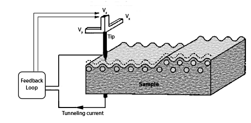
The scanning tunnelling microscope (STM) works by scanning a very sharp metal wire tip over a surface. By bringing the tip very close to the surface, and by applying an electrical voltage to the tip or sample, we can image the surface at an extremely small scale – down to resolving individual atoms.
The STM is based on several principles. One is the quantum mechanical effect of tunnelling. It is this effect that allows us to “see” the surface. Another principle is the piezoelectric effect. It is this effect that allows us to precisely scan the tip with angstrom-level control. Lastly, a feedback loop is required, which monitors the tunneling current and coordinates the current and the positioning of the tip. This is shown schematically below where the tunneling is from tip to surface with the tip rostering with piezoelectric positioning, with the feedback loop maintaining a current setpoint to generate a 3D image of the electronic topography:
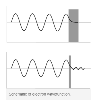
Tunneling is a quantum mechanical effect. A tunneling current occurs when electrons move through a barrier that they classically shouldn’t be able to move through. In classical terms, if you don’t have enough energy to move “over” a barrier, you won’t. However, in the quantum mechanical world, electrons have wavelike properties. These waves don’t end abruptly at a wall or barrier, but taper off quickly. If the barrier is thin enough, the probability function may extend into the next region, through the barrier! Because of the small probability of an electron being on the other side of the barrier, given enough electrons, some will indeed move through and appear on the other side. When an electron moves through the barrier in this fashion, it is called tunneling
Atomic Force Microscope
The atomic force microscope (AFM) was developed to overcome a basic drawback with STM – it can only image conducting or semiconducting surfaces. The AFM has the advantage of imaging almost any type of surface, including polymers, ceramics, composites, glass, and biological samples.
Binnig, Quate, and Gerber invented the AFM in 1985. Their original AFM consisted of a diamond shard attached to a strip of gold foil. The diamond tip contacted the surface directly, with the interatomic van der Waals forces providing the interaction mechanism. Detection of the cantilever’s vertical movement was done with a second tip – an STM placed above the cantilever.
Analogous to how an Scanning Tunneling Microscope works, a sharp tip is raster-scanned over a surface using a feedback loop to adjust parameters needed to image a surface. Unlike Scanning Tunneling Microscopes, the Atomic Force Microscope does not need a conducting sample. Instead of using the quantum mechanical effect of tunneling, atomic forces are used to map the tip-sample interaction.
Often referred to as scanning probe microscopy (SPM), there are Atomic Force Microscopy techniques for almost any measurable force interaction – van der Waals, electrical, magnetic, thermal. For some of the more specialized techniques, modified tips and software adjustments are needed.
In addition to Angstrom-level positioning and feedback loop control, there are 2 components typically included in Atomic Force Microscopy: Deflection and Force Measurement
AFM Probe Deflection
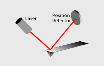
Traditionally, most Atomic Force Microscopes use a laser beam deflection system where a laser is reflected from the back of the reflective AFM lever and onto a position-sensitive detector. AFM tips and cantilevers are typically micro-fabricated from Si or Si3N4. Typical tip radius is from a few to 10s of nm.
Measuring Forces
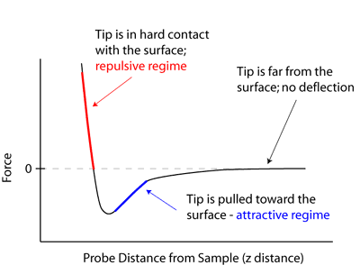
Because the Atomic Force Microscope relies on the forces between the tip and sample, these forces impact AFM imaging. The force is not measured directly, but calculated by measuring the deflection of the lever, knowing the stiffness of the cantilever.
Hooke’s law gives:
F = -kz
Where F is the force, k is the stiffness of the lever, and z is the distance the lever is bent.
Electronic and optical properties
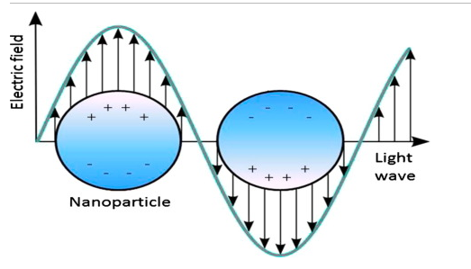
The optical and electronic properties of NPs are inter-dependent to greater extent. For instance, noble metals NPs have size dependent optical properties and exhibit a strong UV–visible extinction band that is not present in the spectrum of the bulk metal. This excitation band results when the incident photon frequency is constant with the collective excitation of the conduction electrons and is known as the localized surface plasma resonance (LSPR). LSPR excitation results in the wavelength selection absorption with extremely large molar excitation coefficient resonance Ray light scattering with efficiency equivalent to that of ten fluorophores and enhanced local electromagnetic fields near the surface of NPs that enhanced spectroscopies.
Magnetic properties
Magnetic NPs are of great curiosity for investigators from an eclectic range of disciplines, which include heterogenous and homogenous catalysis, biomedicine, magnetic fluids, data storage magnetic resonance imaging (MRI), and environmental remediation such as water decontamination. The literature revealed that NPs perform best when the size is <critical value i.e. 10–20 nm. At such low scale the magnetic properties of NPs dominated effectively, which make these particles priceless and can be used in different applications. The uneven electronic distribution in NPs leads to magnetic property. These properties are also dependent on the synthetic protocol and various synthetic methods such as solvothermal, co-precipitation, micro-emulsion, thermal decomposition, and flame spray synthesis can be used for their preparation
Mechanical properties
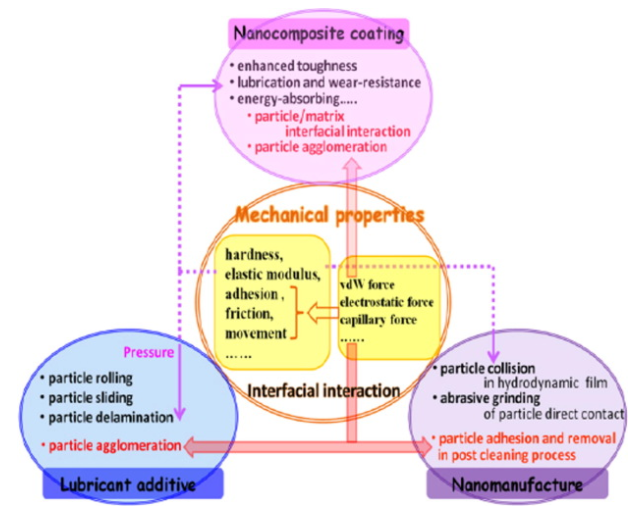
The distinct mechanical properties of NPs allow researchers to look for novel applications in many important fields such as tribology, surface engineering, nanofabrication and nanomanufacturing. Different mechanical parameters such as elastic modulus, hardness, stress and strain, adhesion and friction can be surveyed to know the exact mechanical nature of NPs. Beside these parameters surface coating, coagulation, and lubrication also aid to mechanical properties of NPs. NPs show dissimilar mechanical properties as compared to microparticles and their bulk materials. Moreover, in a lubricated or greased contact, the contrast in the stiffness between NPs and the contacting external surface controls whether the NPs are indented into the plan surface or deformed when the pressure at contact is significantly large.
Thermal properties
It is well-known fact that metals NPs have thermal conductivities higher than those of fluids in solid form. For example, the thermal conductivity of copper at room temperature is about 700 times greater than that of water and about 3000 times greater than that of engine oil. Even oxides such as alumina (Al2O3) have thermal conductivity higher than that of water. Therefore, the fluids containing suspended solid particles are expected to display significantly enhanced thermal conductivities relative to those of conventional heat transfer fluids. Nanofluids are produced by dispersing the nanometric scales solid particles into liquid such as water, ethylene glycol or oils. Nanofluids are expected to exhibit superior properties relative to those of conventional heat transfer fluids and fluids containing microscopic sized particles.
Applications of NPs
In Medicine
NPs have drawn increasing interest from every branch of medicine for their ability to deliver drugs in the optimum dosage range often resulting in increased therapeutic efficiency of the drugs, weakened side effects and improved patient compliance. Iron oxide particles such as magnetite (Fe3O4) or its oxidized form maghemite (Fe2O3) are the most commonly employed for biomedical applications. The selection of NPs for achieving efficient contrast for biological and cell imaging applications as well as for photo thermal therapeutic applications is based on the optical properties of NPs
Applications in manufacturing and materials
Nanocrystalline materials provide very interesting substances for material science since their properties deviate from respective bulk material in a size dependent manner. Manufacture NPs display physicochemical characteristics that induce unique electrical, mechanical, optical and imaging properties that are extremely looked-for in certain applications within the medical, commercial, and ecological sectors. NPs focus on the characterization, designing and engineering of biological as well as non-biological structures < than 100 nm, which show unique and novel functional properties. The potential benefits of nanotechnology have been documented by many manufacturers at high and low level and marketable products are already being mass-produced such as microelectronics, aerospace and pharmaceutical industries
Applications in the environment
The increasing area of engineered NPs in industrial and household applications leads to the release of such materials into the environment. Assessing the risk of these NPs in the environment requires on understanding of their mobility, reactivity, Eco toxicity and persistency. The engineering material applications can increase the concentration of NPs in groundwater and soil which presents the most significant exposure avenues for assessing environmental risks. Due to high surface to mass ratio natural NPs play an important role in the solid/water partitioning of contaminants can be absorbed to the surface of NPs, co-precipitated during the formation of natural NPs or trapped by aggregation of NPs which had contaminants adsorbed to their surface.
Applications in electronics
There has been growing interest in the development of printed electronics in last few years because printed electronics offer attractive to traditional silicon techniques and the potential for low cost, large area electronics for flexible displays, sensors. Printed electronics with various functional inks containing NPs such as metallic NPs, organic electronic molecules, CNTs and ceramics NPs have been expected to flow rapidly as a mass production process for new types of electronic equipment.
Unique structural, optical and electrical properties of one-dimensional semiconductor and metals make them the key structural block for a new generation of electronic, sensors and photonic materials
Applications in energy harvesting
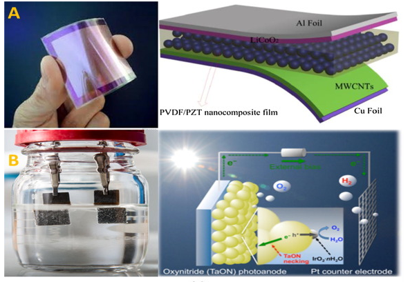
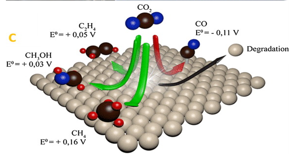
Recent studies warned us about the limitations and scarcity of fossil fuels in coming years due to their non-renewable nature. Therefore, scientists shifting their research strategies to generate renewable energies from easily available resources at cheap cost. They found that NPs are the best candidate for this purpose due to their, large surface area, optical behaviour and catalytic nature. Especially in photocatalytic applications, NPs are widely used to generate energy from photoelectrochemical (PEC) and electrochemical water splitting
