Unit 2
Digital Electronics
The basic gates are namely AND gate, OR gate & NOT gate.
AND gate
It is a digital circuit that consists of two or more inputs and a single output which is the logical AND of all those inputs. It is represented with the symbol ‘.’.
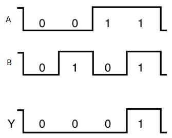
The following is the truth table of 2-input AND gate.
A | B | Y = A.B |
0 | 0 | 0 |
0 | 1 | 0 |
1 | 0 | 0 |
1 | 1 | 1 |
Here A, B are the inputs and Y is the output of two input AND gate.
If both inputs are ‘1’, then only the output, Y is ‘1’. For remaining combinations of inputs, the output, Y is ‘0’.
The figure below shows the symbol of an AND gate, which is having two inputs A, B and one output, Y.

Fig. : AND gate (ref. 1)
Timing Diagram:
OR gate
It is a digital circuit which has two or more inputs and a single output which is the logical OR of all those inputs. It is represented with the symbol ‘+’.
The truth table of 2-input OR gate is:
A | B | Y = A + B |
0 | 0 | 0 |
0 | 1 | 1 |
1 | 0 | 1 |
1 | 1 | 1 |
Here A, B are the inputs and Y is the output of two input OR gate.
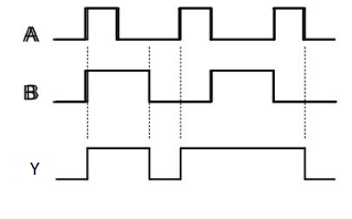
When both inputs are ‘0’, then only the output, Y is ‘0’. For remaining combinations of inputs, the output, Y is ‘1’.
The figure below shows the symbol of an OR gate, which is having two inputs A, B and one output, Y.

Fig. : OR gate (ref. 1)
Timing Diagram:
NOT gate
It is a digital circuit that has one input and one output. Here the output is the logical inversion of input. Hence, it is also called as an inverter.
The truth table of NOT gate is:
A | Y = A’ |
0 | 1 |
1 | 0 |
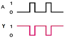
Here A and Y are the corresponding input and output of NOT gate. When A is ‘0’, then, Y is ‘1’. Similarly, when, A is ‘1’, then, Y is ‘0’.
The figure below shows the symbol of NOT gate, which has one input, A and one output, Y.
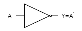
Fig. : NOT gate (ref. 1)
Timing Diagram:
Universal gates
NAND & NOR gates are known as universal gates.
We can implement any Boolean function by using NAND gates and NOR gates alone.
NAND gate
It is a digital circuit which has two or more inputs and single output and it is the inversion of logical AND gate.
The truth table of 2-input NAND gate is:
A | B | Y = (A.B)’ |
0 | 0 | 1 |
0 | 1 | 1 |
1 | 0 | 1 |
1 | 1 | 0 |
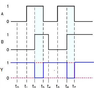
Here A, B are the inputs and Y is the output of two input NAND gate. When both inputs are ‘1’, then the output, Y is ‘0’. If at least one of the input is zero, then the output, Y is ‘1’. This is just the inverse of AND operation.
The image shows the symbol of NAND gate:

Fig.: NAND gate (ref. 1)
NAND gate works same as AND gate followed by an inverter.
Timing Diagram:
NOR gate
It is a digital circuit that has two or more inputs and a single output which is the inversion of logical OR of all inputs.
The truth table of 2-input NOR gate is:
A | B | Y = (A+B)’ |
0 | 0 | 1 |
0 | 1 | 0 |
1 | 0 | 0 |
1 | 1 | 0 |
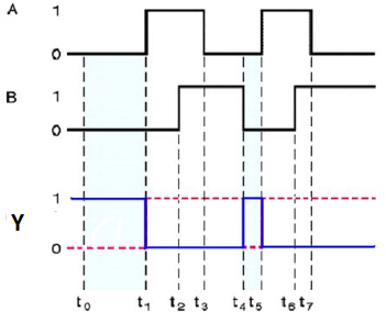
Here A and B are the two inputs and Y is the output. If both inputs are ‘0’, then the output is ‘1’. If any one of the input is ‘1’, then the output is ‘0’. This is exactly opposite to two input OR gate operation.
The symbol of NOR gate is:

Fig.: NOR gate (ref. 1)
NOR gate works exactly same as that of OR gate followed by an inverter.
Timing Diagram:
Special Gates
Ex-OR gate
It stands for Exclusive-OR gate. Its function varies when the inputs have even number of ones.
The truth table of 2-input Ex-OR gate is:
A | B | Y = A⊕B |
0 | 0 | 0 |
0 | 1 | 1 |
1 | 0 | 1 |
1 | 1 | 0 |
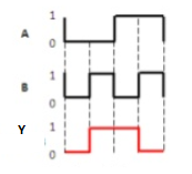
Here A, B are the inputs and Y is the output of two input Ex-OR gate. The output (Y) is zero instead of one when both the inputs are one.
Therefore, the output of Ex-OR gate is ‘1’, when only one of the two inputs is ‘1’. And it is zero, when both inputs are same.
The symbol of Ex-OR gate is as follows:
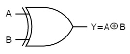
Fig.: XOR gate (ref. 1)
It is similar to that of OR gate with an exception for few combination(s) of inputs. Hence, the output is also known as an odd function.
Timing Diagram:
Ex-NOR gate
It stands for Exclusive-NOR gate. Its function is same as that of NOR gate except when the inputs having even number of ones.
The truth table of 2-input Ex-NOR gate is:
A | B | Y = A⊙B |
0 | 0 | 1 |
0 | 1 | 0 |
1 | 0 | 0 |
1 | 1 | 1 |
Here A, B are the inputs and Y is the output. It is same as Ex-NOR gate with the only modification in the fourth row. The output is 1 instead of 0, when both the inputs are one.
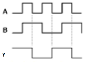
Hence the output of Ex-NOR gate is ‘1’, when both inputs are same and 0, when both the inputs are different.
The symbol of Ex-NOR gate is:
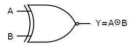
Fig.: XNOR gate (ref. 1)
It is similar to NOR gate except for few combination(s) of inputs. Here the output is ‘1’, when even number of 1 is present at the inputs. Hence is also called as an even function.
Timing Diagram:
Boolean Algebra is used to analyze and simplify the digital (logic) circuits. It uses only the binary numbers i.e. 0 and 1. It is also called as Binary Algebra or logical Algebra. Boolean algebra was invented by George Boole in 1854.
Rule in Boolean Algebra
Following are the important rules used in Boolean algebra.
- Variable used can have only two values. Binary 1 for HIGH and Binary 0 for LOW.
- Complement of a variable is represented by an overbar (-). Thus, complement of variable B is represented as
 . Thus if B = 0 then
  = 1 and B = 1 then
  = 0.
= 0. - ORing of the variables is represented by a plus (+) sign between them. For example ORing of A, B, C is represented as A + B + C.
- Logical ANDing of the two or more variable is represented by writing a dot between them such as A.B.C. Sometime the dot may be omitted like ABC.
Boolean Laws
There are six types of Boolean Laws.
Commutative law
Any binary operation which satisfies the following expression is referred to as commutative operation.

Commutative law states that changing the sequence of the variables does not have any effect on the output of a logic circuit.
Associative law
This law states that the order in which the logic operations are performed is irrelevant as their effect is the same.

Distributive law
Distributive law states the following condition.

AND law
These laws use the AND operation. Therefore they are called as AND laws.

OR law
These laws use the OR operation. Therefore they are called as OR laws.

INVERSION law
This law uses the NOT operation. The inversion law states that double inversion of a variable results in the original variable itself.


A Combinational circuit is a circuit in which we combine the different gates. For example encoder, decoder, multiplexer, demultiplexer etc. Some of the characteristics are as follows −
- The output of combinational circuit depends only on the levels present at input terminals at any instant of time.
- It does not use any memory element. Therefore, the previous state of input does not have any effect on the present state of the circuit.
- It can have n number of inputs and m number of outputs.
Block diagram
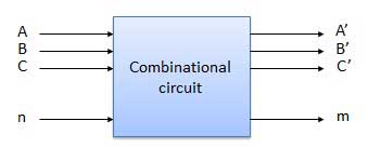
Fig. : Combinational circuit (ref.2 )
It is a combinational circuit which has two inputs and two outputs.
It is designed to add two single bit binary number A and B.
It has two outputs carry and sum.
Block diagram
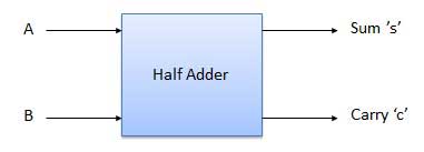
Fig. : Half adder (ref. 2)
Truth Table
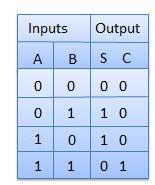
Circuit Diagram
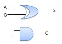
Fig.: Half adder (ref. 2)
Full Adder
It is developed to overcome the drawback of Half Adder circuit.
It can add two one-bit numbers A and B and a carry C.
It is a three input and two output combinational circuit.
Block diagram
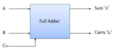
Fig. : Full adder (ref. 2)
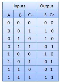
Circuit Diagram
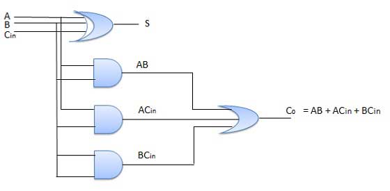
Fig. : Full adder (ref. 2)
Multiplexer and Demultiplexer
Multiplexer means many into one. A multiplexer is a circuit used to select and route any one of the several input signals to a signal output. An simple example of an non electronic circuit of a multiplexer is a single pole multi-position switch.
Multiplexer handle two type of data that is analog and digital. For analog application, multiplexer are built of relays and transistor switches. For digital application, they are built from standard logic gates.
The multiplexer used for digital applications, also called digital multiplexer, is a circuit with many input but only one output. By applying control signals, we can steer any input to the output. Few types of multiplexer are 2-to-1, 4-to-1, 8-to-1, 16-to-1 multiplexer.
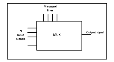
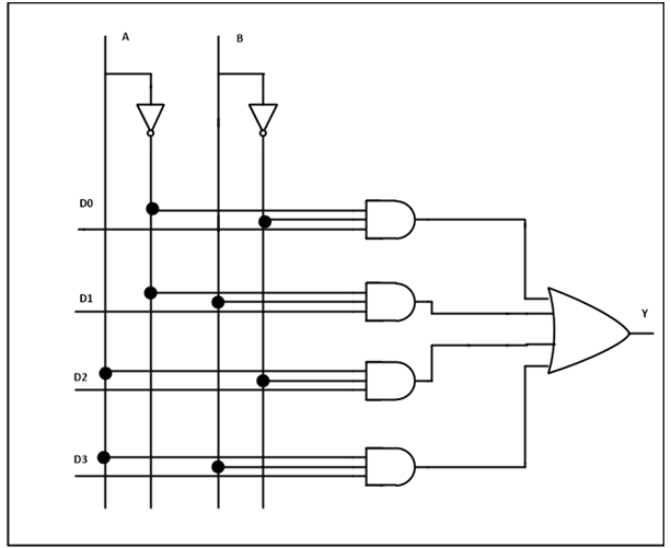
The 4-to-1 multiplexer has 4 input bit, 2 control bits, and 1 output bit. The four input bits are D0,D1,D2 and D3. Only one of this is transmitted to the output y. The output depends on the value of AB which is the control input. The control input determines which of the input data bit is transmitted to the output.
For instance, as shown in fig. When AB = 00, the upper AND gate is enabled while all other AND gates are disabled. Therefore, data bit D0 is transmitted to the output, giving Y = Do.
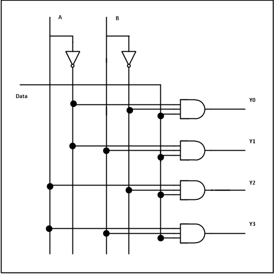
Demultiplexer means one to many. A demultiplexer is a circuit with one input and many output. By applying control signal, we can steer any input to the output. Few types of demultiplexer are 1-to 2, 1-to-4, 1-to-8 and 1-to 16 demultiplexer.
Following figure illustrate the general idea of a demultiplexer with 1 input signal, m control signals, and n output signals.
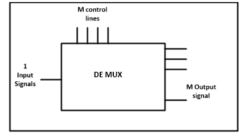
The 1-to-4 demultiplexer has 1 input bit, 2 control bit, and 4 output bits. An example of 1-to-4 demultiplexer is IC 74155. The 1-to-4 demultiplexer is shown in figure below-
References:
- Basic Electrical Engineering” by C L Wadhwa.
- “ Basic Electrical Engineering” by Mehta V K and Mehta Rohit.
- “ Basic Electrical Engineering” by Nagrath, I and Kothari.