UNIT-3
Digital Signalling Formats
Digital Signal formatting is the process of transforming information from one format into another. This is often used in many digital devices and for communication processes. A digital system is a data technology that uses discrete (discontinuous) values. By contrast, non-digital (or analog) systems use a continuous range of values to represent information. Although digital representations are discrete, the information represented can be either discrete, such as numbers, letters or icons, or continuous, such as sounds, images, and other measurements of continuous systems.
One of the simplest ways to transmit digital data is by having a separate clock and data line. In this approach, a clock signal of constant frequency is synchronised with its corresponding data. Depending upon the preference of the designer, the data is either latched on the rising or falling edge of the clock.
NRZ Level itself is not a synchronous system but besides encoding that can be used in either a synchronous or asynchronous transmission environment that is with or without an external clock signal involved in it. Because of that it is not strictly important to discuss how the NRZ-Level encoding act as on a clock edge and during a clock cycle since all transitions happen in the given amount of time represents the actual implied integral clock cycle. The real question is that of sampling the high/low state be received correctly provided the transmission line has stabilized for that bit when the physical line level is sampled at the receiving end.
The binary signal is encoded using rectangular pulse amplitude modulation with polar return-to-zero code
Return-to-zero (RZ) describes a line code used in telecommunications signals in which the signal drops (returns) to zero between each pulse. Returns to zero modulation formats are becoming increasingly popular for long-haul optical fiber transmission systems at bit rates of 10 Gb/s and above.
Previously, the benefits of RZ formats were often overlooked, because they require larger bandwidth than non-return-to-zero (NRZ) formats, and their generation typically requires two cascaded Mach-Zehnder (MZ) modulators. In recent years, it has been shown that RZ can have superior performance over NRZ in certain regimes where chromatic dispersion and fiber nonlinearities are present [2]-[4], as the RZ pulse may exhibit “soliton-like” properties.
In addition, RZ has greater tolerance to polarization-mode dispersion than NRZ Recent research has compared the performance of RZ with different modulation techniques, including binary ON-OFF keying (OOK) and binary differential phase-shift keying (2-DPSK) RZ pulses are frequently generated by driving an MZ modulator by a sinusoidal drive waveform; we assume throughout this paper that RZ pulses are generated in this manner. We define the pulse duty cycle as TFWHM/TS, where TFWHM is the pulsewidth (full-width at half-maximum intensity), and TS is the symbol duration. Depending on the drive waveform amplitude and bias, RZ pulses can have duty cycles of 33%, 50%, and 67%. In particular, 67% RZ is often referred to as carrier-suppressed RZ (CSRZ).
Three factors are considered in selecting phase- and frequency-encode directions: 1) reducing artifacts, 2) minimizing scanning time, and 3) accommodating restrictions imposed by coil design or parallel imaging.
The phase-encoding direction is associated with two major artifacts: wrap-around and flow/motion. Wrap-around (also called aliasing) occurs when the size of the body part imaged exceeds the defined field-of-view (FOV) in the phase-encode direction. This causes anatomy outside the FOV to be folded in over the main part of the image. Although methods exist to overcome this artifact (phase-oversampling) they require additional phase-encoding measurements to be made and hence incur an imaging time penalty. As a rule, therefore, to avoid wrap-around the phase-encoding direction is usually chosen to be along the shortest anatomic dimension. |
The word binary represents two bits. M represents a digit that corresponds to the number of conditions, levels, or combinations possible for a given number of binary variables.
This is the type of digital modulation technique used for data transmission in which instead of one bit, two or more bits are transmitted at a time. As a single signal is used for multiple bit transmission, the channel bandwidth is reduced.
M-ary Equation
If a digital signal is given under four conditions, such as voltage levels, frequencies, phases, and amplitude, then M = 4.
The number of bits necessary to produce a given number of conditions is expressed mathematically as
N=log2M
Where
N is the number of bits necessary
M is the number of conditions, levels, or combinations possible with N bits.
The above equation can be re-arranged as
2N=M
For example, with two bits, 22 = 4 conditions are possible.
Types of M-ary Techniques
In general, Multi-level M−ary modulation techniques are used in digital communications as the digital inputs with more than two modulation levels are allowed on the transmitter’s input. Hence, these techniques are bandwidth efficient.
There are many M-ary modulation techniques. Some of these techniques, modulate one parameter of the carrier signal, such as amplitude, phase, and frequency.
M-ary ASK
This is called M-ary Amplitude Shift Keying M−ASK or M-ary Pulse Amplitude Modulation PAM.
The amplitude of the carrier signal, takes on M different levels.
Representation of M-ary ASK
Sm(t)=Am cos(2πfct) Amϵ(2m−1−M) Δ, m=1, 2....M and0≤t≤Ts
Some prominent features of M-ary ASK are −
- This method is also used in PAM.
- Its implementation is simple.
- M-ary ASK is susceptible to noise and distortion.
M-ary FSK
This is called as M-ary Frequency Shift Keying M−ary FSK.
The frequency of the carrier signal, takes on M different levels.
Representation of M-ary FSK
Some prominent features of M-ary FSK are −
- Not susceptible to noise as much as ASK.
- The transmitted M number of signals are equal in energy and duration.
- The signals are separated by 12Ts12Ts Hz making the signals orthogonal to each other.
- Since M signals are orthogonal, there is no crowding in the signal space.
- The bandwidth efficiency of M-ary FSK decreases and the power efficiency increases with the increase in M.
M-ary PSK
This is called as M-ary Phase Shift Keying M−ary PSK.
The phase of the carrier signal, takes on M different levels.
Representation of M-ary PSK
ϕi(t)=2πiM where i=1,2,3......M
Some prominent features of M-ary PSK are −
- The envelope is constant with more phase possibilities.
- This method was used during the early days of space communication.
- Better performance than ASK and FSK.
- Minimal phase estimation error at the receiver.
- The bandwidth efficiency of M-ary PSK decreases and the power efficiency increases with the increase in M.
So far, we have discussed different modulation techniques. The output of all these techniques is a binary sequence, represented as 1s and 0s.
Bit and Frame Synchronization techniques are used in order to ensure that signals transmitted from one participant of the communication can be correctly decoded by the receiver.
Bit Synchronization
For synchronous transmission, data is not transferred byte-wise so there are no start or stop bits indicating the beginning or end of a character. Instead, there is a continuous stream of bits which have to be split up into bytes. Therefore, the receiver has to sample the received data in the right instant and the sender's and receiver's clocks have to be kept in a synchronized state. As the main task lies in synchronizing sender's and receiver's clocks, bit synchronization is also called clock synchronization.
Clock encoding
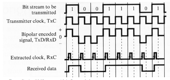
The most self-evident way to accomplish clock synchronization is to send the clock signal to the receiver. This can be done by adding the signal of the local clock to the encoded signal of the bit stream resulting in a bipolar encoded signal which the receiver will have to interpret. By using this bipolar encoding, it is not necessary to create an additional transmission line just for the clock signal. Each bit span of the bipolar2 signal is dived in the middle by the signal shift of the clock. There are two possible values for each bit span: high-zero and low-zero, denoting logical one and logical zero. The received signal will contain enough information for the encoder as it can determine the length of a bit by the guaranteed signal change at the end of each bit and it can determine the literal value by distinguishing between a positive or negative signal in the first half of the bit time
|
Fig.1: Clock encoding
Digital Phase-Locked Loop
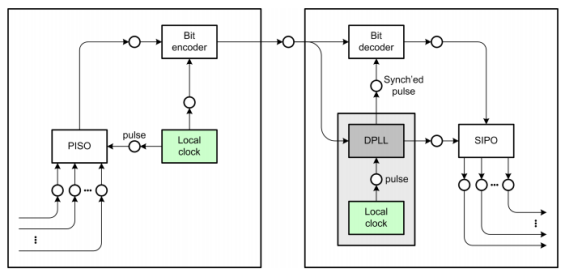
The main idea of a digital phase locked loop is that the receiver's clock is reasonably accurate, but should be resynchronized with the sender's clock whenever possible. Unlike the direct clock encoding, there is no direct transmission of the clock signal, but it is possible to extract clock information from the received data signal. It is important that there are enough bit transitions in the received data stream which indicate bit boundaries and make it possible to deduct the duration of a bit time as well as enabling the clock controller to reset the clock to a less diverged signal. This can be ensured by using a bit scrambler which removes long sequences of zeros or one's, but a more convenient way is to use an encoding scheme which ensures a sufficient number of bit transitions like the Manchester encoding
|
Fig.2: Manchester encoding
Frame synchronization
In modern computer networks data is not transferred as a simple stream of bits or bytes but in terms of frames or packets. This enables amongst other things packet based routing, error correction and the sharing of one physical medium between multiple clients. As the medium usually is a serial link and does not have a concept of frames or separated data units the sender and receiver have to recognize frame borders in the data stream on the medium. This process is called Frame Synchronization.
Time gap synchronization
The most obvious method for synchronization is leaving a time gap between frames. This is of course only possible if an idle state of the transfer medium is recognizable and distinguishable from for example a long row of zeros. If the bits are encoded using return to zero signalling time gaps cannot be used. While this is simple and easy to implement it has disadvantages too. To make sure each of the communication partners recognizes the time gap as such it has to be long enough compared to the length of one information cell in asynchronous data transfers. This brings a performance penalty. Time gap synchronization is usually used in combination with another method of frame synchronization like packet length indication because it might fail if line noise is encountered and by that needs a backup technique.
Start & End Flags
Frame Synchronization via start and end flags is very widely used. The general idea is to separate the single frames by special data sequences, the flags. These flags are commonly referred to as "STX" which stands for "start-of-text" and "ETX" for "end-of text". Whenever the receiver encounters a STX flag it knows it has detected the beginning of a new frame whilst ETX signals the end of the current frame. In many cases there is no need to distinguish between the start and the end of a frame. If the receiver is currently receiving a frame only an ETX character can be valid and if it is not receiving a frame only the STX character can be valid. Because of that to avoid any overhead STX and ETX are usually chosen to be the same character. Please see Figure 19, “Frame Synchronization via start & end flags” for a graphical representation of a frame embedded in STX and ETX flags.
|
Scrambler
Scrambler is a device that transposes or inverts signals or otherwise encodes a message at the sender's side to make the message unintelligible at a receiver not equipped with an appropriately set descrambling device. Whereas encryption usually refers to operations carried out in the digital domain, scrambling usually refers to operations carried out in the analog domain. Scrambling is accomplished by the addition of components to the original signal or the changing of some important component of the original signal in order to make extraction of the original signal difficult. Examples of the latter might include removing or changing vertical or horizontal sync pulses in television signals; televisions will not be able to display a picture from such a signal. Some modern scramblers are actually encryption devices, the name remaining due to the similarities in use, as opposed to internal operation.
Types:
- Additive (synchronous) scramblers
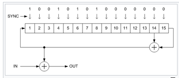
Additive scramblers (they are also referred to as synchronous) transform the input data stream by applying a pseudo-random binary sequence (PRBS) (by modulo-two addition). Sometimes a pre-calculated PRBS stored in the read-only memory is used, but more often it is generated by a linear-feedback shift register (LFSR).
|
- Multiplicative (self-synchronizing) scramblers
Multiplicative scramblers (also known as feed-through) are called so because they perform a multiplication of the input signal by the scrambler's transfer function in Z-space. They are discrete linear time-invariant systems. A multiplicative scrambler is recursive, and a multiplicative descrambler is non-recursive. Unlike additive scramblers, multiplicative scramblers do not need the frame synchronization, that is why they are also called self-synchronizing.
|
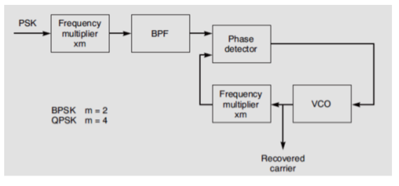
To implement coherent detection, a local oscillator (LO) that is exactly synchronized to the carrier must be provided at the receiver. A BPSK signal is a double sideband suppressed carrier (DSBSC) type of signal e(t) = p(t) cosω0t, and therefore, the carrier is not directly available in the BPSK signal. The carrier can be recovered using a squaring loop, as shown in Fig. Consider first the situation where the input is a BPSK signal. The frequency multiplier is a nonlinear circuit, which squares the signal.
Squaring e(t) results in
|
with p(t)= ±1, the square is just 1. The bandpass filter following the frequency multiplier is tuned to the carrier second harmonic, which provides one of the inputs to the phase detector of the phase-locked loop. The voltage-controlled oscillator (VCO) in the phase-locked loop (PLL) operates at the carrier frequency. The second frequency multiplier provides the second harmonic of this as the other input to the phase detector. The phase difference between these two inputs generates a bias voltage that brings the frequency of the VCO into synchronism with the carrier frequency as derived from the BPSK signal.
|
Fig.5 : Carrier recovery circuit
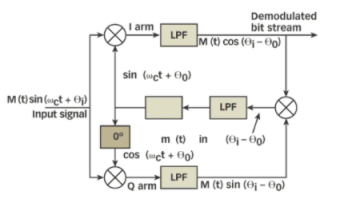
In a BPSK Costas loop, an estimate of carrier phase is obtained by multiplying (with two phase detectors) the input suppressed carrier plus noise with the output of the VCO and a 90-deg.-shifted version of the VCO's signal, respectively, filtering the results of the two multiplications, and using the product of the two filtered signals to control the VCO's phase and frequency. When the filters in the I and Q arms are controlled by integrate-and-dump circuits, the loop is called a Costas loop with active arm filters.
|
Fig.6: Costa’s loop
An optimal phase estimator requires a hyperbolic tangent b/N0)> nonlinearity following the I-arm filter. For large values, tanh(x) equals the polarity or sign of x(±1), and can be implemented with a hard limiter.7 An optimum loop has been practically realized by approximating this hyperbolic tangent nonlinearity.
Costas loop demodulator is an optimal method to attain data and carrier recovery for BPSK signal. It comprises of mixer, low pass filter, phase detector, loop filter and numerically controlled oscillator (NCO). The arm connected to in phase signal is called I channel and one that is connected to quadrature phase signal is called Q channel.
The BPSK modulated signal is multiplied with in phase and quadrature phase carrier signal. They are then passed through LPF where high frequency component are filtered out. The phase detector estimates the phase difference between the two arms of the signals.
The error signal is given to loop filter where it removes the unnecessary spikes. The loop filter controls the phase and frequency of NCO output signal which gives the carrier signal. The demodulated signal is obtained at the output of I-channel.
Phase reversal problem obtained at the output of demodulator can be avoided using differential decoder. Figure 3 shows block diagram of costas loop.
BPSK modulated output is given by m(t) cos(ωc t + θc) - 4
In phase LPF output is given by m(t) cos(θc- θv)
Q- phase LPF output is given by m(t) sin(θc- θv)
PLL is used to lock the carrier phase of modulated signal with the recovered carrier. The recovered carrier will be cos(ωc t).
Squaring loop:
|
Fig7.: Squaring loop
In squaring loop modulated signal is squared, Band Pass Filtered and then multiplied with the carrier that is recovered using PLL to get back base band signal. Although the circuit is simple to implement, it explicits the presence of phase error. Figure shows the block diagram of square loop BPSK demodulator. m(t) be the message signal transmitted.
The BPSK modulated signal is given by A m(t) cos(ωc t + θc). - 1
The squared output is given by A2m 2 (t) cos2 (ωc t + θc).
The BPF output is given by A0cos2(ωc t + θc).
PLL output is given by A0cos2(ωc t + θe).
Frequency divider output is given by A0cos(ωc t + θe)
The recovered carrier output is given by cos(ωc t + θe) - 2
The recovered carrier has phase error of θe
The output of LPF is the demodulated output and is given by A0A m(t)
References:
1. B.P. Lathi, “Modern Digital and Analog communication Systems”, 4th Edition, Oxford University Press, 2010.
2. Rishabh Anand, Communication Systems, Khanna Publishing House, Delhi.
