UNIT - 4
Band pass Modulation & Demodulation
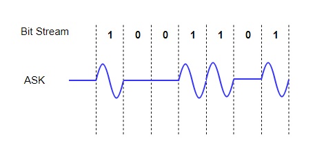
In ASK, the amplitude of the signal is varied to represent the signal levels, while frequency and phase remains constant. In order to represent 0 and 1, two different amplitudes are used.
|
Fig. 1: ASK
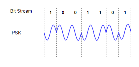
In this, the phase of the carrier signal is modulated to represent the signal levels, while amplitude and frequency remains constant.
Binary Phase Shift Keying (BPSK) is the simplest form of PSK where there are two signal elements represented by two different phases.
In Quadrature PSK (QPSK), two bits of information are transmitted per symbol by using four different phases.
|
Fig. 2: ASK
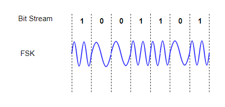
In FSK, the frequency of the signal is modulated to represent the signal levels, while amplitude and phase remains constant.
To represent the signal levels 0 and 1, two different frequencies are used.
|
Fig. 3: ASK
Key Takeaways:
- In ASK, the amplitude of the signal is varied to represent the signal levels, while frequency and phase remains constant.
- In FSK, the frequency of the signal is modulated to represent the signal levels, while amplitude and phase remains constant.
- In PSK, the phase of the carrier signal is modulated to represent the signal levels, while amplitude and frequency remains constant.
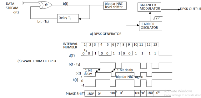
Fig.4: DPSK generation
|
Key Takeaways:
Here, the phase of the modulated signal is shifted relative to the previous signal element. No reference signal is considered here. The signal phase follows the high or low state of the previous element. This DPSK technique doesn’t need a reference oscillator.
GENERATION AND COHERENT DETECTION OF QPSK SIGNALS
(i) Generation
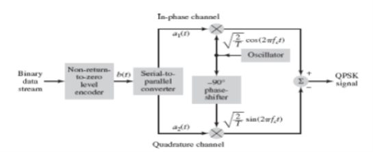
The QPSK Modulator uses a bit-splitter, two multipliers with local oscillator, a 2-bit serial to parallel converter, and a summer circuit.
|
Fig.5: QPSK generation
At the modulator’s input, the message signal’s even bits (i.e., 2nd bit, 4th bit, 6th bit, etc.) and odd bits (i.e., 1st bit, 3rd bit, 5th bit, etc.) are separated by the bits splitter and are multiplied with the same carrier to generate odd BPSK (called as PSKI) and even BPSK (called as PSKQ). The PSKQ signal is anyhow phase shifted by 90° before being modulated.
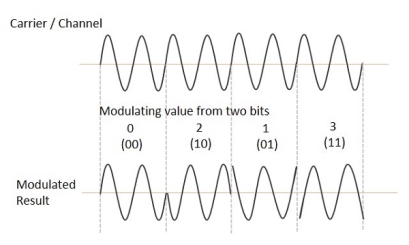
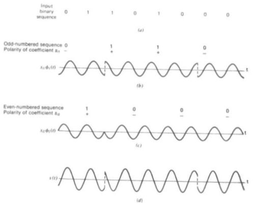
The QPSK waveform for two-bits input is as follows, which shows the modulated result for different instances of binary inputs.
|
Fig.6: QPSK output
(ii) Detection
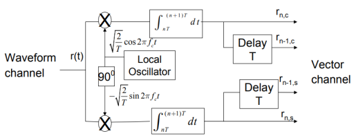
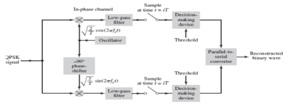
The QPSK Demodulator uses two product demodulator circuits with local oscillator, two band pass filters, two integrator circuits, and a 2-bit parallel to serial converter.
|
Fig.7: QPSK detectors
The two product detectors at the input of demodulator simultaneously demodulate the two BPSK signals. The pair of bits are recovered here from the original data. These signals after processing are passed to the parallel to serial converter.
|
GENERATION AND COHERENT DETECTION OF BPSK SIGNALS
(i) Generation
To generate the BPSK signal, we build on the fact that the BPSK signal is a special case of DSB-SC modulation. Specifically, we use a product modulator consisting of two components.
(i) Non-return-to-zero level encoder, whereby the input binary data sequence is encoded inpolar form with symbols 1 and 0 represented by the constant-amplitude.
(ii) Product modulator, which multiplies the level encoded binary wave by the sinusoidalcarrier of amplitude to produce the BPSK signal. The timing pulses used to generate the level encoded binary wave and the sinusoidal carrier wave are usually, but not necessarily, extracted from a common master clock.
|
(ii) Detection
To detect the original binary sequence of 1s and 0s, the BPSK signal at the channel output is applied to a receiver that consists of four sections
(a)Product modulator, which is also supplied with a locally generated reference signal thatis a replica of the carrier wave
(b)Low-pass filter, designed to remove the double-frequency components of the product modulator output (i.e., the components centered on) and pass the zero-frequency components.
(c)Sampler, which uniformly samples the output of the low-pass filter at where; the localclock governing the operation of the sampler issynchronized with the clock responsible for bit-timing in the transmitter.
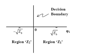
(d)Decision-making device, which compares the sampled value of the low-pass filtersoutput to an externally supplied threshold, every seconds. If the threshold is exceeded, the device decides in favor of symbol 1; otherwise, it decides in favor of symbol 0. levels.
The signal B is
|
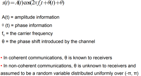
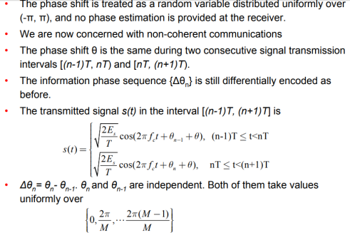
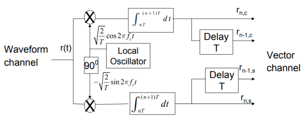
- In coherent communication, - In non coherent communications, - The phase shift is treated as a random variable distributed over - We have now concerned with non coherent communications. - The phase shift is the same during two consecutive signals transmission intervals - The transmission signal s(t) in the interval
ηn.c,ηn.s,ηn-1,c,ηn-1,s are i.i.d
Each of them
|
Operation:
VDPSK(t)=b′(t)∗2Ps−−−√cosωCt VDPSK(t)=b′(t)∗2PscosωCt
VDPSK(t)=VDPSK(t)=b'(t)∗2Ps−−−√cosωCt∗2PscosωCt
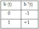
Bt when b(t) =0, b’(t)= -1 hence
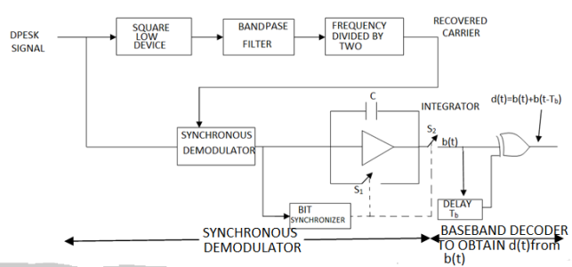
d (t) =0 ………if b(t)=b(t−Tb)(t)=b(t−Tb) And if b(t) = b(t−Tb)b(t−Tb) then output of the EX-OR gate will be 1 d (t) =1 ……… b(t) = b(t−Tb)
|
QAM is a combination of ASK and PSK. Here, both the amplitude and the phase are are varied to transmit more bits per symbol.
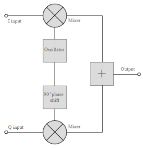
The QAM modulator essentially follows the idea that can be seen from the basic QAM theory where there are two carrier signals with a phase shift of 90° between them. These are then amplitude modulated with the two data streams known as the I or In-phase and the Q or quadrature data streams. These are generated in the baseband processing area.
Basic QAM I-Q modulator circuit
The two resultant signals are summed and then processed as required in the RF signal chain, typically converting them in frequency to the required final frequency and amplifying them as required.
|
Fig.10: Basic QAM
It is worth noting that as the amplitude of the signal varies any RF amplifiers must be linear to preserve the integrity of the signal. Any non-linearities will alter the relative levels of the signals and alter the phase difference, thereby distorting he signal and introducing the possibility of data errors.
Basic QAM I-Q demodulator circuit
The basic modulator assumes that the two quadrature signals remain exactly in quadrature.
A further requirement is to derive a local oscillator signal for the demodulation that is exactly on the required frequency for the signal. Any frequency offset will be a change in the phase of the local oscillator signal with respect to the two double sideband suppressed carrier constituents of the overall signal.
Systems include circuitry for carrier recovery that often utilises a phase locked loop - some even have an inner and outer loop. Recovering the phase of the carrier is important otherwise the bit error rate for the data will be compromised.
|
Fig.11: Basic QAM demodulator
The circuits shown above show the generic IQ QAM modulator and demodulator circuits that are used in a vast number of different areas. Not only are these circuits made from discrete components, but more commonly they are used within integrated circuits that are able to provide a large number of functions.
Key Takeaways:
- Error Probability
|
2. The number of bits necessary to produce a given number of conditions is expressed mathematically as
N=log2M
1. B.P. Lathi, “Modern Digital and Analog communication Systems”, 4th Edition, Oxford University Press, 2010.
2. Rishabh Anand, Communication Systems, Khanna Publishing House, Delhi.
