Need The noise level in the amplifier circuits can be considerably reduced by using negative feedback done by injecting a fraction of output in phase opposition to the input signal. Types of feedback Feedback Amplifiers are classified into: Positive Feedback Amplifier The feedback applied to the input increases the input signal that can be a voltage signal. This is referred to as the positive type. It is also known as a direct amplifier. But these kinds of amplifiers are not good at amplification but can be used in the various types of oscillators. Negative Feedback Amplifier The feedback signal applied to the amplifier if its input signal decreases because of its application. The applied input can be of voltage or current signals. This type of feedback is known as a negative type. It is also referred to as an inverse amplifier. In this case, the noise generated in the circuit is reduced. Hence, it is most widely used in the amplification of the signals. Key Take Aways : The feedback-amplifier can be defined as an amplifier which has feedback lane that exists between output to input. |
Key Take Aways: Feedback reduces the overall gain of a system with the degree of reduction being related to the systems open-loop gain.
|
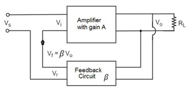
Figure1. Voltage series feedback
In this type of circuit, a portion of the o/p voltage can be applied to the input voltage in series through the feedback circuit. The block diagram of the voltage series feedback-amplifier is shown below. When the feedback circuit is allied in shunt through the output, then o/p impedance will be reduced and i/p impedance is enlarged because of the series connection with the input. As the feedback circuit is connected in shunt with the output, the output impedance is decreased and due to the series connection with the input, the input impedance is increased.
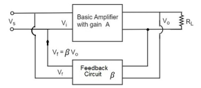
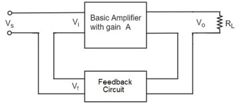
Figure 2.Voltage shunt feedback Figure3. Current series As the feedback circuit is connected in series with the output and the input as well, both the output impedance and the input impedance are increased. When the feedback circuit is allied in series through the o/p in parallel with the input, then the o/p impedance will be increased & because of the parallel connection with the i/p, the i/p impedance will be decreased.
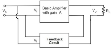
Figure 4: Current Shunt As the feedback circuit is connected in series with the output, the output impedance is increased and due to the parallel connection with the input, the input impedance is decreased. Key Take Away: A Negative-feedback amplifier is an electronic amplifier that subtracts a fraction of its output from its input, so that negative feedback opposes the original signal. |
The important features of Emitter Follower are −
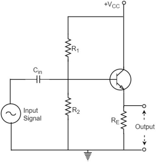
The biasing is provided either by base resistor method or by potential divider method. The following figure shows the circuit diagram of an Emitter Follower.
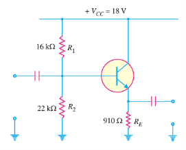
Figure5. Emitter Follower The input signal voltage is applied between base and emitter which develops an output voltage Vo across RE, in the emitter section. Therefore, Vo=IERE ---------------------------(1) The whole of this output current is applied to the input through feedback. Hence, Vf=Vo------------------------------(2) As the output voltage developed across RL is proportional to the emitter current, this emitter follower circuit is a current feedback circuit. Hence, β=VfVo=1----------------------------------(3) The input signal voltage to the transistor (= Vi) is equal to the difference of Vs and Vo i.e., Vi=Vs−Vo---------------------------(4) Problem: For the emitter follower circuit shown in Fig., find VE and IE. Also draw the dc load line for this circuit.
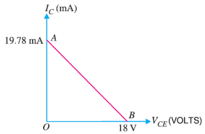
Voltage across R2, V2 = Vcc/R1+R2 xR2 = 18/16+22 x 22 =10.42 V Voltage across RE, VE = V2 – VBE = 10.42 -0.7 = 9.72 V Emitter current IE = VE/RE = 9.72/910 Ω = 10.68mA DC load line Ic(sat) = Vcc/RE = 18/910 = 19.78 mA This locates the point A(OA=19.78mA) of the dc load line VCE (off) =Vcc=18V This locates point B(OB=18V) of the dc load line. By joining points A and B, d.c. load line AB is constructed as shown in figure.
Problem:
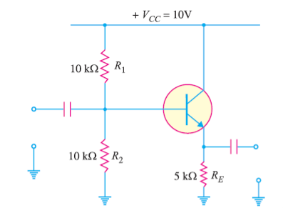
Determine the voltage gain of the emitter follower circuit shown in Figure.
Voltage gain Av = RE/re’+RE Now re’ = 25mV/IE Voltage across R2, V2 = Vcc/R1+R2 x R2 = 10/10+10 x 10 =5V Voltage across RE, VE = V2 -VBE = 5-0.7 =4.3 V Emitter current IE = VE/RE = 4.3 /5k =0.86mA re’ = 25mV/ 0.86mA= 29.1 Ω Voltage gain Av = RE/re’+RE = 5000/ 29.1 +5000 = 0.994
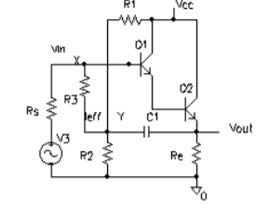
Key Take Aways: The Emitter Follower is used to provide current gain and in impedance matching applications. If IC1=0.1mA Ic2=1mA r2=5K hie=1K and hfe=100 then Re for first stage is 1K+(1+100)5K =506K and VE1 is just 5Kx1mA +0.7 =5.7 V If we had used physical resistance of 500K as Re for first stage and omitted for second stage then Ve1 would have been 500K x 0.1 mA =50V requiring power supply of 100V if Vce=Vre=Vcc/2 . For second stage A12= 1+hfe and R12=(1+fhe) R2 For the first stage load is Ri2 and hoeRi2 is likely to be >0.1 So A11 = (1+hfe)/ (1+hoeR12) = (1+hoe)(1+hfe)R2)=(1+hfe)/(1+hoehfeR2) Overall current gain is A11A12 = (1+hfe) 2 / (1+hoehfeR2) And R1=hie+A12Ri2= (1+hfe)2 R2/ (1+hoehfeR2) R1 for the given parameter is (1+100) 2 x 5K/ (1+25x10-6x100x5K) =50M The Darlington has a drawback that emitter current of first stage is amplified by the current gain of second stage so the first stage drift gets amplified making the circuit drift-prone. The second stage has higher collector current and so the h-parameters of two transistors cannot be considered as same. The effect of bias resistance can be minimised by bootstrapping the CC circuit. Here R1 and R2 are the bias resistances giving base bias through R3. C1 is short circuit the output to point Y at the junction of the bias resistance.
Figure6. Bootstrap At point X the signal voltage is Vin. Let the signal current in R3 be Ieff . Then Ieff = (Vin-Vout) /R3 So the effective resistance of the combination seen by the source is Reff= Vin/Ieff = Vin R3/ (Vin -Vout) = R3/(1-Av) Where Av = voltage gain Vout/Vin
Problem: Two NPN transistors are connected in the form of a Darlington Pair to switch a 12V 75W halogen lamp. If the forward current gain of the first transistor is 25 and the forward current gain (Beta) of the second transistor is 80. Ignoring any voltage drops across the two transistors, calculate the maximum base current required to switch the lamp fully-ON. Firstly, the current drawn by the lamp will be equal to the Collector current of the second transistor, then: Ic = ILAMP ILAMP = P/V = 75/12 = 6.25 Amps Using the equation above, the base current is given as: β1=25 β2=80 Ic = (β1+(β2.β1)+β2).IB IB = Ic/ β1+(β2.β1)+β2 = 6.25/2105 = 3.0mA Key Take Aways: A Darlington Transistor configuration, also known as a “Darlington pair” or “super-alpha circuit”, consist of two NPN or PNP transistors connected so that the emitter current of the first transistor TR1 becomes the base current of the second transistor TR2.
|
References :
- Fundamentals of Analog Circuits (English, Paperback, Floyd Thomas L.)
3. Analog Electronics by J.B Gupta
4. Design with Operational Amplifier and Analog Integrated Circuits by Sergio Franco.
