Consider the block diagram of an audio amplifier and the usage of power amplifier below. Figure 1. Block Diagram of Audio Amplifier Here microphone is used as an input source. The magnitude of signal from the microphone is not sufficient for the power amplifier. So first it is pre-amplified where its voltage and current are increased slightly. Then the signal is passed through tone and volume controls circuit which makes aesthetic adjustments to the audio waveform. Finally, the signal is passed through power amplifier and the output from power amp is fed to a speaker. Key Take Aways: A power amplifier is an electronic amplifier designed to increase the magnitude of power of a given input signal. |
Classification Based on Frequencies Power amplifiers are divided into two categories, based on the frequencies .They are as follows.
Classification Based on Mode of Operation The mode of operation, that is the portion of the input cycle during which collector current flows, the power amplifiers are classified as :
Key Take Aways: Power amplifier circuits are classified as A, B, AB, and C for linear designs—and class D and E for switching designs. The classes are based on the proportion of each input cycle (conduction angle) during which an amplifying device passes current. |
The power drawn from the supply is Pi(dc) = Vcc . ICQ Output Power is given by: Po(ac) = VCE(rms) Ic(rms) Po(ac) = Ic 2 (rms) Rc Po(ac) = Vc 2 (rms) /Rc Efficiency ղ = Po(ac) / Pi(dc) x 100% Key Take Away: There are four factors to be considered output power, gain, operating frequency, and efficiency. |
3.4.1 Harmonic Distortion Harmonic distortion in power amplifiers is mainly caused by the non- linearities of the active elements such as transistors. Non-linearity arises because they are not equally amplified at every point in the input waveform. In different amplifier configurations ClassA has the highest linearity, then class AB, then Class B and finally Class C has the worst linearity. Total Harmonic Distortion is a measure of the number of harmonic components present in a signal. It can be defined as the ratio of the sum of the powers of all the harmonic components to the power of the fundamental frequency. THD is defined as the ratio of the RMS amplitude of the higher order harmonic frequencies to the RMS amplitude of the fundamental frequency. THD is usually expressed in percentage. If V1 is the amplitude of the fundamental frequency and V2, V3, V4……..Vn are the amplitudes of the higher order harmonic frequencies, then THD can be expressed as THD = {√(V2²+V3²+V4²………+Vn²)} / V1----------------------------------(1)
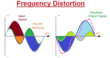
3.4.2 Frequency Distortion Frequency distortion happens when the level of intensification differs with frequency. It happens when large no of inputs which must amplify has a fundamental frequency and a large no of frequencies which called harmonic will distort the original signal.
Figure1. Frequency Distortion
In the figure we can see that input waveforms has a fundamental frequency and second harmonic signal. Their subsequent output wave is shown in the figure at right. The frequency alteration happens when the fundamental frequency syndicates with the second harmonic. By this we can say that Harmonics frequencies are multiples of fundamental Frequency distortion due to harmonics is constantly an option in amplifier circuitries comprising reactive components like capacitor or inductor.
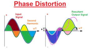
3.4.3Phase Distortion This type of distortion happens in a non-linear amplifier circuit when there is time delay between input and output waves. If we say that the phase change between the input and the output is zero at the fundamental frequency, the subsequent phase angle postponement will be the alteration amid the harmonic and the fundamental frequencies.
Figure2. Phase Distortion Key Take Away: Distortion is a serious problem faced in power amplifier design. In faithful amplification the output signal must be a scaled replica of the input signal and if there is any dissimilarity between the input and output waveform, then the output is said to be distorted. |
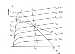
Figure3. Evaluation of Harmonic distortion For a power amplifier with large input swing, it is necessary to express the dynamic transfer curve with respect to the Q point by a power series of the form, Ic = G1ib + G2 i 2b + G3 i3 b ---------------------(1) If the input wave is a simple cosine function of time, then Ib = Ibm cos wt --------------------------------------(2) Then ic = Bo + B1 cos wt + B2 cos 2wt + B3 cos 3wt +-----------------------------(3) Where Bo,B1,B2,B3 are the co-efficient in Fourier series for current that is the total output current is given by ic = I CQ + ic = ICq + B0+B1 coswt + B2 cos2wt +………………(4) Suppose we assume as an approximation that harmonics higher than the fourth are negligible in the above Fourier series, then we have five unknown terms 0, 1 2 3, & 4 To evaluate those, we need output currents at three different value of IB Let us assume that ic=2∆I coswt -----------------------------------------------------(5) Hence IB = IBQ + 2∆i coswt------------------------------------------------------------(6) At wt=0 IB = IBQ + 2∆I ic = Imax --------------------------------------------(7) At wt=π/2 IB= IBQ ic = ICQ ------------------------------------------------(8) At wt=π IB = IBQ -2∆I ic = Imin ----------------------------------------------(9) By combining equations, we get the equations & solving them, we get the following relations, Bo = 1/6 [ Imax+2I1/2 + 2 I-1/2 + Imin] -ICQ ------------------------------------(12) B1 = ¼ [ I max – 2ICQ + I min] -------------------------------------------------------(13) B2 = 1/12 [ Imax -4I1 + 6ICQ – 4I-1/2 + Imin] ------------------------------------(14) The harmonic distortion is defined as D2 = |B1|/|Bo| , D3 =|B2|/|Bo| Where Dn represents the distortion of the nth harmonic. Since this method uses three point on the output waveform to obtain the amplitude of harmonics it is known as three- point method for determining the higher order harmonic distortion. |
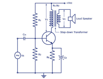
Figure4. Class A Transformer Coupled Amplifier
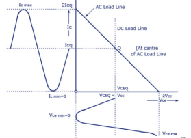
This is also referred to as single ended power amplifier. The term “single ended” denotes only one transistor is used to distinguish it from the push-pull amplifier using two transistors. Operation: When an ac signal is applied to the base of the transistor the collector current will vary around the operating point Q. To get maximum ac power output, the peak value of collector current due to input ac signal alone should be equal to the zero-signal collector current.
To achieve this, the operating point Q is located at the centre of the ac load line by adjusting the biasing circuit (R1, R2 and RE). When ac signal is applied, collector current fluctuates from maximum to minimum (zero), and operating point Q moves up and down the load line. At the peak of the positive half cycle of the input signal, the total collector current Ic max = 2 Ic and collector-emitter – voltage Vcg min = 0 while at the peak of the negative half cycle of the input signal, the collector current Ic min = 0 and collector-emitter voltage Vce max = 2 Vcc. Thus collector-emitter voltage varies in opposite phase to the collector current. The variation of collector voltage appears across primary of the transformer. Now ac voltage is induced in the transformer secondary which in turn develops ac power and supplies to the load.
Figure5. Circuit Operation of Class A amplifier Thus power input to the transistor, Ptr = Power drawn from collector supply, Pin (dc) = VCC ICQ and overall efficiency becomes equal to collector efficiency and = Pout (ac)/ VCC ICQ Under condition of development of maximum ac power, voltage swings from Vce max to zero and collector current from Ic max to zero. So Vrms = 1/√2 { [Vce max – Vce min]/ 2 } = Vce max/2√2 = 2VCC/2√2 = VCC/√2 And Irms = 1/√2 { [Ic max – Ic min]/ 2 } = Ic max/2√2 = 2ICQ/2√2 = ICQ/√2
AC power developed across the load, Pout (ac) = Vrms Irms = (VCC ICQ)/2 Collector efficiency = Pout (ac)/ (VCC ICQ)/2 ÷ VCC ICQ = 0.5 or 50%. Thus, for a transformer-coupled class A power amplifier the maximum theoretical efficiency is 50%. In practice, the efficiency of such an amplifier is somewhat less than 50%. It is about 30%. The efficiency of a transformer-coupled class A power amplifier can be given as Efficiency = 50 *{ [Vce max – Vce min]/ [Vce max + Vce min]} %.
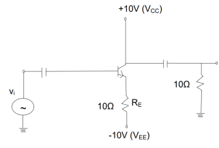
Problem: Calculate maximum ac output power and efficiency of the amplifier shown in fig. VBE may be assumed negligibly small.
The operating point current and voltages in the circuit are: ICQ = IE = |VEE| / RE = 10 V/10 Ω = 1A And VCEQ = Vcc = 10V Therefore, maximum ac output power is Po(max) = VCEQ .ICQ /2 = 10 x ½ = 5W To calculate the efficiency ղ the dc power drawn by collector emitter circuit is PDC = |Vcc| + |VEE| ICQ = (10 + 10) x 1 = 20W Therefore efficiency Ղ = Po(max)/PDC = 5W/20W x 100 = 25%
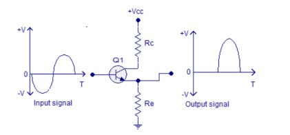
3.6 Class B Amplifier Class B amplifier is a type of power amplifier where the active device (transistor) conducts only for one half cycle of the input signal. That means the conduction angle is 180° for a Class B amplifier. Since the active device is switched off for half the input cycle, the active device dissipates less power and hence the efficiency is improved. Theoretical maximum efficiency of Class B power amplifier is 78.5%. The schematic of a single ended Class B amplifier and input , output waveforms are shown in the figure below. Figure 6. Class B amplifier From the above circuit it is clear that the base of the transistor Q1 is not biased and the negative half cycle of the input waveform is missing in the output. Even though it improves the power efficiency, it creates a lot of distortion. Only half the information present in the input will be available in the output. Single ended Class B amplifiers are not used in present day practical audio amplifier application and they can be found only in some earlier gadgets.
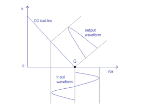
Figure7. Output characteristics of class B amplifier
3.6.1 Class B pushpull amplifier
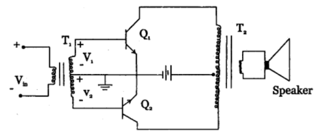
Figure8. Class B push pull amplifier Class B push-pull amplifier is as shown in the diagram. T1 and T2 are two centre tapped transformers and Q1, Q2 are two identical transistors. Transformer T1 produces signal voltages V1 and V2 which are 180° out of phase with each other. These two signals are applied to the Polarities reverse during negative half cycle of input voltage. Q2 then is ON and Q1 is OFF. Q2 amplifies the signal and the alternate half cycle appears across the loud- speaker two transistors. Transformer T2 couples AC output signal from collector to loudspeaker. The two emitters are connected to centre tap of transformer T1 secondary and Vcc to the centre tap of T2 secondary. During positive half cycle of input voltage, secondary winding of T1 has voltages V, and V2. Transistor Q1, conducts and Q2 is cut off. The collector current through Q1 produces an amplified and inverted voltage which applied to loudspeaker through a transformer.
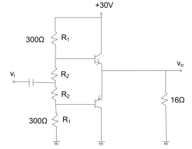
Find out the value of resistor R2 to provide trickle current for distortion free output in the push pull amplifier shown in fig. VBE for each transistor is 0.7V.
Solution Trickle current which flows through resistors R2 and produces a voltage drop of 0.7 V across base – emitter junction over comes cross – over distortion in push – pull amplifier. For analysis purposes, it is sufficient to consider only half of the circuit for reasons of symmetry, and VCC of half (= VCC/2 = 30/2 = 15V) is to be taken for one transistor. I = 15V / R1 + R2 = 15V/ 300Ω + R2 But I x R2 = 0.7V (desired voltage) Or I =0.7 V/R2 -------------------------------------(B) Combining eqs (A) and (B) 0.7 V/R2 = 15/300Ω + R2 R2 = 14.7 Ω
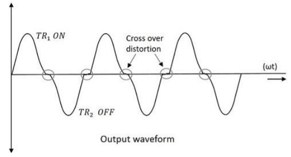
3.6.2 Cross over distortion methods and methods to eliminate cross over distortion. Cross over distortion occurs in Class B push pull Amplifier. * In the push-pull configuration, the two identical transistors get into conduction, one after the other and the output produced will be the combination of both. * When the signal changes or crosses over from one transistor to the other at the zero -voltage point, it produces an amount of distortion to the output wave shape. For a transistor to conduct, the base emitter junction should cross 0.7v, the cut off voltage. The time taken for a transistor to get ON from OFF or to get OFF from ON state is called the transition period. * At the zero- voltage point, the transition period of switching over the transistors from one to the other, has its effect which leads to the instances where both the transistors are OFF at a time. Such instances can be called as Flat spot or Dead band on the output wave shape.
Waveform:-
Figure9. Output Waveform Method to overcome: This cross over distortion can be eliminated if the conduction of the amplifier is more than one half cycle, so that both the transistors won’t be OFF at the same time. The remedy is to use Class AB amplifier.
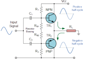
3.6.3 Complimentary symmetry amplifier Figure 10. Symmetry Amplifier Working: The above circuit employs a NPN transistor and a PNP transistor connected in push pull configuration. When the input signal is applied, during the positive half cycle of the input signal, the NPN transistor conducts and the PNP transistor cuts off. During the negative half cycle, the NPN transistor cuts off and the PNP transistor conducts. In this way, the NPN transistor amplifies during positive half cycle of the input, while PNP transistor amplifies during negative half cycle of the input. As the transistors are both complement to each other, act symmetrically while being connected in push pull configuration of class B, this circuit is termed as Complementary symmetry push pull class B amplifier. |
References:
- Fundamentals of Analog Circuits (English, Paperback, Floyd Thomas L.)
3. Analog Electronics by J.B Gupta
4. Design with Operational Amplifier and Analog Integrated Circuits by Sergio Franco.

