Conditions which are required to be satisfied to operate the circuit as an oscillator are called as “Barkhausen criterion” for sustained oscillations. The Barkhausen criterion states that: • The loop gain is equal to unity in absolute magnitude, that is, | β A | = 1 and • The phase shift around the loop is zero or an integer multiple of 2π: ∠ β A = 2 π n, n ∈ 0, 1, 2,…. The product β A is called as the “loop gain”. Key Take Aways: Conditions which are required to be satisfied to operate the circuit as an oscillator are called as “Barkhausen criterion” for sustained oscillations. |
Frequency stability defines the ability of the oscillator to maintain a single fixed frequency as long as it is possible over the time interval. These deviations in frequency are caused due to variations in values of circuit features such as circuit components, transistor parameters, supply voltages, stray-capacitances, output load etc. that determine the oscillator frequency. The amplitude stability measures the amount by which the actual output amplitude varies from desired output amplitude in an oscillator. With the increase in the gain of the amplifier, the amplitude of the waveform is change. Key Take Aways: The term “frequency stability” is used to define the ability of the oscillator to maintain a single fixed frequency as long as possible over a time interval
|
The oscillators are classified as:
Based ON the circuit components:
Based on the range of operating frequency:
Based on whether the feedback is used or not:
Key Take Away: The oscillators are classified based on the nature of the output waveforms, the parameters used, the range of frequency etc. |
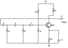
4.4.1 Analysis and Design of RC Phase Shift using BJT RC is known as the collector resistor which stops the transistor’s collector current. The resistor near the transistors like R & R1 form the voltage divider circuit and RE develops the strength. The two capacitors Co & CE, where Co is the o/p DC decoupling capacitor & CE is the emitter bypass capacitor correspondingly. Figure 1. Phase Shift Oscillator using BJT The circuit causes the o/p waveform to move with 180o throughout from the output terminal toward the transistor’s base terminal. Then this signal is moved again with 180o with the help of transistor within the network because of the truth that the phase disparity among the input as well as the output is 180o in the common emitter (CE) configuration. This creates phase disparity to 360 degrees and satisfies the phase disparity condition.
Frequency of RC Phase Shift Oscillator The frequency of RC phase shift oscillator is expressed as f= 1/2πRC√2N Where, R is the Resistance (Ohms) The above frequency formula is used for High Pass Filter related design, and also be used LPF.
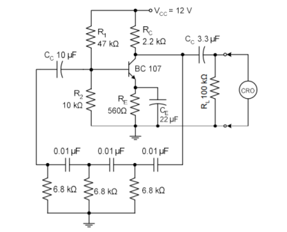
Design: For the given data for BC107 hfe=β=110, Ic max=100mA, Vce max = 45V . Let Vcc =12V, Ic=2mA. Since the quiescent point is in the middle of the load line for the amplifier VCE = 50% of Vcc=6V. VRE= 10% of Vcc =1.2 V. Assume Ic=Ie VRE = Ic RE = IE RE 1.2 = 2 x 10 -3 x RE RE = 1.2 / 2 x 10 -3 = 600Ω The standard value of resistance 560Ω. Voltage across collector resistance V RC = Vcc – VCE – VRE = 12-6-1.2 = 4.8V Rc = VRC/Ic = 4.8 / 2 x 10 -3 = 2.4 kΩ Select 2.2 kΩ Base current IB = Ic/ β = 2 x 10 -3 / 110 = 18.2 μA Take I2 = IB then I1 = 10IB + IB = 11 IB Base Voltage VB = VRE + VBE = 1.2 + 0.6 = 1.8 V R2 = VB/I2 = 1.8 / 10 x 18.2 x 10 -6 = 9.9kΩ Select R2= 10kΩ
Figure 2. Circuit Diagram of RC Phase Shift Oscillator
R1 = Vcc – VB/ I1 = 12-1.8 / 11 x 18.2 x 10 -6 = 51 kΩ
Design of coupling capacitors CC1 and CC2 XC1 should be less than the input impedance of the transistor. Here, Rin is the series impedance. Then Xc1 Here Rin= R1||R2||hfe rE = 47 kΩ||10kΩ||10 x 12.5 Ω = 1.17kΩ We get Rin = 1.17kΩ Then Xc For a lower cut off frequency of 200Hz CC1 = 1/ 2π f Xc1 = 1/2π x 200 x 117 = 6.8 μF Select standard value of 10 μF for CC1 Similarly Xc2 So CC2 = 1/ 2 π f XC2 = 1/ 2π x 200 x 220 = 3.6 μF Select standard value of 3.3 μF for CC2. Design of bypass capacitors CE To bypass the lowest frequency XCE should be much less than or equal to the resistance RE. XCE XCE CE Select standard value of 22 μF for CE.
Design of feedback network The circuit consists of an amplifier stage and a feedback network to provide an additional 180⁰ phase shift, approximately depending upon the frequency of operation. The RC phase shift network must provide 180⁰ or an average of 60⁰ phase shift/lag of RC network. RC phase shift factor k=Vs/Vo For one stage of RC network Vo = IR VC = I Xc tan ɸ = Vc/Vo = IXC / R = 1/ (2πfC) R = 1/2πRC tan ɸ If these are three sections each must give approximately ɸ=60 then tan 60 = √3 f = 1/2πRC √3 In the above phase relationship, between voltage and current in the RC network, the additional current I that flow through C for the other sections so that VC is larger than the value indicated which means that f is smaller than the value obtained in the above equation. A three-stage network would has frequency of oscillation given by f = 1/2πRC √6 Assume f = 1000 Hz and C = 0.01 μF.
Analysis and Design of RC phase shift using FET
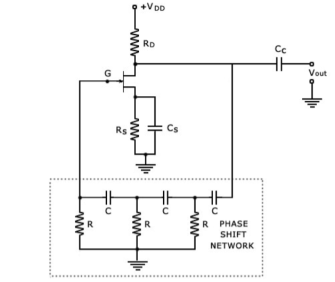
Figure 3. RC Phase Shift Oscillator using FET
The amplifier stage is self- biased with a capacitor bypassed source resistor Rs and a drain bias resistor RD . The FET device parameters of interest are gm and rd. • |A| = gmRL, where RL = (RDrd / RD + rd) • At the operating frequency, the input impedance of the amplifier is infinite. • This is a valid approximation provided, the oscillator operating frequency is low enough so that FET capacitive impedances can be neglected. • The output impedance of the amplifier stage given by RL should also be small compared to the impedance seen looking into the feedback network so that no attenuation due to loading occurs.
Design of RC Phase shift using FET It is desired to design a phase shift oscillator using an FET having gm = 5000µS, rd = 40 kΩ , and a feedback circuit value of R = 10 kΩ. Select the value of C for oscillator operation at 5 kHz and RD for A > 29 to ensure oscillator action.
Solution: f = 1/2√π6RC ; C = 1/2√π6Rf = 1.3nF |A| = gm RL Let A = 40; RL = |A| / gm = 8 kΩ
Key Take Away: The basic RC Oscillator which is also known as a Phase-shift Oscillator, produces a sine wave output signal using regenerative feedback obtained from the resistor-capacitor (RC) ladder network.
|
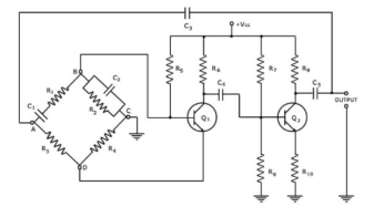
Figure 4. Wein Bridge Oscillator Circuit
The Wien bridge oscillator is used to find the value of unknown values of components. In most of the cases this oscillator is used in the audios. The total phase shift of the oscillator is from the 360° or 0°. The Wein bridge is a two- stage amplifier with RC bridge circuit which has the lead lag networks. The lags at the phase shift are increasing the frequency and the leads are decreasing the frequency. The diagram shows R1 is series with the C1, R3, R4 and R2 are parallel with the C2 to from the four arms. Two transistors are used for the phase shift of 360°and also for the positive feedback. The negative feedback is connected to the circuit of the output with a range of frequencies.
The circuit is in oscillation mode and the base current of the first transistor is changed randomly because of the difference in voltage of DC supply. The base current is applied to the collector terminal of the first transistor and the phase shift is about the 180°. The output of the first transistor is given to the base terminal of the second transistor Q2 with the help of the capacitor C4. Further, this process is amplified and from the second transistor of collector terminal the phase reversed signal is collected. The output signal is connected to the phase with the help of the first transistor to the base terminal. The input point of the bridge circuit is from the point A to point C the feedback of this circuit is the output signal at the second transistor. The feedback signal is given to the resistor R4 which gives the negative feedback. In this same way the feedback signal is given to the base bias resistor R4 and it produces the positive feedback signal. Problem: Determine the RC values of Wien bridge oscillator circuit for the operation at a frequency of 10 kHz if R = 100 K ohms and R1 = 1 K ohm. Given that f = 10 kHz, R = 100 K ohms, R1 = 1K ohm. The frequency of oscillations in Wien bridge oscillator is given as f = 1 / (2πRC) Then C = 1 / (2π × 100 × 103 × 10 × 103)= 0.159nF. For sustained oscillations, gain must be greater than 3, i.e., A ≥ 3 Then 1 + (Rf / R1) ≥ 3 (Rf / R1) ≥ 2 Rf ≥ 1K Ohm Therefore, R and C values are 0.159 nF and 1K Ohm respectively. Key Take Aways: One of the simplest sine wave oscillators which uses a RC network in place of the conventional LC tuned tank circuit to produce a sinusoidal output waveform, is called a Wien Bridge Oscillator. |
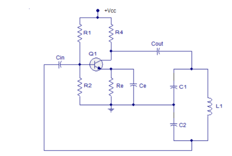
Figure 5. Colpitts oscillator Resistors R1 and R2 work as voltage divider biasing to the transistor. Resistor R4 limits the collector current of the transistor. Cin is the input DC decoupling capacitor while Cout is the output decoupling capacitor. Re is the emitter resistor and its meant for thermal stability. Ce is the emitter by-pass capacitor. Capacitors C1, C2 and inductor L1 forms the tank circuit. The feedback to the base of transistor is taken from the junction of Capacitor C2 and inductor L1 in the tank circuit. When power supply is switched ON, capacitors C1 and C2 starts charging. When fully charged they starts discharging through the inductor L1. When the capacitors are fully discharged, the electrostatic energy stored in the capacitors gets transferred to the inductor as magnetic flux. The inductor starts discharging and capacitors gets charged again. This transfer of energy back and forth between capacitors and inductor is the basis of oscillation. The tank circuit produces 180° phase shift and the transistor itself produces another 180° phase shift. That means the input and output are in phase and it is a necessary condition of positive feedback for maintaining sustained oscillations. The frequency of oscillations of the Colpitts oscillator can be determined using the equation below. f = 1/ 2π√LC where L is the inductance of the inductor in the tank circuit and C is the effective capacitance of the capacitors in the tank circuit.
Problem: A Colpitts Oscillator circuit having two capacitors of 24nF and 240nF respectively are connected in parallel with an inductor of 10mH. Determine the frequency of oscillations of the circuit, the feedback fraction and draw the circuit. The oscillation frequency for a Colpitts Oscillator is given as: fr = 1/ 2π√LCT As the colpitts circuit consists of two capacitors in series, the total capacitance is therefore: CT = 24nF x 240 nF / 24nF + 240nF = 21.82 nF The inductance of the inductor is given as 10mH, then the frequency of oscillation is: fr = 1/ 2π√LCT = 1/ 6.283√0.01 x 21.82 x 10 -9 = 10.8kHz The frequency of oscillations for the Colpitts Oscillator is therefore 10.8kHz with the feedback fraction given as: FF = C1/C2 = 24nF / 240nF = 10% Key Take Aways: The Colpitts oscillator uses a capacitive voltage divider network as its feedback source. 4.6.2 Hartley Oscillator Figure6 . Hartley Oscillator
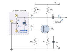
When the circuit is oscillating, the voltage at point X (collector), relative to point Y (emitter), is 180o out-of-phase with the voltage at point Z (base) relative to point Y. At frequency of oscillation, the impedance of the Collector load is resistive and an increase in Base voltage causes a decrease in the Collector voltage. Thus, there is a 180o phase change in the voltage between the Base and Collector and this along with the original 180o phase shift in the feedback loop provides the correct phase relationship of positive feedback for oscillations to be maintained. Resistors, R1 and R2 provide the usual stabilizing DC bias for the transistor in the normal manner while the capacitors act as DC-blocking capacitors. In this Hartley Oscillator circuit, the DC Collector current flows through part of the coil and for this reason the circuit is said to be “Series-fed” with the frequency of oscillation of the Hartley Oscillator being given as. f=1/2π√ LTC where LT = L1 +L2 + 2M Problem: Calculate the frequency of oscillation of Hartley oscillator having L1=0.5mH, L2=1mH and C=0.1μF. F= 1/2π√(L1+L2+2M) C F= 1/2π√(L1+L2) C = 1/2π√(0.5+1) x 10 -3 x 0.2 x 10 -6 Hz =9.19kHz Key Take Aways: The Hartley circuit is often referred to as a split-inductance oscillator because coil L is centre-tapped. |
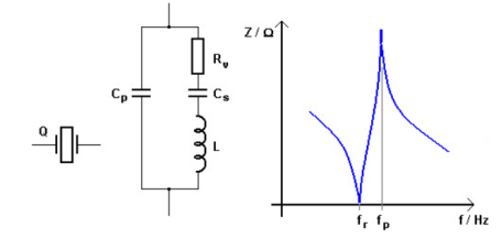
The basic components used in the circuit, inductance L represents crystal mass, capacitance C2 represents compliance, and C1 is used to represent the capacitance that is formed because of crystal’s mechanical moulding, resistance R represents the crystal’s internal structure friction, The quartz crystal oscillator circuit diagram consists of two resonances such as series and parallel resonance, that is two resonant frequencies. Figure 7. Crystal Oscillator Working The series resonance occurs when the reactance produced by capacitance C1is equal and opposite to the reactance produced by inductance L. The fr and fp represents series and parallel resonant frequencies respectively, and the values of ‘fr’ and ‘fp’ can be determined by using the following equations Series resonance fr = 1/2π√L.Cs Parallel Resonance fp = 1/2π√L.Cs . √ 1+Cs/Cp Problem: The series resonating frequency is expressed as fs=(1/2π(√LC)) = 1/2π√(0.4x0.085x10 -12)) =0.856MHz The parallel resonating frequency is given by fp = (1/ (2π √ (LCeq)) The equivalent capacitance under parallel resonance is Ceq = CM C/ CM + C = (0.085 × 1) / (0.085 + 1)=0.078pF fp = (1/ (2π √ (LC)) = (1/ (2π √ (0.4 × 0.078 × 10-12)) = 0.899 MHz The quality factor Q = ws L / R = 2π fs L / R = (2π × 0.856 × 106 × 0.4) / 5 × 10 3 = 430.272 Key Take Away: A crystal oscillator is an electronic oscillator circuit that uses the mechanical resonance of a vibrating crystal of piezoelectric material to create an electrical signal with a constant frequency. |
References:
- Fundamentals of Analog Circuits (English, Paperback, Floyd Thomas L.)
3. Analog Electronics by J.B Gupta
4. Design with Operational Amplifier and Analog Integrated Circuits by Sergio Franco.
