Unit-2
OP-Amp Characteristics
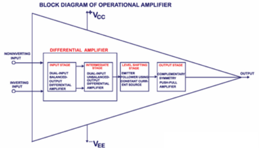
Fig 1 Block Diagram of Operational Amplifier (Op-Amp)
- The op-amp begins with a differential amplifier stage, which operates in the differential mode. Thus the inputs noted with ‘+’ & ‘- ‘ .
- The positive sign is for the non-inverting input and negative is for the inverting input.
- The non-inverting input is the ac signal (or dc) applied to the differential amplifier which produces the same polarity of the signal at the output of op-amp.
- The inverting signal input is the ac signal (or dc) applied to the differential amplifier. This produces 180 degrees out of phase signal at the output.
- The inverting and non-inverting inputs are provided to the input stage which is a dual input, balanced output differential amplifier.
- The voltage gain required for the amplifier is provided in this stage along with the input resistance for the op-amp.
- The output of the initial stage is given to the intermediate stage, which is driven by the output of the input stage.
- In this stage direct coupling is used, which makes the dc voltage at the output of the intermediate stage above ground potential. Therefore, the dc level at its output must be shifted down to 0Volts with respect to the ground.
- For this, the level shifting stage is used where usually an emitter follower with the constant current source is applied.
- The level shifted signal is then given to the output stage where a push-pull amplifier increases the output voltage swing of the signal and also increases the current supplying capability of the op-amp.
Key takeaway:
- The inverting signal input is the ac signal (or dc) applied to the differential amplifier. This produces 180 degrees out of phase signal at the output.
- The inverting and non-inverting inputs are provided to the input stage which is a dual input, balanced output differential amplifier.
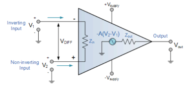
A third terminal represents the operational amplifiers output port which can both sink and source either a voltage or a current.
In a linear operational amplifier, the output signal is the amplification factor, known as the amplifiers gain ( A ) multiplied by the value of the input signal and depending on the nature of these input and output signals, there can be four different classifications of operational amplifier gain.
- Voltage – Voltage “in” and Voltage “out”
- Current – Current “in” and Current “out”
- Transconductance – Voltage “in” and Current “out”
- Transresistance – Current “in” and Voltage “out”
|
Fig 2 Operational Amplifier
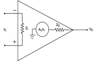
Practical op-amps have zero offset voltage. The bandwidth of the practical op-amp is very small. This output can be raised to the required value by adjusting the negative feedback. The equivalent circuit is shown below.
|
Fig 3 Practical Op-Amp
The input impedance Zi ranges to mega ohms. The output impedance Z0 is in the order of ohms and the practical op-amps have high value of open loop voltage gain AV. The value of CMRR and Slew rate should be as high as possible.
Key takeaway:
For ideal Op-Amp
Open loop gain = 
Input Resistance = 
Output Resistance =0
Offset voltage = 0
Bandwidth of operation = 
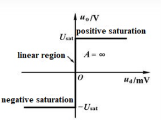
Fig 4 Transfer characteristics of ideal op-amp
Open Loop Gain (Avo)
The main function of an operational amplifier is to amplify the input signal and the more open loop gain it has the better. Open-loop gain is the gain of the op-amp without positive or negative feedback and for such an amplifier the gain will be infinite
Input impedance (ZIN)
Input impedance is the ratio of input voltage to input current and is assumed to be infinite to prevent any current flowing from the source supply into the amplifiers input circuitry ( IIN = 0 ). Real op-amps have input leakage currents from a few pico-amps to a few milli-amps.
Output impedance (ZOUT)
The output impedance of the ideal operational amplifier is assumed to be zero acting as a perfect internal voltage source with no internal resistance so that it can supply as much current as necessary to the load.This internal resistance is effectively in series with the load thereby reducing the output voltage available to the load. Real op-amps have output impedances in the 100-20kΩ range.
Bandwidth (BW):
An ideal operational amplifier has an infinite frequency response and can amplify any frequency signal from DC to the highest AC frequencies, so it is therefore assumed to have an infinite bandwidth.
With real op-amps, the bandwidth is limited by the Gain-Bandwidth product (GB), which is equal to the frequency where the amplifiers gain becomes unity.
Offset Voltage (VIO)
The amplifiers output will be zero when the voltage difference between the inverting and the non-inverting inputs is zero, the same or when both inputs are grounded. Real op-amps have some amount of output offset voltage.
Key takeaway:
High input resistance
Lower output resistance
Infinite voltage amplification
Under a certain supply voltage condition, the amplifier can only work in closed-loop (negative feedback) mode.
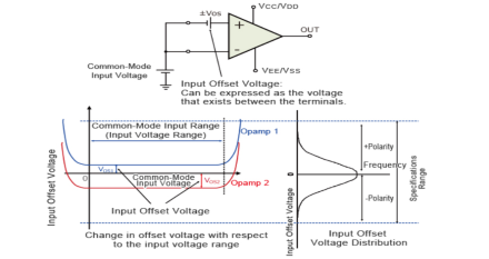
When inputting a common-mode (same) voltage to the input pins of an op-amp or comparator, with an ideal op-amp no output voltage will be output
In case where an input offset voltage exists, a voltage will be output based on the input offset voltage. This input offset voltage, which is the differential voltage required to make the output voltage 0V, becomes the input conversion value.
The Offset voltage is normally expressed in units of mV or µV. Values closer to 0 are more ideal.
|
Fig 4 Op-Amp Parameters
The output offset voltage is the voltage at the output when the differential input voltage is zero.
Key takeaway:
where an input offset voltage exists, a voltage will be output based on the input offset voltage. This input offset voltage, which is the differential voltage required to make the output voltage 0V, becomes the input conversion value.
difference between IB+ and IB-. This difference is called the offset current
|Ios| = IB+-IB------------------------- (7)
Offset current Ios for BJT op-amp is 200nA and for FET op-amp is 10pA. Even with bias current compensation, offset current will produce an output voltage when Vi = 0.
V1 = IB + R comp
And I1 = V1 R1
KCL at node a gives
I2 = (  – I1) =
  - ( Ib + Rcomp/R1 )
Again V0 = I2 Rf – V1
Vo = I2 Rf - IB+ Rcomp
Vo = 1M Ω X 200nA
Vo = 200mV with Vi = 0
Input bias current:
The op-amp‘s input is differential amplifier, which may be made of BJT or FET.
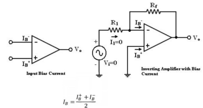
In an ideal op-amp, we assumed that no current is drawn from the input terminals the base currents entering into the inverting and non-inverting terminals (IB- & IB+ respectively).
Even though both the transistors are identical, IB- and IB+ are not exactly equal due to internal imbalance between the two inputs. Manufacturers specify the input bias current IB
|
Fig 5 Input Bias Current Configuration
If input voltage Vi = 0V. The output Voltage Vo should also be (Vo = 0) but for IB = 500nA We find that the output voltage is offset by Op-amp with a 1M feedback resistor
Vo = 500nA X 1M = 500mV
The output is driven to 500mV with zero input, because of the bias currents.
|
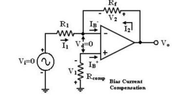
Fig 6 Input Bias Current Compensation
Current IB+ flowing through the compensating resistor Rcomp, then by KVL we get,
- V1+0+V2-Vo = 0 (or)
Vo = V2 – V1 --------- (1)
By selecting proper value of Rcomp, V2 can be cancelled with V1 and the Vo = 0. The value of Rcomp is derived as
V1 = IB+Rcomp (or)
IB+ = V1/Rcomp ------------------------ (2)
The node ‘a’ is at voltage (-V1). Because the voltage at the non-inverting input terminal is (-V1). So with Vi = 0 we get,
I1 = V1/R1 ------------------------ (3)
I2 = V2/Rf ------------------------ (4)
For compensation, Vo should equal to zero (Vo = 0, Vi = 0). i.e. from equation (3) V2 = V1. So that,
I2 = V1/Rf ——> (5)
KCL at node ‘a’ gives,
IB- = I2 + I1 =( V1/Rf ) +(V1/R1) = V1(R1+Rf)/R1Rf ------------------------ (5)
Assume IB- = IB+ and using equation (2) & (5) we get
V1 (R1+Rf)/R1Rf = V1/Rcomp
Rcomp = R1 || Rf ------------------------ (6)
i.e. to compensate for bias current, the compensating resistor, Rcomp should be equal to the parallel combination of resistor R1 and Rf.
Key takeaway
In an ideal op-amp, we assumed that no current is drawn from the input terminals the base currents entering into the inverting and non-inverting terminals. To compensate for bias current, the compensating resistor, Rcomp should be equal to the parallel combination of resistor R1 and Rf.
For example, 1V/us indicates that the voltage can change by 1V in 1us. Ideal op-amps make it possible to faithfully output an output signal for any input signal. However, in reality slew rate limits do exist.
When supplying a rectangular pulse at the input with a steep rise and fall, this indicates the possible degree of change in the output voltage per unit time.
|
Fig 7 Voltage Follower
The rise and fall slew rates are calculated by the following equations:
SRr = ∆ V / ∆ Tr
SRf = ∆ V / ∆ Tf
|
Fig 8 Slew Rate Calculation
Calculate the slew rate
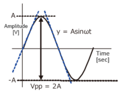
The output is given by
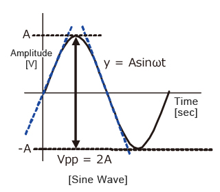
y=Asinωt
The slew rate is the slope of the tangent of the sine wave, differentiating the above equation.
dy | / = Aω cosωt |
| ωt=0 |
Dt |
The slew rate is
SR=Aω ω=2πf
|
Fig 9 Sine wave amplitude
Since the amplitude of the sine wave becomes Vpp=2A (peak-to-peak), the equation can be modified as follows.
|
|
|
|
|
|
|
|
|
This frequency(f) is referred to as the full power bandwidth. These are conditions where the amplification factor in the op-amp has not been set, in other words the relationship of the frequency and amplitude (within the output voltage range) that can be output by the op-amp in a voltage follower circuit.
Key takeaways:
Slew rate is the maximum rate of output voltage change per unit time. It is denoted by S. For getting undistorted output voltage we must have very high slew rate. It is measured in V/sec.
It is the ratio of differential voltage gain Ad to the common mode voltage gain Acm.
CMRR = 
|
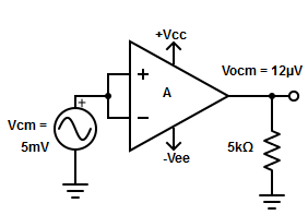
Fig 10 Common Mode Configuration
The common mode voltage gain from above figure can be
 =
= 
Where:
Vocm = output common mode voltage
Vcm = input common mode voltage
Acm = common mode voltage gain
In normal cases the value of Ad is large and Acm is very small making the value of CMRR very high.
Key takeaway:
The common mode voltage gain from above figure can be
 =
= 
PSRR = 
 = Change in input offset voltage
 = Change in supply voltage
It is defined as the change in output offset voltage due to change in temperature. Its unit is  V/0C.
V/0C.
Thermal Drift = 
The thermal drift in input offset current = 
The thermal drift in input bias current = 
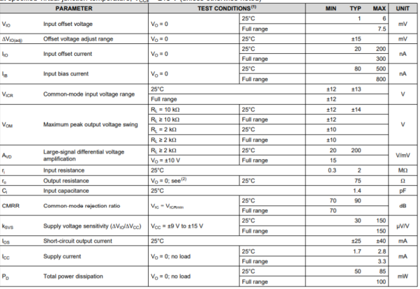
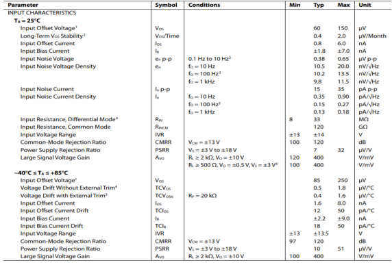
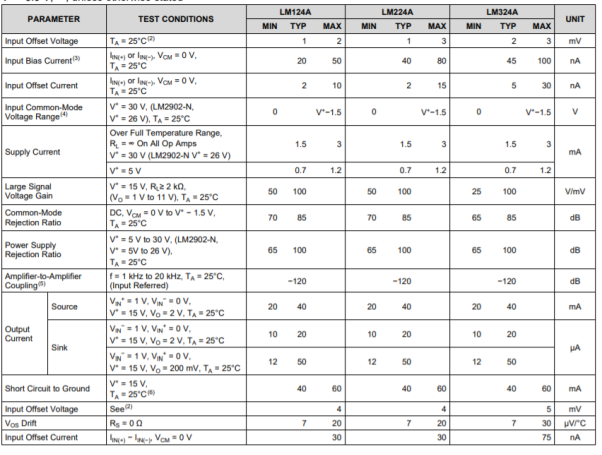
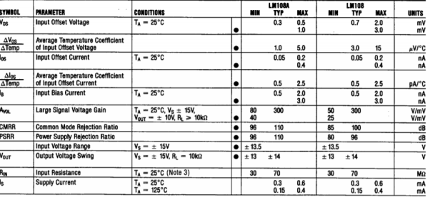
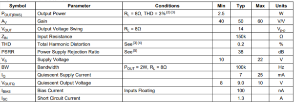
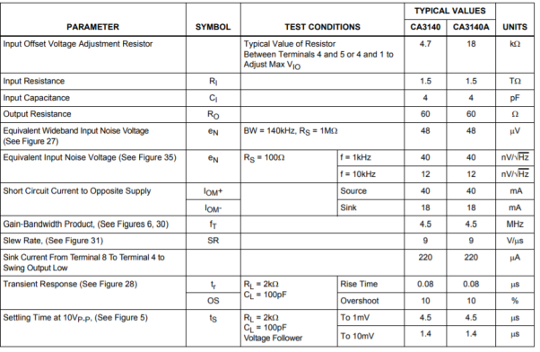
Ref Texas instruments
μA 741
OP7
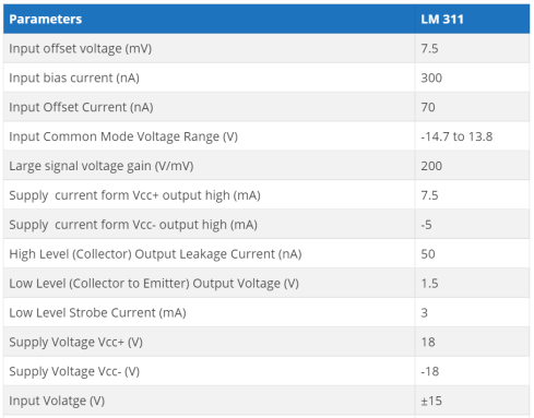
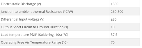
LM 324, LM 311
LM308
LM380
CA 3140
|
References:
1. Ramakant. A. Gayakwad, “Op-Amps & Linear Integrated Circuits”, 3rd Edition, PHI
2. S.Salivahanan&Bhaaskaran, “Linear Integrated Circuits”, 1st Edition, Tata McGraw Hill.
3. T.R Ganesh Babu, “Linear Integrated Circuits”, 3rd Edition, SciTech Publication
4. Sergio Franco, “Design with op-amp &Analog Integrated Circuits”, 3rd Edition, Tata McGraw Hill
