Unit-3
Op-Amp Configurations & Frequency Response
Inverting Amplifier
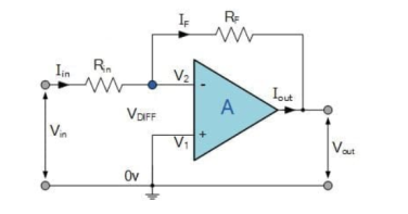
Fig 1 Inverting Amplifier
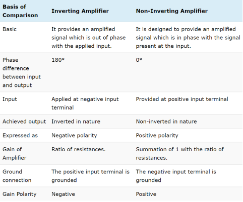
The input signal vi is applied to the inverting input terminal through resistor R1 and non-inverting input terminal is grounded. The feedback from the output of the inverting terminal is provided through the feedback resistor Rf. Since the input is applied to the inverting terminal vo and vi are opposite in polarity and hence the feedback is negative. Since the non-inverting input terminal is grounded v2=0. Due to virtual short at the input of op-amp the inverting and non-inverting input terminals are at the same potential. Therefore, v1 = v2 = 0. Due to high input impedance of Op-amp the current flowing into its inverting input terminal is zero. Therefore, the same current flows through R1 and Rf . i1 = i f But i1 = vi – v1 / R1 = vi/R1 i f = v1 – vo / Rf = -vo/Rf vi/R1 = - vo/Rf Af = vo/vi = -Rf/R1 Af is the closed loop voltage gain or voltage gain with negative feedback.
Example: A 200mV peak to peak sine waveform voltage is applied to Op-amp inverting amplifier with Rf/R1 = 10. Sketch the output. Solution Peak to peak input voltage 2Vm = 200 mV Vm = 100 mV Vi= Vm sin wt = 100 sin wt mV Vo = -Rf/R1 x vi = -10 x 100 sinwt mV = -1000 sin wt mV
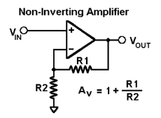
Non-inverting amplifier Non- Inverting amplifier is one in which the output is in phase with respect to input that is if you apply a positive voltage, output will be positive. The output is an non -inverted amplified version of input.
Fig 2 Non-Inverting Amplifier
Assuming the op-amp is ideal and applying the concept of virtual short, the voltage at the inverting terminal is equal to non- inverting terminal. Applying KCL at inverting node we get Vi -Vo/ R2 + Vo – 0 / R1 = 0 By rearranging the terms, we will get
Voltage gain Av = Vo/ Vi = (1+ Rf/Ri)
Gain of non- inverting amplifier Av= (1+ Rf/Ri).
Design a non-inverting amplifier using Op-amp with a closed loop voltage gain of 10. Af = 1 + Rf/R1 =10 Rf/R1 = 9 Rf = 9 R1 If R1 = 1K Rf = 9K Ω
Example-3 In an op-amp inverting amplifier R1 = 1K Ω and Rf = 100KΩ. The DC supply voltage of the op-amp is ± 15V. Calculate the output voltage if input voltage is 1V. R1 = 1KΩ Rf = 100KΩ V+ = 15V and V-=-15V. vi = 1V Af = -Rf/R1 = -100K/1K = -100 Af = vo/vi Vo = Af vi = -100 x 1V = -100V The output voltage cannot exceed the DC power supply voltage. Since vo is negative and large it is limited to V- Vo ≈ V- = -15V
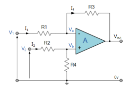
Differential Amplifier The differential amplifier amplifies the difference between two voltages making this type of operational amplifier circuit a Subtractor This type of operational amplifier circuit is commonly known as a Differential Amplifier.
Fig 3 Differential Amplifier
By connecting each input in turn to 0v ground we can use superposition to solve for the output voltage Vout. Then the transfer function for a Differential Amplifier circuit is given as: I1 = V1-Va/R1 ; I2 = V2-Vb/R2 ; If = Va –(Vout)/R3 Summing Point Va =Vb Vb = V2(R4/R2+R4) If V2 =0 then Vout = -V1 (R3/R1) If V1=0 then Vout = V2(R4/R2+R4)(R1+R3/R1) Vout = -Vout (a) + Vout(b) Vout = -V1(R3/R1) + V2(R4/R2+R4)(R1+R3/R1) When resistors, R1 = R2 and R3 = R4 the above transfer function for the differential amplifier can be simplified to the following expression: Vout = (V2 -V1) The output is the difference between the two inputs hence, the op-amp can be used as subtractor. Key takeaways:
|
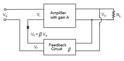
Voltage-Series Feedback The following figure shows the block diagram of voltage series feedback, by which it is evident that the feedback circuit is placed in shunt with the output but in series with the input.
Fig 4 Voltage Series Feedback
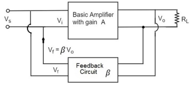
As the feedback circuit is connected in shunt with the output, the output impedance is decreased and due to the series connection with the input, the input impedance is increased. Voltage-Shunt Feedback The below figure shows the block diagram of voltage shunt feedback, by which it is evident that the feedback circuit is placed in shunt with the output and also with the input.
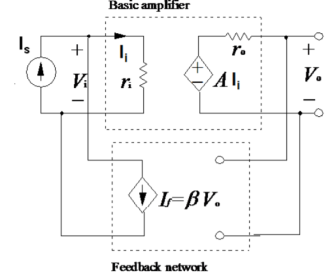
Fig 5 Voltage Shunt Feedback As the feedback circuit is connected in shunt with the output and the input as well, both the output impedance and the input impedance are decreased. Effect on Ri, Ro, gain and bandwidth Voltage shunt feedback amplifier:
Fig 6 Voltage shunt feedback network Voltage gain: Vo =A.Ii = A(Is – If) If = β Vo A(Is – β Vo ) = Vo A Is = (1+βA ) Vo Af = Vo/Is = A/ 1+βA Input Impedance Zin = Vi/Is = Vi/ Ii + If = Ii . ri / Ii + β A Ii Zin = ri / (1+βA) Output Impedance Zout IVS =0 = Vo/Io From input port Ii = -If = - β Vo From output port Io = Vo – A Ii/ro = Vo + βAVo/ro Zo = Vo /Io = ro/ (1+βA)
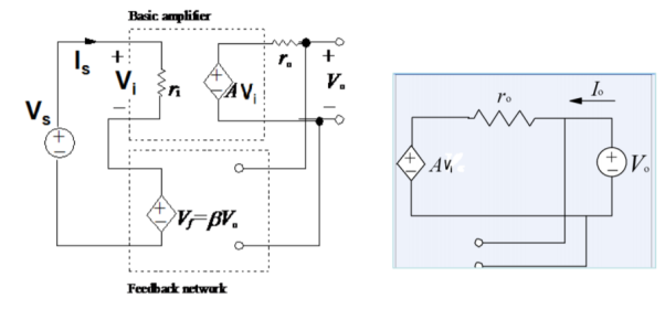
Fig 7 Voltage Series Feedback
Voltage Gain : Vo = A.Vi Vf = β Vo A(Vs – βVo) = Vo AVs = (1+βA) Vo Af = Vo/Vs = A/1+βA
Input impedance Zin = Vs/Is = Vi+βAVi/Is Zin = Vi(1+β A ) /Is = ri(1+βA)
Output Impedance Zout IVS=0 = Vo/Io Io = Vo – A. Vi / ro Vi + β.Vo = Vs Vi = - β Vo Io = Vo + AβVo/ro Zout = Vo/Io = ro / 1+Aβ
Key takeaways:
|
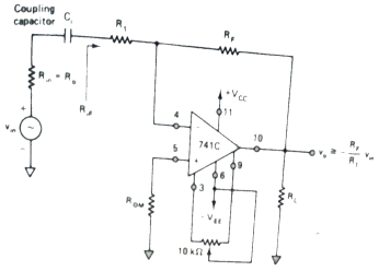
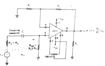
DC amplifiers These amplifiers change their output signal response when experiencing change in its input dc level. A DC amplifier can be inverting, non-inverting or differential. They all are explained broadly in section 3.1. The drawback in using dc amplifiers is that we need to reduce the output offset voltage to zero and this can be achieved by using offset null circuitry. AC amplifiers As AC amplifiers have many applications such as in audio receiver systems. The audio receiver systems experience presence of dc levels at their outputs. These dc levels should not be amplified and to avoid this we use coupling capacitors between the stages. The coupling capacitor blocks dc and also sets the low frequency cut off given as fL = Where: fL =low frequency cut off Ci = dc blocking capacitor Rif = ac input resistance of second stage R0 = ac output resistance of first stage The below figure [Ref.1] shows an ac inverting and ac non-inverting amplifiers.
Fig 8 AC Inverting Amplifier
Fig 9 AC Non-inverting Amplifier
The bandwidth of an amplifier is given as BW =fH-fL The resistor ROM is used to minimise the output offset voltage. The output capacitor C0 can be used in between output terminal of amplifier and the following stage. The coupling capacitor Ci provides low frequency cut off and as it removes the dc level amplification. For ac inverting amplifier the closed loop gain is given as AF = -RF/R1 The closed loop gain of non-inverting amplifier is given as AF = 1+ (RF/R1)
Example-1 From fig 8 shown above [Ref.1] Rin =50Ω, Ci = 0.1μF, R1 =100Ω, RF = 1kΩ, RL =10kΩ and supply voltage of ±15V. Determine the bandwidth of the amplifier? Solution: For inverting amplifier R1= Rif = 100Ω From (1) Rin = R0 = 50Ω fL = The value of fH = (UGB)K/AF AF = -RF/R1 = -1000/100 = -10 fH = (UGB)K/AF = 106 x 0.909/10 = 90.9kHz BW =fH-fL BW = 90.9kHz-10.6kHz = 80.3kHz
Key takeaways The coupling capacitor blocks dc and also sets the low frequency cut off given as fL =
|
Open-loop Frequency Response Curve
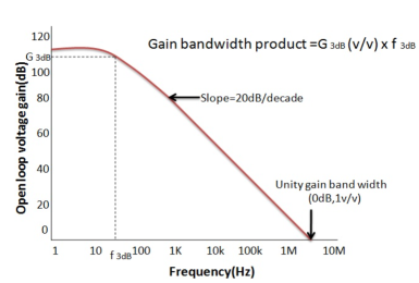
Fig 10 Frequency Response Curve
From this frequency response curve, we can see that the product of the gain against frequency is constant at any point along the curve. Also, that the unity gain (0dB) frequency also determines the gain of the amplifier at any point along the curve. This constant is generally known as the Gain Bandwidth Product or GBP. Therefore: GBP = Gain x Bandwidth = A x BW For example, from the graph above the gain of the amplifier at 100kHz is given as 20dB or 10, then the gain bandwidth product is calculated as: GBP = A x BW = 10 x 100,000Hz = 1,000,000. Similarly, the operational amplifiers gain at 1kHz = 60dB or 1000, therefore the GBP is given as: GBP = A x BW = 1,000 x 1,000Hz = 1,000,000.
The Voltage Gain (AV) of the operational amplifier can be found using the following formula: Av = Vout/ Vin and in Decibels or (dB) is given as: 20 log (A) or 20 log (Vout/ Vin ) in dB
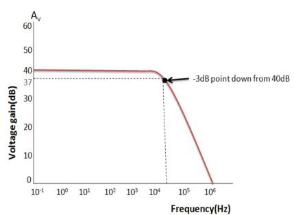
An Op- Amp Bandwidth The operational amplifiers bandwidth is the frequency range over which the voltage gain of the amplifier is above 70.7% or -3dB (where 0dB is the maximum) of its maximum output value.
Fig 11 Frequency Response Example-1 Using the formula 20 log (A), we can calculate the bandwidth of the amplifier as: 37 = 20 log (A) therefore, A = anti-log (37 /20) = 70.8 GBP/ A = Bandwidth, therefore, 1,000,000 / 70.8 = 14,124Hz, or 14kHz Then the bandwidth of the amplifier at a gain of 40dB is given as 14kHz as previously predicted from the graph.
Key takeaways “Open Loop Gain” which is defined as the amplifiers output amplification without any external feedback signals connected to it and for a typical operational amplifier is about 100dB at DC (zero Hz).
|
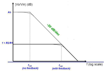
Fig 12 Frequency Response of Op-Amp
The bandwidth of the operational amplifier is defined as the frequency range over which the voltage gain of the amplifier is above -3dB (maximum is 0dB) of its maximum output value. From above curve we see that the product of gain and frequency is constant at any point along the curve. This constant is known as the Gain-Bandwidth product (GB). Also, the gain of the amplifier at any point along the curve is determined by unity-gain (0 dB) frequency. |
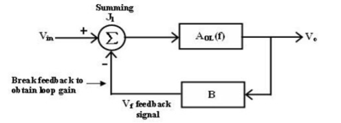
The criterion for stability is used when the system is to be tested practically. In theoretically, always used to test system for stability, ex: Bode plots. Bode plots are compared of magnitude Vs Frequency and phase angle Vs frequency. Any system whose stability is to be determined can represented by the block diagram.
Fig 13 Feedback loop system The block between the output and input is referred to as forward block and the block between the output signal and f/b signal is referred to as feedback block. The content of each block is referred as transfer frequency. From fig. we represented it by AOL (f) which is given by AOL (f) = V0/Vin if Vf = 0 ----- (1) where AOL (f) = open loop volt gain. The closed loop gain Af is given by AF = V0/Vin = AOL / (1+(AOL ) (B) ----(2) B = gain of feedback circuit. B is a constant if the feedback circuit uses only resistive components. Once the magnitude Vs frequency and phase angle Vs frequency plots are drawn, system stability may be determined as follows Method 1: Determine the phase angle when the magnitude of (AOL) (B) is 0dB (or) 1. If phase angle is >-180 Method 2: Determine the phase angle when the magnitude of (AOL) (B) is 0dB (or) 1. If phase angle is > - 180 Key takeaway A system is said to be unstable, if its o/p increases with time instead of achieving a fixed value.
|
For example, 1V/us indicates that the voltage can change by 1V in 1μs. Ideal op-amps make it possible to faithfully output an output signal for any input signal. However, in reality slew rate limits do exist. When supplying a rectangular pulse at the input with a steep rise and fall, this indicates the possible degree of change in the output voltage per unit time.
Fig 14 Slew Rate calculation The rise and fall slew rates are calculated by the following equations: SRr = ∆ V / ∆ Tr SRf = ∆ V / ∆ Tf
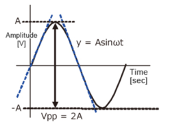
Fig 15 Sinusoidal waveform
Calculate the slew rate The output is given by y=Asinωt The slew rate is the slope of the tangent of the sine wave, differentiating the above equation.
The slew rate is SR=Aω ω=2πf
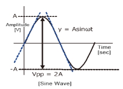
Fig 16 Sinusoidal Waveform
Since the amplitude of the sine wave becomes Vpp=2A (peak-to-peak), the equation can be modified as follows.
This frequency(f) is referred to as the full power bandwidth. These are conditions where the amplification factor in the op-amp has not been set, in other words the relationship of the frequency and amplitude (within the output voltage range) that can be output by the op-amp in a voltage follower circuit. Key takeaway: Slew rate is the maximum rate of output voltage change per unit time. It is denoted by S. For getting undistorted output voltage we must have very high slew rate. It is measured in V/sec.
|
References:
1. Ramakant. A. Gayakwad, “Op-Amps & Linear Integrated Circuits”, 3rd Edition, PHI
2. S.Salivahanan & Bhaaskaran, “Linear Integrated Circuits”, 1st Edition, Tata McGraw Hill.
3. T.R Ganesh Babu, “Linear Integrated Circuits”, 3rd Edition, SciTech Publication
4. Sergio Franco, “Design with op-amp &Analog Integrated Circuits”, 3rd Edition, Tata McGraw Hill
