Unit-4
Linear & Non-Linear Applications
4.1.1 Inverting Summing Amplifier
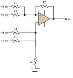
Fig1: Summing amplifier
Hence,
Similarly,
So, the resultant output voltage by all the 4 input voltages is given by,
Vo = V01 + V02 + V04 +V05 Vo = -V1 – V2 +V4 + V5
The output voltage Vo is equivalent to the sum all input voltages applied at both the terminals.
Example 1: In a summing amplifier, if R = 1kΩ, Va = +3V, Vb = +8V, Vc = +9V, Vd = +5V and supply voltage is ±15V. Find the output voltage Vo. Solution: Vo = Sum of all input voltages applied at both the terminals Vo = Va + Vb + Vc +Vd Vo = -3 -8 +9 +5 Vo = +3V
Example 2:
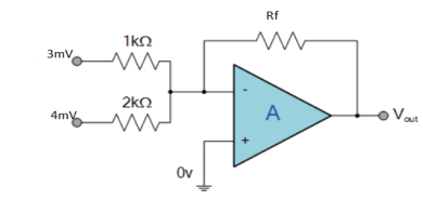
Find the output voltage for the given circuit diagram if Rf = 5kΩ.
Solution: We know, Gain (Av) = Hence, Av1 = Av2 = Now, Output voltage Vo = Sum of the two amplified input signals Vo = Av1 x V1 + Av2 x V2 Vo =(-5 x 3) + ( -2.5x 4) mV Vo = -25mV As the above output voltage is negative hence it is an inverting amplifier.
4.1.2 Non-Inverting
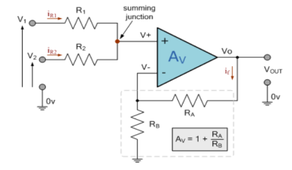
Fig 2: Non-Inverting Summing Amplifier Applying KCL to the above circuit we have IR1+IR2 = 0
When R1 = R2 =R V+ = The voltage gain for non-inverting summing amplifier is given as AV = Vout/Vin = Vout= [1+
Key takeaway: AV = Vout/Vin = Vout= [1+
|
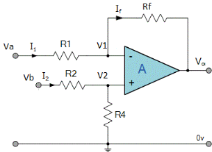
Fig 3: Difference amplifier
Summing point, V1 = V2 and V2 = Vb
If Vb = 0 then
And Va = 0 then
Vo = -V01 + V02
Vo =
If R1 = R2 and Rf = R4 then
And if R1 = R2 = Rf = R4 =R then
Vo = Vb – Va
Hence, is known as a Unity Gain Differential Amplifier.
Key takeaway The output of subtractor is
|
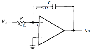
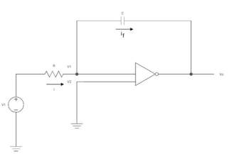
Fig 4: Integrator
Ignoring I3 we have, I3 ≈ 0 So, I1 ≈ I2.
However, V = 0 because gain A is very large
Integrating both sides we get
Where Q is the integration constant and is proportional to Vo at t = 0 sec.
Therefore, voltage Vo is directly proportional to Vin and inversely proportional to constant RC. Frequency response of basic integrator circuit is given by,
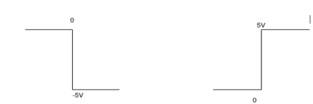
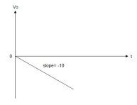
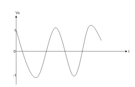
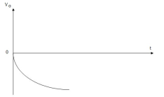
Example-1 The integrator circuit as shown in the figure has R = 500K Ω and C=1µF. Find and plot the output voltage for the inputs as shown in the figure.
a) b) c)vi= 2 sin 4tV d) vi= 4tV
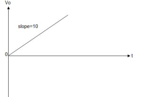
Solution: We know that v0 = - 1/RC Here R= 500K Ω and C = 1µF 1/RC = 1/ 500 x 1000 x 1 x 10-6 = 1/RC = 2 = -2 = -2 = 10t V Which means it is a ramp voltage with positive slope.
When vi=5V -2 = -2 = -10t V Which means it is a ramp voltage with negative slope.
When vi= 2 sin4t V Vo = -2 = -4 [-cos 4t] /4 = cos 4t
When vi=4t V
Vo =
= -8 [t2/2] = - 4V
Key takeaway
Where Q is the integration constant and is proportional to Vo at t = 0 sec.
|
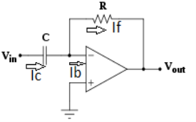
Fig 5: Differentiator
Since Ib = 0 then, Ic ≈ If
Since Gain A is very large hence, V1 = 0
Or
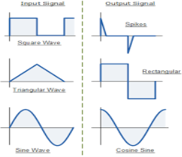
Fig 6: Input and output waveform of differentiator
Frequency response of basic differentiator circuit is given by,
Key takeaway The output voltage for differentiator is
|
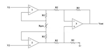
This instrumentation amplifier provides high input impedance for exact measurement of input data from transducers. The circuit diagram of an instrumentation amplifier is as shown in the figure below.
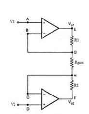
Fig 7 Instrumentation Amplifier The op-amps 1 & 2 are non-inverting amplifiers and together form an input stage of the instrumentation amplifier. The op-amp 3 is a difference amplifier that forms the output stage of the instrumentation amplifier. Working The output stage of the instrumentation amplifier is a difference amplifier, whose output Vout is the amplified difference of the input signals applied to its input terminals. If the outputs of op-amp 1 and op-amp 2 are Vo1 and Vo2 respectively, then the output of the difference amplifier is given by, Vout = (R3/R2)(Vo1-Vo2) The expressions for Vo1 and Vo2 can be found in terms of the input voltages and resistances. Consider the input stage of the instrumentation amplifier as shown in the figure below.
Fig 8 Input Stage of Instrumentation Amplifier The potential at node A is the input voltage V1. Hence the potential at node B is also V1, from the virtual short concept. Thus, the potential at node G is also V1. The potential at node D is the input voltage V2. Hence the potential at node C is also V2, from the virtual short. Thus, the potential at node H is also V2. Ideally the current to the input stage op-amps is zero. Therefore, the current I through the resistors R1, Rgain and R1 remains the same. Applying Ohm’s law between the nodes E and F, I = (Vo1-Vo2)/(R1+Rgain+R1) ——————— 1 I = (Vo1-Vo2)/(2R1+Rgain) Since no current is flowing to the input of the op-amps 1 & 2, the current I between the nodes G and H can be given as, I = (VG-VH)/Rgain = (V1-V2)/Rgain ————————- 2 Equating equations 1 and 2, (Vo1-Vo2)/(2R1+Rgain) = (V1-V2)/Rgain (Vo1-Vo2) = (2R1+Rgain)(V1-V2)/Rgain —————— 3 The output of the difference amplifier is given as, Vout = (R3/R2) (Vo1-Vo2) Therefore, (Vo1 – Vo2) = (R2/R3)Vout Substituting (Vo1 – Vo2) value in the equation 3, we get (R2/R3)Vout = (2R1+Rgain)(V1-V2)/Rgain i.e. Vout = (R3/R2){(2R1+Rgain)/Rgain}(V1-V2) The above equation gives the output voltage of an instrumentation amplifier. The overall gain of the amplifier is given by the term (R3/R2){(2R1+Rgain)/Rgain}.
Key takeaways This instrumentation amplifier provides high input impedance for exact measurement of input data from transducers. The output impedance of the instrumentation amplifier is the output impedance of the difference amplifier, which is very low. |
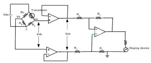
The transducer bridge circuit has resistors and the value of these resistors change according to the changes in the physical conditions. The figure below shows (ref. internet) an Instrumentation Amplifier using Transducer Bridge. Let RT be the transducer bridge and
Fig 9 Instrumentation Amplifier using Transducer Bridge When the bridge is under balanced condition Va = Vb RA(Vdc)/(RA+RT) = RB(Vdc)/(RB+RC) The value of input to the amplifier is VDiff = Vb – Va = 0 The output of the amplifier is zero. When there is a change in the physical quantity being measured, the voltage Va will no longer be equal to Vb. This is because the resistance of the transducer device changes from RT to (RT ± ΔR). The resistances RB and RC are constant and hence the voltage VB remains same as before, i.e. Vb = RB(Vdc)/(RB+RC) Va = RA(Vdc)/(RA+RT+ ΔR) The differential voltage VDiff is, VDiff = Vb – Va VDiff = {RB(Vdc)/(RB+RC)} – {RA(Vdc)/(RA+RT+ ΔR)} For RA = RB = RC = RT = R VDiff = {R(Vdc)/(2R)} – {R(Vdc)/(2R+ ΔR)} VDiff = {RVdc[2R+ΔR] – R.Vdc.2R}/ 2R(2R+ΔR) VDiff = ΔR(Vdc)/{2(2R+ΔR)} Vb>Va when VDiff is positive The output voltage is then given as VO = (R3/R2)Vd Vo = (R3/R2) [ΔR(Vdc)/{2(2R+ΔR)}] As the change in resistance ΔR << 2R, Vo can be written as, Vo = (R3/R2)[ΔR/4R](Vdc) Key takeaways The transducer bridge circuit has resistors and the value of these resistors change according to the changes in the physical conditions. |
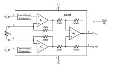
The INA118 low-power instrumentation amplifier is explained below (Ref. Texas Instruments). There is newer version also available now for this device. We will see the datasheet and the pin configuration of the INA118 instrumentation amplifier.
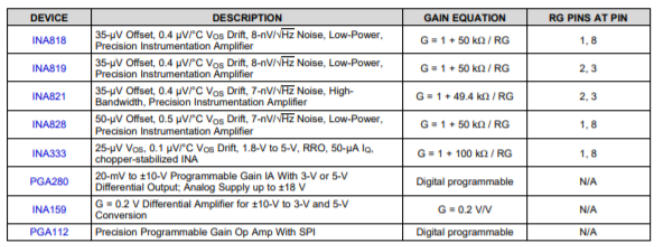
Fig 10 Simplified Diagram It an 8-pin Plastic DIP and SO-8 surface mount package and specified for temperature range of -400C to +850C. The upgraded version is INA818 with lower input offset voltage. The table of comparison of various INA series amplifiers is shown below.
Fig 11 Comparison of Various INA series amplifiers
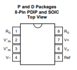
The pin configuration and pin functions is shown below for the better understanding.
Fig 12 Pin configuration
Key takeaways It an 8-pin Plastic DIP and SO-8 surface mount package and specified for temperature range of -400C to +850C.
|
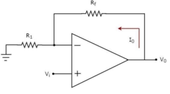
A voltage to current converter or V to I converter, is an electronic circuit that takes current as the input and produces voltage as the output. An op-amp based voltage to current converter produces an output current when a voltage is applied to its non-inverting terminal. The circuit diagram of an op-amp based voltage to current converter is shown in the following figure.
Fig 13 V-I Converter In the circuit shown above, an input voltage Vi is applied at the non-inverting input terminal of the op-amp. According to the virtual short concept, the voltage at the inverting input terminal of an op-amp will be equal to the voltage at its non-inverting input terminal . So, the voltage at the inverting input terminal of the op-amp will be Vi. The nodal equation at the inverting input terminal's node is − ViR1−I0=0 =>I0=VtR1 Thus, the output current I0 of a voltage to current converter is the ratio of its input voltage Vi and resistance R1. We can re-write the above equation as − I0/Vi=1/R1 The above equation represents the ratio of the output current I0 and the input voltage Vi & it is equal to the reciprocal of resistance R1. The ratio of the output current I0 and the input voltage Vi is called as Transconductance.
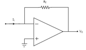
Current to voltage converter A current to voltage converter or I to V converter is an electronic circuit that takes current as the input and produces voltage as the output. An op-amp based current to voltage converter produces an output voltage when current is applied to its inverting terminal. The circuit diagram of an op-amp based current to voltage converter is shown in the following figure.
Fig 14 I-V Converter In the circuit shown above, the non-inverting input terminal of the op-amp is connected to ground. That means zero volts is applied at its non-inverting input terminal. According to the virtual short concept, the voltage at the inverting input terminal of an op-amp will be equal to the voltage at its non-inverting input terminal. So, the voltage at the inverting input terminal of the op-amp will be zero volts. The nodal equation at the inverting terminal's node is − −Ii+0−V0/Rf=0 −Ii=V0/Rf V0=−Rf.Ii Thus, the output voltage, V0 of current to voltage converter is the (negative) product of the feedback resistance, Rf and the input current, It. Observe that the output voltage, V0 is having a negative sign, which indicates that there exists a 1800 phase difference between the input current and output voltage. We can re-write the above equation as − V0/Ii=−Rf The above equation represents the ratio of the output voltage V0 and the input current Ii, and it is equal to the negative of feedback resistance, Rf. The ratio of output voltage V0 and input current Ii is called as Trans-resistance.
Key takeaways A voltage to current converter or V to I converter, is an electronic circuit that takes current as the input and produces voltage as the output. An op-amp based voltage to current converter produces an output current when a voltage is applied to its non-inverting terminal. A current to voltage converter or I to V converter is an electronic circuit that takes current as the input and produces voltage as the output. An op-amp based current to voltage converter produces an output voltage when current is applied to its inverting terminal.
|
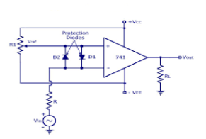
Fig15 Comparator
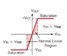
Characteristics of comparator
Fig 16 Voltage levels for comparator
Key takeaway
|
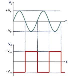
An op-amp detector that has the ability to detect the change from positive to negative or negative to a positive level of a sinusoidal waveform is known as a zero- crossing detector. It is also known to be a square wave generator as the applied input signal is converted into a square wave by the zero -crossing detector.
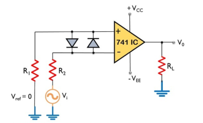
Fig 17 Zero crossing Detector
Here, the input signal Vi is provided to the inverting terminal of the op-amp while the non-inverting terminal is grounded by making use of two resistors R1 and R2. It detects the point where the input signal crosses zero of the reference voltage level. For every crossing, the saturation level of the output signal changes from one to another. The reference level is set at 0 and applied at the non-inverting terminal of the op-amp. The sine wave applied at the inverting terminal of the op-amp is compared with the reference level each time the phase of the wave changes either from positive to negative or negative to positive. Firstly, when positive half of the sinusoidal signal appears at the input. Then the op-amp comparator compares the reference voltage level with the peak level of the applied signal. Vo = Vref – Vi ---------------------------------------(1) And we know the reference level is 0, thus Vo = 0 – ( + Vsat) ----------------------------------------(2) Therefore, Vo = - Vsat ---------------------------------(3) During the negative half of the signal, thus the peak will have a negative polarity. Again
Vo = Vref – Vi ---------------------------------------------(4) Thus, Vo = 0 - ( - Vsat) --------------------------------------------------(5) So, we get Vo = + Vsat ---------------------------------------------(6) In this way, the zero -crossing detector detects the change in the level of the applied signal. Zero crossing detector is also known to be a square wave generator. As the output of the window comparator is nothing but a square wave.
Fig18 Input and output of zero crossing detector V0 for the positive half of the applied signal is – Vsat, This is the reason why we have achieved negative half of the square wave at the output when positive half of the sinusoidal signal is applied. While V0 for the negative half of the sinusoidal signal is + Vsat, Applications:
Key takeaways An op-amp detector that has the ability to detect the change from positive to negative or negative to a positive level of a sinusoidal waveform is known as a zero- crossing detector.
|
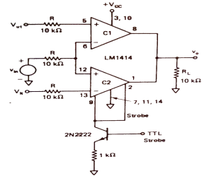
Fig 19 Window Detector using LM1414(Ref 5) The window detectors are used when we need to calculate an unknown value which is not lying between the two precise reference threshold values Vut and Vlt. As we can see from the above figure that voltage Vin is applied to the inverting end of comparator C1 and non-inverting end to C2. TO the + input of C1upper threshold voltage Vut is applied and lower threshold voltage Vlt is applied to the – input of C2. When the value of Vin is in between Vut and Vlt the output is high. The output is low when Vin is above Vut or lower then Vlt. They are usually used in industrial alarms, level detectors and controls, digital computers.
Key takeaway The window detectors are used when we need to calculate an unknown value which is not lying between the two precise reference threshold values Vut and Vlt.
|
The Schmitt Trigger is a logic input type that provides hysteresis or two different threshold voltage levels for rising and falling edge. This is useful because it can avoid the errors when we have noisy input signals from which we want to get square wave signals.
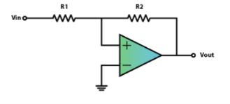
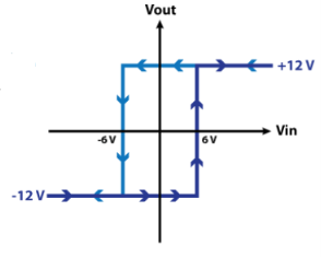
Symmetrical If we add a positive feedback by connecting the output voltage to the non-inverting input with a resistor between them and another resistor between the VIN and the non-inverting input we will get the Schmitt Trigger. Now the output will switch from VCC– to VCC+ when the voltage at the A node will cross 0 volts. That means that now by adjusting the values of the resistors we can set at what value of the VIN input the switch will occur using the following equations. We get these equations with the following relationships. The current “i” through this line equals VIN – VA divided by R1 as well as VA – VOUT divided by R2. So if we replace the VA with zero, as we need that value for the switch to occur, we will get that final equation.
Fig 20 Symmetrical
Va = 0
Fig 21 Symmetrical characteristics
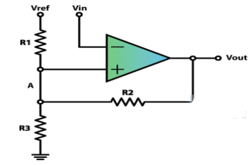
Asymmetrical In order to get two different non-symmetrical thresholds, we can use this circuit of an inverting single powered Schmitt Trigger. Here the VREF voltage is the same as the VCC of the op-amp. Now because the VIN input is connected to the inverting input of the op-amp when its values will reach the upper threshold, the output will switch off to 0 volts, and then when its values will decline to the lower threshold, the output will switch on to 5 volts.
Fig 22 Asymmetrical
Example-1
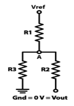
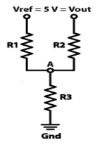
Vout = 0V
Va = 166V Vout = 5V
Va = 333V
Key takeaway The Schmitt Trigger is a logic input type that provides hysteresis or two different threshold voltage levels for rising and falling edge. This is useful because it can avoid the errors when we have noisy input signals from which we want to get square wave signals.
|
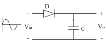
Fig 23 Peak detector In the positive half cycle, diode D is forward biased and capacitor C starts charging. When input reaches its peak value, capacitor gets charged to positive peak value.
But in practice, output is taken across some load RL, so when input voltage decreases capacitor discharges through load RL. To avoid this, select RL of very large value so that capacitor discharges very slowly hence almost hold the charge. Whatever charge it lost through RL is gets back in next half cycle.
Key takeaway The diode D is acting as an instant switch, so supply gets loaded. |
4.14.1 Log Amplifier
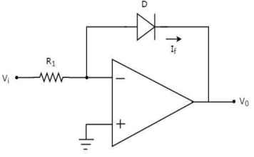
Fig 24 Log Amplifier The equation for input voltage will be
If = The current flowing through diode is given as
Where: Is = Saturation Current Vf = Voltage drop across diode in forward bias VT = Thermal equivalent voltage For feedback loop the KVL equation will be 0-Vf -V0 = 0 Vf = -V0 Substituting Vf in above equation of If
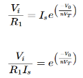
Equating both equations of If
Taking natural log of both sides we get
The above equations shows that the output is natural log of the applied input.
4.14.2 Antilog Amplifier
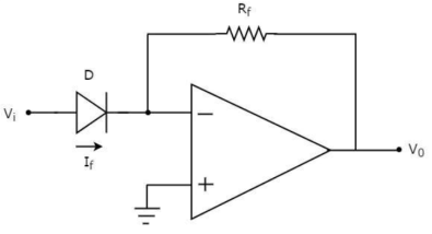
Fig 25 Antilog Amplifier Applying KCL at input terminal we get
The current flowing through diode is given as
Substituting If in above voltage equation we get
At inverting terminal applying KVL we get
Substituting Vf in equation of V0 we get
The above equations shows that the output is natural antilog of the applied input.
Key takeaways For Log Amplifier
For Antilog Amplifier
|
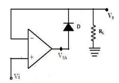
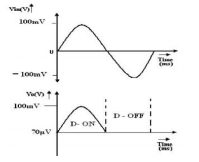
The major limitation of conventional rectifiers is that it cannot rectify AC voltages below forward voltage drop VD (0.7V) of a diode. The precision rectifier will make it possible to rectify input voltage of a very small magnitude even less than forward voltage drop of diode. The diode can be used in AM detector where power is negligible and we want information in the signal. Rectifier circuits used for circuit detection with op-amps are called precision rectifiers.
Fig 26 Precision Rectifier The below figure shows a non-inverting precision rectifier. The diode used is called as precision diode. When the voltage VI is positive the voltage VOA is also positive. When Vi<0the voltage VOA becomes negative and hence reverse biasing the diode and making Vo =0. When the value of input voltage Vi< When the value of input voltage Vi>
Fig 27 Input and Output of Precision Rectifier
Key takeaway The precision diode operates in first quadrant when Vi>0 and V0>0. The precision diode operates in third quadrant when diode is connected in reverse bias.
|
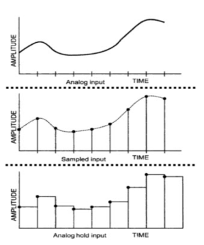
Need for Sample and Hold Circuits If the input analog voltage of an ADC changes more than ±1/2 LSB, then there is a severe chance that the output digital value is an error. For the ADC to produce accurate results, the input analog voltage should be held constant for the duration of the conversion. It is based on a sampling command and holds the output value at its output until the next sampling command is arrived. The following image shows the input and output of a typical Sample and Hold Circuit.
Fig 27 Input and output of S/H circuit
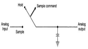
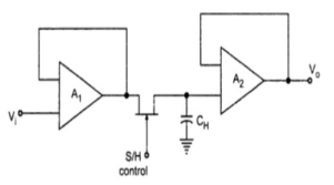
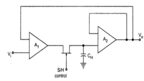
This sample and hold circuit consist of two basic components:
Fig 28 Open loop s/h circuit
Fig 29 Closed loop s/h circuit
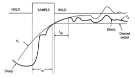
Fig 30 S/H characteristics Acquisition Time (tac) The time required for the charge in the holding capacitor to rise up to a level that is close to the input voltage during the sampling is called acquisition time. It is affected by three factors:
Aperture Time (tap) The time delay between the initiation of VO tracking the Vi and the initiation of the hold command is called the Aperture Time. This delay is usually due to the propagation delays through the driver and the switch circuits. For a precise timing operation, the hold command must be initiated in advance by an amount of aperture time. Aperture Uncertainty (∆ tap) The Aperture time will not be the same for all the sample and will vary from sample to sample. This uncertainty is called Aperture Uncertainty. This will severely affect the advancing of the hold command. Hold Mode Settling Time (ts) The hold mode settling time is the time taken by the output VO to settle within the specified error band (usually 1%, 0.1% or 0.01%) after the application of hold command. Hold Step During the switching from sample mode to hold mode, there might an unwanted transfer of charge between the switch and the holding capacitor (mainly due to the parasitic capacitances). This will affect the capacitor voltage as well as the output voltage. This change in the output voltage from the desired voltage is called Hold Step. Feedthrough Again, the parasitic capacitances in the switch may cause AC coupling between VO and Vi in hold mode. As a result, the output voltage may vary with changes in the input voltage and this is referred to as feedthrough. Droop Voltage Droop is a phenomenon where the voltage across the holding capacitor drops down due to leakage currents. Advantages
Key takeaways: They are used in
|
References:
1. George Clayton and Steve Winder, “Operational Amplifiers”, 5th Edition Newnes.
2. S.Salivahanan & Bhaaskaran, “Linear Integrated Circuits”, 1st Edition, Tata McGraw Hill.
3. T.R Ganesh Babu, “Linear Integrated Circuits”, 3rd Edition, SciTech Publication
4. Sergio Franco, “Design with op-amp &Analog Integrated Circuits”, 3rd Edition, Tata McGraw Hill
5. Ramakant. A. Gayakwad, “Op-Amps & Linear Integrated Circuits”, 3rd Edition, PHI
