Unit-6
Monolithic IC Applications
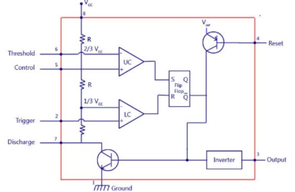
Fig 1 IC 555 Timer
For IC555 timer working as a flip flop or as a multi-vibrator, it has a particular set of configurations. Some of the major features include:
- It operates from a wide range of power ranging from +5 Volts to +18 Volts supply voltage.
- Sinking or sourcing 200 mA of load current.
- The external components should be selected properly so that the timing intervals can be made into several minutes along with the frequencies exceeding several hundred kilohertz.
- The output of a 555 timer can drive a transistor-transistor logic (TTL) due to its high current output.
- It has a temperature stability of 50 parts per million (ppm) per degree Celsius change in temperature which is equivalent to 0.005 %/ °C.
- The duty cycle of the timer is adjustable.
- Also, the maximum power dissipation per package is 600 mW and its trigger and reset inputs has logic compatibility.
Key takeaway
They can be used as frequency divider, PWM, SR F/F, missing pulse detection etc.
The 555 generally operates in 3 modes:
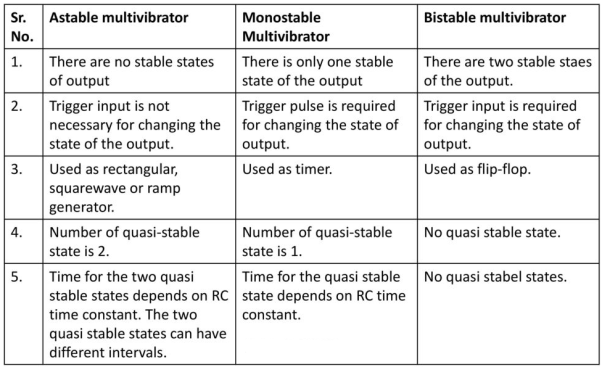
- A-stable
- Mono-stable
- Bi-stable modes.
Astable mode
|
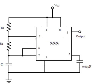
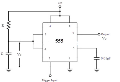
Fig 2 Astable Multivibrator
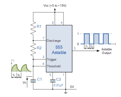
It is self-triggered multivibrator as pin 2 and 6 are connected. The supply is given through pin 8 and the output is obtained through pin 3. The timer will be reset if a low signal is given to pin 4. The capacitor is connected across pin 5 so that the external noise or any dc level are filtered. The resistor pair R1 and R2 form a circuit for determining the width of the output pulse.
|
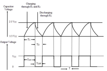
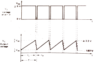
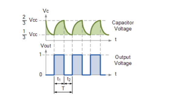
Fig 3 Capacitor and Output voltage waveform
During charging the capacitor charges through R1 and R2 and voltage across capacitor rises exponentially and during discharging the capacitor discharges through R2 and voltage falls exponentially. The output is obtained across pin 3.
The time for which capacitor charges from 1/3VCC to 2/3VCC is equal to the time the output is high which is given by
tc= 0.69(R1+R2) C
The discharging time from 2/3Vcc to 1/3VCC is given as
td= 0.69 R2C
The total period of output waveform is given by
T = tc+ td = 0.69(R1+2R2) C
The frequency of oscillations is given by
f0 =  =
= 
The duty cycle is defined as the ratio of the charging time of capacitor at which the output is high to the total time period.
%duty cycle =  x 100
x 100
Applications of Astable Multivibrator
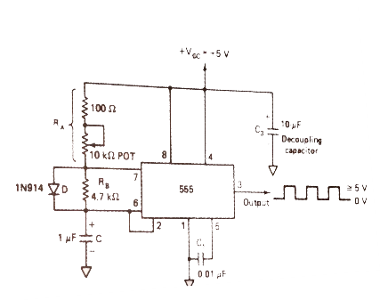
Square wave Oscillator: The astable multivibrator shown in the figure below [Ref.1] can be used to generate square wave oscillations. The diode is connected across RB and the diode and capacitor are charged through RA to a voltage of 2/3 of VCC. The capacitor discharges through RB and Q1. The discharging of capacitor when reaches 1/3VCC the discharging stops.
|
Fig 4 Astable multivibrator as square wave oscillator
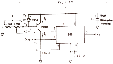
Free-Running Ramp Generator
The circuit diagram is shown below [Ref.1]. The transistor Q1 is turned on by the comparator 1 when voltage across capacitor is 2/3Vcc. The capacitor C discharges through Q1. When capacitor discharges the voltage across C is 1/3Vcc, comparator 2 turns off Q1. The time period is given as
T = VCCC/3IC
Fig 5 Free Running Ramp generator circuit
|
Fig 6 Output waveform
IC = (VCC-VBE)/R
The free running frequency of ramp generator is given by
f0 = 3IC/VCCC
The output waveform is shown in above figure.
Mono-stable mode
If the stable output is set at high (1), the output of the timer is high (1). At the application of an interrupt, the timer output turns low (0). Since the low state is unstable it goes to high (1) automatically after the interrupt passes. The monostable multivibrator using IC555 is shown below.
|
Fig 7 Monostable multivibrator using 555
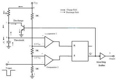
The output is taken through pin 3. The supply is connected to pin 8. A small capacitor is connected to filter noise. The working is shown below in figure and explained as well.
|
Fig 8 555 connected as monostable multivibrator
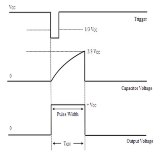
The discharge transistor will go to saturation when the F/F is reset. The discharge of C takes place through drain of CMOS. During negative pulse comparator 2 compares the pulse with reference voltage of 1/3 Vcc and output is low until the input becomes greater than the reference voltage. The output of F/F is set high when the output goes below 1/3Vcc. The output at pin 3 is high.
|
Fig 9 Input and Output waveform
When the C discharges the transistor is off and the voltage decays exponentially. This is input to the comparator 1 with reference voltage 2/3Vcc. The output is still high obtained at pin 3. The output of comparator is high when the threshold voltage becomes more than the reference voltage. Due to this the F/F is reset and output goes to zero. When the output is low the capacitor discharges completely and the transistor goes into saturation.
Pulse width
The voltage across C is Vc = Vcc (1-e-t/RC)
When voltage across capacitor is 2/3Vcc
2/3Vcc = Vcc (1-e-t/RC)
e-t/RC= 1/3
Taking log of both sides and solving we get
t= 1.098RC
The pulse width of rectangular pulse is 1.1RC (approx..)
Application of Monostable Multivibrator
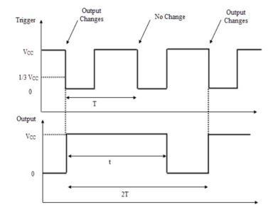
The monostable multivibrator can be used as frequency divider by adjusting the time interval off charging. The charging time is made larger than the period of input pulse the device acts as divide-by-2 network. By proper selection of R and C the timing interval can be controlled. The waveform is shown below.
|
Fig 10 Divide-by-2 circuit waveform
When negative input pulse is applied the output goes high and will remain high irrespective of any other input pulse application as the timing interval s greater than the time period of trigger pulse. The circuit is triggered for every alternate negative going pulse.
Pulse Stretcher
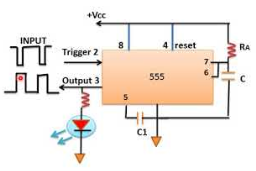
This application makes use of the fact that output pulse width of monostable multivibrator is larger than the negative pulse width of trigger pulse. The output of monostable multivibrator is the stretched form of the input pulse. The pulse stretcher is shown below.
|
Fig 11 Pulse Stretcher
Bi-stable mode
For example, if we have a high (1) output, it will go low(0) once it receives an interrupt and stays low (0) till the next interrupt changes the status.
|
Fig12 Bistable Multivibrator using 555 timer and the output waveform
In the 555 Oscillator circuit above, pin 2 and pin 6 are connected allowing the circuit to re-trigger itself on each and every cycle allowing it to operate as a free running oscillator.
During each cycle capacitor, C charges up through both timing resistors, R1 and R2 but discharges itself only through resistor, R2 as the other side of R2 is connected to the discharge terminal, pin 7.
Then the capacitor charges up to 2/3Vcc which is determined by 0.693(R1+R2)C combination and discharges itself down to 1/3Vcc (the lower comparator limit) determined by the 0.693(R2*C) combination.
This results in an output waveform whose voltage level is approximately equal to Vcc – 1.5V and whose output “ON” and “OFF” time periods are determined by the capacitor and resistors combinations.
The individual times required to complete one charge and discharge cycle of the output is therefore given as:
t 1 = 0.693 (R1 + R2). C and t 2 = 0.693 x R2 x C where, R is in Ω and C in Farads. T = t1 + t2 = 0.693 (R1 + 2 R2) . C f = 1/T = 1.44/ (R1 + 2 R2) . C Duty Cycle = TON / TOFF + TON = R1 + R2 / (R1 + 2R2) %
|
Example-1
t1 – capacitor charge “ON” time is calculated as: t1 = 0.693(R1 + R2). C = 0.693(1000 +2000) x 10 x 10 -6 = 0.021 s= 0.21 msec t2 – capacitor discharge “OFF” time is calculated as: t2 = 0.693 R2. C = 0.693 X 2000 x 10 x 10 -6 = 14ms Total periodic time (T) is therefore calculated as: T = t1 + t2 = 21 ms + 14 ms = 35 ms. The output frequency, ƒ is therefore given as: f = 1/T = 1/35ms = 28.6 Hz Giving a duty cycle value of: Duty Cycle = R1 + R2 / (R1 + 2 R2) = 1000 + 2000/ (1000 + 2 x 2000) = 60%
|
Key takeaways
|
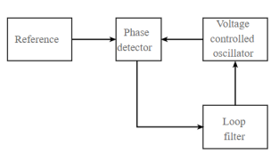
A phase-locked loop consists of a phase detector and a voltage-controlled oscillator. The output of the phase detector is the input of the voltage-controlled oscillator (VCO) and the output of the VCO is connected to one of the inputs of a phase detector which is shown below in the basic block diagram. When these two devices are feed to each other the loop forms.
A basic phase locked loop, PLL, consists of three basic elements:
|
Fig 13 Block Diagram of PLL
- Phase comparator / detector: As the name implies, this circuit block within the PLL compares the phase of two signals and generates a voltage according to the phase difference between the two signals.
- Voltage controlled oscillator, VCO: The voltage-controlled oscillator is the circuit block that generates the radio frequency signal that is normally considered as the output of the loop. Its frequency can be controlled over the operational frequency band required for the loop.
- Loop filter: This filter is used to filter the output from the phase comparator in the phase locked loop, PLL. It is used to remove any components of the signals of which the phase is being compared from the VCO line, i.e. the reference and VCO input. It also governs many of the characteristics of the loop including the loop stability, speed of lock, etc.
Operation
The diagram for a basic phase locked loop shows the three main element of the PLL: phase detector, voltage- controlled oscillator and the loop filter.
In the basic PLL, reference signal and the signal from the voltage- controlled oscillator are connected to the two input ports of the phase detector.
The output from the phase detector is passed to the loop filter and then filtered signal is applied to the voltage- controlled oscillator.
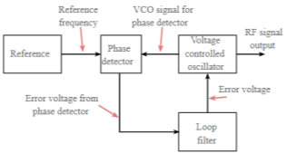
The Voltage Controlled Oscillator, VCO, within the PLL produces a signal which enters the phase detector. The phase of the signals from the VCO and the incoming reference signal are compared and a resulting difference or error voltage is produced. This corresponds to the phase difference between the two signals.
The error signal from the phase detector passes through a low pass filter which governs many of the properties of the loop and removes any high frequency elements on the signal.
Once through the filter the error signal is applied to the control terminal of the VCO as its tuning voltage. The sense of any change in this voltage is such that it tries to reduce the phase difference and hence the frequency between the two signals.
Initially the loop will be out of lock, and the error voltage will pull the frequency of the VCO towards that of the reference, until it cannot reduce the error any further and the loop is locked.
When the PLL, phase locked loop, is in lock a steady state error voltage is produced. By using an amplifier between the phase detector and the VCO, the actual error between the signals can be reduced to very small levels.
However, some voltage must always be present at the control terminal of the VCO as this is what puts onto the correct frequency.
|
Fig 14 PLL showing voltages
The fact that a steady error voltage is present means that the phase difference between the reference signal and the VCO is not changing. As the phase between these two signals is not changing means that the two signals are on exactly the same frequency.
Key takeaways:
The phase locked loop has three main elements: phase detector, voltage- controlled oscillator and the loop filter. When the PLL, phase locked loop, is in lock a steady state error voltage is produced. By using an amplifier between the phase detector and the VCO, the actual error between the signals can be reduced to very small levels.
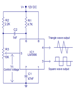
These oscillators are the one whose output frequency can be varied by varying the amplitude of input voltage signal. It is also known as voltage to frequency converter. The block diagram is shown below. The resistor R1 and capacitor C1 determines the frequency of oscillations. Through terminal 5 Vc is applied. As the capacitor charges by current source and linearly discharges through external capacitor triangular wave is generated.
|
Fig 15 VCO using 566
The charge discharge action is provided by Schmitt trigger action. The square wave output is due to the Schmitt trigger. Resistor R1 and capacitor C1 form the timing components. Capacitor C2 is used to prevent the parasitic oscillations during VCO switching. Resistor R3 is used to provide the control voltage Vc. Triangle and square wave outputs are obtained from pins 4 and 3 respectively.
Key takeaways
It is also known as voltage to frequency converter. These oscillators are the one whose output frequency can be varied by varying the amplitude of input voltage signal.
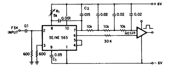
Fig 16 IC 565 PLL
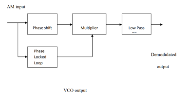
A PLL may be used to demodulate AM signals as shown in the figure below. The PLL is locked to the carrier frequency of the incoming AM signal. The output of VCO which has the same frequency as the carrier, but unmodulated is fed to the multiplier.
Since VCO output is always 900 before being fed to the multiplier. This makes both the signals applied to the multiplier and the difference signals, the demodulated output is obtained after filtering high frequency components by the LPF.
Since the PLL responds only to the carrier frequencies which are very close to the VCO output, a PLL AM detector exhibits high degree of selectivity and noise immunity which is not possible with conventional peak detector type AM modulators.
|
Fig 17 AM Demodulation
FM Demodulation:
If PLL is locked to a FM signal, the VCO tracks the instantaneous frequency of the input signal. The filtered error voltage which controls the VCO and maintains lock with the input signal is the demodulated FM output. The VCO transfer characteristics determine the linearity of the demodulated output.
Since, VCO used in IC PLL is highly linear, it is possible to realize highly linear FM demodulators.
Application
The PLL is widely used in frequency synthesis to generate spectrally pure signals and, if necessary, to operate as an analog or digital frequency or phase modulator.
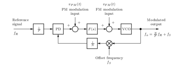
Frequency multiplication or division, frequency addition or subtraction may be performed, using a PLL in conjunction with programmable frequency dividers and mixers as shown in Fig.
As a result, the output frequency fo depends on the reference fR and offset fS frequencies, moreover, on the division ratios of frequency dividers. In frequency synthesis, the PLL input is called reference signal and its frequency is denoted by fR.
To optimize the system performance, frequently a multiloop circuit configuration is used.
|
Fig 18 Frequency Synthesis
In frequency synthesis, the dominant noise sources are the VCO, frequency dividers, mixers, and phase detectors.
The main design goals are to minimize the output phase noise, to avoid the generation of spurious output signals, and to minimize the unwanted output FM caused by the periodic output of the phase detector.
These requirements can be satisfied with special PD configurations, such as sample-and-hold phase detector or phase-frequency detector with a charge-pump circuit.
In addition to frequency synthesis, PLLs may be also used as FM or PM modulators.
The corresponding transfer functions for FM and PM are
sΘo(s) = [1 − H(s)]KvVFM(s)
Θo(s) = H(s) N AK VPM(s) (3)
where Kv and N/(AK) are the gains of the FM and PM modulators, respectively.
H(s) and [1 − H(s)] denote the closed-loop transfer and error functions, respectively.
However, since the frequency synthesizer has a frequency divider in the feedback path, the loop gain becomes
K = KgKdKv
Key takeaway
In addition to frequency synthesis, PLLs may be also used as FM or PM modulators. A PLL may be used to demodulate AM signals.
|
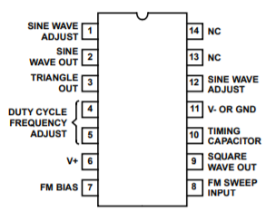
Fig 19 Pin Diagram of IC 8038
|
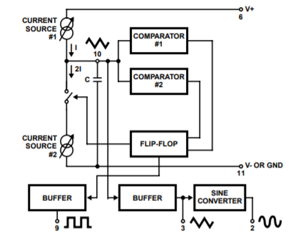
Fig 20 Block diagram of IC 8038
It is a 14 pin PDIP chip. The sine wave is obtained through pin 2. The triangular wave through pin 3. The supply is given through pin 6. An external capacitor C is charged and discharged by two current sources. Current source #2 is switched on and off by a flip-flop, while current source #1 is on continuously. Assuming that the flip-flop is in a state such that current source #2 is off, and the capacitor is charged with a current I, the voltage across the capacitor rises linearly with time.
When this voltage reaches the level of comparator #1 (set at 2/3 of the supply voltage), the flip-flop is triggered, changes states, and releases current source #2. This current source normally carries a current 2I, thus the capacitor is discharged with a net-current I and the voltage across it drops linearly with time. When it has reached the level of comparator #2 (set at 1/3 of the supply voltage), the flip-flop is triggered into its original state and the cycle starts again.
With the current sources set at I and 2I respectively, the charge and discharge times are equal. Thus, a triangle waveform is created across the capacitor and the flip-flop produces a square wave. The sine wave is created by feeding the triangle wave into a nonlinear network. This network provides a decreasing shunt impedance as the potential of the triangle moves toward the two extremes.
Key takeaways:
It is a monolithic IC which can produce various waveforms such as sine, square, triangular, sawtooth, pulse with high accuracy
References:
1. Ramakant. A. Gayakwad, “Op-Amps & Linear Integrated Circuits”, 3rd Edition, PHI
2. S.Salivahanan&Bhaaskaran, “Linear Integrated Circuits”, 1st Edition, Tata McGraw Hill.
3. T.R Ganesh Babu, “Linear Integrated Circuits”, 3rd Edition, SciTech Publication
4. Sergio Franco, “Design with op-amp &Analog Integrated Circuits”, 3rd Edition, Tata McGraw Hill
