The most basic element in the design of large- scale integrated circuit is the transistor. The type of transistor available is the Metal-Oxide-Semiconductor Field Effect Transistor (MOSFET). These transistors form as a sandwich'' consisting of semiconductor layer, a slice or wafer, which from a single crystal of silicon; a layer of silicon dioxide and a layer of metal. These layers are patterned in a manner which permits transistors to be formed in the semiconductor material the substrate'.
The diagram showing a typical MOSFET
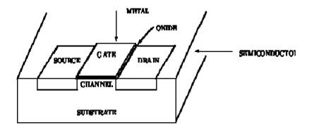
Figure1. MOS Transistor
The transistor consists of three regions, labelled as the source'', gate'' and the drain''. The area labelled as the gate region forms a sandwich consisting of the underlying substrate material. The electrical charge or current can flow from the source to the drain depending on the charge applied to the gate region. The semiconductor material in the source and drain region are doped'' with a different type of material than in the region under the gate, so NPN or PNP type structure exists between the source and drain region of a MOSFET.
In Figure 2 (a), the source and drain regions are doped with N type material and the substrate doped with P type material. Such a transistor is called an N channel MOSFET.
If they were doped with P type material, and the substrate doped with N type material as in Figure 2 (b), the device would be called a P channel MOSFET.
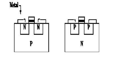
Figure 2(a) N channel MOSFET (b) P channel MOSFET
Key takeaways:
MOS-technology is the dominating LSI-technology. MOS-transistors have been scaled from long to short channels.
An n-channel enhancement type MOSFET with vGS and vDS applied. The normal directions of current flow are indicated.
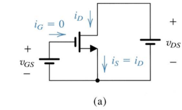
Figure 3. N-channel enhancement type MOSFET
The i-v characteristics comprise a family of curves.
• Each curve corresponds to different value of VGS.
The ID - VDS characteristics for a device with Vt = 1 V and kn(W/L) = 0.5 mA/V2.
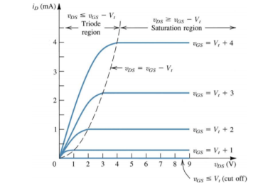
Figure 4. V-I characteristics of NMOS
Three distinct regions of operation can be clearly seen:
Cutoff region:
vGS ≤ Vt no channel induced --------------------------------------(1)
iD = 0-----------------------------------------------------------------------------(2)
Triode region: vGS> Vt channel induced -----------------------------------(3)
vDS ≤ vGS− Vt continuous channel -----------------------------------------------------(4)
iD = k n’ W/ L [(vGS−Vt)vDS– 1/ 2 v2DS -----------------------------------------------(5)
Saturation region:
vGS> Vt channel induced -------------------(6)
vDS≥vGS− Vt pinched − off channel ---------------------(7)
iD = 1/ 2 k n ‘(W/ L) (vGS− Vt) 2-----------------------------------------------(8)
Boundary between triode and saturation regions: vDS = vGS− Vt.
In saturation current is independent of vds and increases as the square of vgs. This is termed as square law behaviour. In saturation MOSFET is an ideal current source. The current does not depend on vds.
PMOS
Figure 5 shows the transfer characteristics of p-type enhancement MOSFETs We see that t IDS remains zero (cutoff state) until VGS becomes equal to -VT, because the channel is formed to connect the drain terminal of the device with its source terminal. After this, however IDS seems to increase in reverse direction with the decrease in the value of VDS. This means that the device is functioning in its ohmic region wherein the current through the device increases with an increase in the applied voltage that is VSD.
However as VDS becomes equal to –VP, the device enters into saturation during which a saturated amount of current (IDSS) flows through the device, by the value of VGS.
Further the value of saturation current flowing through the device increases as the VGS becomes more and more negative i.e. saturation current for VGS3 is greater than that for VGS2 and that in the case of VGS4 is much greater than both of them as VGS3 is more negative than VGS2 while VGS4 is much more negative when compared to either of them (Figure 2b). In addition, from the locus of the pinch-off voltage VGS becomes more and more negative and even the negativity of VP also increases.
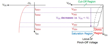
Figure 5. Transfer and Output characteristics
Key Takeaways:
The curves are obtained, keeping the transistor in its saturation region. This means that the current has a parabolic relation with the gate-to-source when it exceeds the threshold voltage.
Consider the schematic diagram of inverter.
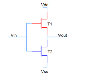
Figure 6. CMOS Inverter
CMOS inverter consists of two transistors a pull-up pMOS transistor(T1) and a pull-down nMOS transistor(T2). When the input voltage Vin is equal to Vdd we get an output voltage of Vss mostly equal to 0 and vice versa. Since it inverts the logic level of input this circuit is called an inverter.
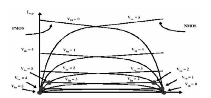
Figure 7.I-V characteristics
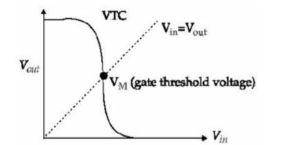
Figure 8.Transfer characteristics
The I-V characteristics of the p-device is reflected about x-axis. This step is followed by taking the absolute values of the p device, Vds and superimposing the two characteristics. Solving Vinn and Vinp and Idsn=Idsp gives the desired transfer characteristics of a CMOS inverter as in fig7.
Key takeaways:
When a high voltage (~ Vdd) is given at input terminal (A) of the inverter, the PMOS becomes an open circuit, and NMOS switched OFF so the output will be pulled down to Vss.
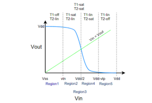
Figure 9. Voltage transfer characteristics
The VTC is divided into five regions(1-5) . The above shown curve is possible when both T1 and T2 are matched for optimum operation. Optimum operation is achieved when Vin = Vdd/2 and we get Vout = Vdd/2 . This is achieved by adjusting width and length of both T1 and T2 as other parameters like mobility, oxide capacitance varies between different technologies.
Consider the following table:
Device | Cutoff | Linear | Saturated |
NMOS | 1. Vgsn<Vtn
| 1. Vgsn>Vtn 2. Vdsn<Vgsn - Vtn | 1. Vgsn>Vtn 2. Vdsn>Vgsn - Vtn |
PMOS | 1. Vgsp>Vtp | 1. Vgsp<Vtp 2. Vdsp>Vgsp - Vtp | 1. Vgsp<Vtp 2. Vdsp<Vgsp - Vtp |
Region-1
In this region the input is in the range of (0,Vtn). Since the input voltage is less than Vtn, the NMOS is in cutoff region. No current flows from Vdd to Vss, The entire Vdd will appear at the Output terminal.
Region-2
In this region the input is in the range of (Vtn,Vdd/2). Since the input voltage is greater than Vtn the NMOS is conducting and it jumps to saturation as it has large Vds across it(Vout is high). PMOS still remains in the linear region.
Region-3
In this region the input voltage is Vdd/2. At this point the output voltage is also Vdd/2 as in figure-2. At this voltage both the NMOS and PMOS are in saturation and the output drops drastically from Vdd to Vdd/2. At this point a large amount of current flows from the supply. Most of the power consumed in CMOS inverter is at this point. Care should be taken that the Input should not stay at Vdd/2 for more amount of time.
Region-4
In this region the input voltage is in the range of (Vdd/2 ,Vdd-Vtp). Here the PMOS remains in saturation as Vout< Vin - Vtp and Vgsp<Vtp. But the NMOS moves from saturation to linear region since the drain to source voltage now is less than Vgsn-Vtn.
Region-5
In this region the input voltage is in the range of (Vdd-Vtp,Vdd). Here the PMOS moves from saturation to cutoff as the Vgsp is so high that Vgsp>Vtp. The NMOS still remains in linear as the drain to source voltage now is less than Vgsn-Vtn.
Key takeaways:
A CMOS inverter contains PMOS and a NMOS transistor connected at the drain and gate terminals, a supply voltage VDD at the PMOS source terminal, and a ground connected at the NMOS source terminal, were VIN is connected to the gate terminals and VOUT is connected to the drain terminals.
Assume that the goal is to size the NOR gate such that it has approximately the same delay as an inverter with the following device sizes: NMOS 0.5mm/0.25mm and PMOS 1.5mm/0.25mm. Since the pull-down path in the worst case is a single device, the NMOS devices (M1 and M2 ) can have the same device widths as the NMOS device in the inverter.
For output to be high, both devices must be turned on. Because the resistances add, the devices must be made two times larger compared to the PMOS in the inverter (i.e., M3 and M4 must have a size of 3mm/0.25mm). Since PMOS devices have a lower mobility relative to NMOS devices, stacking devices in series must be avoided as much as possible.
A NAND implementation is clearly preferred over a NOR implementation for implementing generic logic.
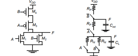
Figure 10. Sizing of a NOR gate to produce the same delay as an inverter with size of NMOS:
Key takeaways:
N- and P- networks must implement complementary functions Duality sufficient for correct operation.
The two elements may be two-component pins, two traces, a pad and a trace, a pad, and a pin, or any other two conductive elements on the board. As the intrinsic capacitor plates have a charge differential there is an opportunity for current flow. Now, current does not flow through the capacitor instead an electrical charge differential is accumulated between the plates. As this charge differential increases, a corresponding decrease in electron flow is available for the desired signal path that negatively impacts signal integrity.
Effects Of Parasitic Capacitance
Key takeaways:
Parasitic capacitance, or stray capacitance is an unavoidable and usually unwanted capacitance that exists between the parts of an electronic component or circuit simply because of their proximity to each other.
References:
1. Fundamentals of Modern VLSI DevicesBook by Tak H. Ning and Yuan Taur
2. Introduction to VLSI systemsBook by Carver Mead
3. VLSI physical design automationTextbook by Sadiq Sait
4. Cmos Digital Integrated CircuitsBook by Sung-Mo Kang and Yusuf Leblebici
