Unit 3
SEMICONDUCTOR PHYSICS
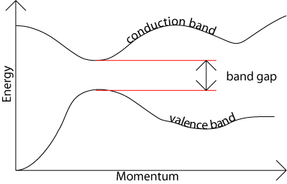
The band gap represents the minimum energy difference between the top of the valence band and the bottom of the conduction band; However, the top of the valence band and the bottom of the conduction band are not generally at the same value of the electron momentum. In a direct band gap semiconductor, the top of the valence band and the bottom of the conduction band occur at the same value of momentum, as in the schematic below.
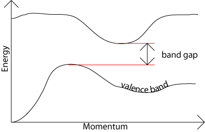
In an indirect band gap semiconductor, the maximum energy of the valence band occurs at a different value of momentum to the minimum in the conduction band energy:
The difference between the two is most important in optical devices. As has been mentioned in the section charge carriers in semiconductors, a photon can provide the energy to produce an electron-hole pair.
Each photon of energy E has momentum p = E / c, where c is the velocity of light. An optical photon has an energy of the order of 10–19 J, and, since c = 3 × 10⁸ ms–1, a typical photon has a very small amount of momentum.
A photon of energy Eg, where Eg is the band gap energy, can produce an electron-hole pair in a direct band gap semiconductor quite easily, because the electron does not need to be given very much momentum. However, an electron must also undergo a significant change in its momentum for a photon of energy Eg to produce an electron-hole pair in an indirect band gap semiconductor. This is possible, but it requires such an electron to interact not only with the photon to gain energy, but also with a lattice vibration called a phonon in order to either gain or lose momentum.
The same principle applies to recombination of electrons and holes to produce photons. The recombination process is much more efficient for a direct band gap semiconductor than for an indirect band gap semiconductor, where the process must be mediated by a phonon.
The highest energy level that an electron can occupy at the absolute zero temperature is known as the Fermi Level. The Fermi level lies between the valence band and conduction band because at absolute zero temperature the electrons are all in the lowest energy state.
In a p type semiconductor, there is an increase in the Density of unfilled States. Thus, more electrons can be accommodated at lower energy states. In a n type semiconductor, the DOS is increased. Thus, electrons have to be accommodated at higher energy levels.
Fermi level is also defined as the work done to add an electron to the system. More positive (more holes) in a p type semiconductor, mean lesser work needs to be done. Hence a lower Fermi level.
When the material is at a temperature higher than OK, it receives thermal energy from surroundings i.e. electrons are thermally excited. As a result, they move into the higher energy levels which are unoccupied at OK. The occupation obeys a statistical distribution called Fermi – Dirac distribution law.
According to this distribution law, the probability F(E) that a given energy state E is occupied at a temperature T is given by

Here F(E) is called Fermi – Dirac probability function. It indicates that the fraction of all energy state (E) occupied under thermal equilibrium ‘K’ is Boltzmann constant.
Fermi Dirac distribution function:
Mathematically the probability of finding an electron in the energy state E at the temperature T is expressed as
Where, is the Boltzmann constant
T is the absolute temperature
Ef is the Fermi level or the Fermi energy
Now, let us try to understand the meaning of Fermi level. In order to accomplish this, put
in equation (1). By doing so, we get,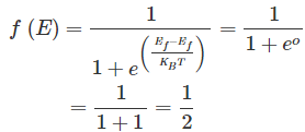
This means the Fermi level is the level at which one can expect the electron to be present exactly 50% of the time.
Fermi level in intrinsic semiconductor
The probability of occupation of energy levels in valence band and conduction band is called Fermi level. At absolute zero temperature intrinsic semiconductor acts as perfect insulator. However as the temperature increases free electrons and holes gets generated.
In intrinsic or pure semiconductor, the number of holes in valence band is equal to the number of electrons in the conduction band. Hence, the probability of occupation of energy levels in conduction band and valence band are equal. Therefore, the Fermi level for the intrinsic semiconductor lies in the middle of forbidden band.
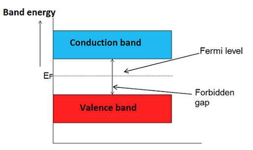
Fermi level in the middle of forbidden band indicates equal concentration of free electrons and holes.
The hole-concentration in the valence band is given as

The electron-concentration in the conduction band is given as

Where KB is the Boltzmann constant
T is the absolute temperature of the intrinsic semiconductor
Nc is the effective density of states in the conduction band.
Nv is the effective density of states in the valence band.
The number of electrons in the conduction band is depends on effective density of states in the conduction band and the distance of Fermi level from the conduction band.
The number of holes in the valence band is depends on effective density of states in the valence band and the distance of Fermi level from the valence band.
For an intrinsic semiconductor, the electron-carrier concentration is equal to the hole-carrier concentration.
It can be written as
p = n = ni
Where P = hole-carrier concentration
n = electron-carrier concentration
And ni = intrinsic carrier concentration
The fermi level for intrinsic semiconductor is given as,

Where EF is the fermi level
EC is the conduction band
EV is the valence band
Therefore, the Fermi level in an intrinsic semiconductor lies in the middle of the forbidden gap
Fermi level in extrinsic semiconductor
In extrinsic semiconductor, the number of electrons in the conduction band and the number of holes in the valence band are not equal. Hence, the probability of occupation of energy levels in conduction band and valence band are not equal. Therefore, the Fermi level for the extrinsic semiconductor lies close to the conduction or valence band.
Fermi level in n-type semiconductor
In n-type semiconductor pentavalent impurity is added. Each pentavalent impurity donates a free electron. The addition of pentavalent impurity creates large number of free electrons in the conduction band.
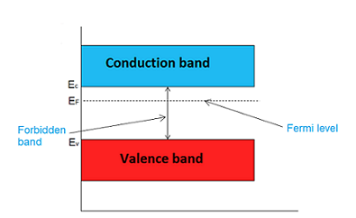
At room temperature, the number of electrons in the conduction band is greater than the number of holes in the valence band. Hence, the probability of occupation of energy levels by the electrons in the conduction band is greater than the probability of occupation of energy levels by the holes in the valence band. This probability of occupation of energy levels is represented in terms of Fermi level. Therefore, the Fermi level in the n-type semiconductor lies close to the conduction band.
The Fermi level for n-type semiconductor is given as

Where EF is the fermi level.
EC is the conduction band.
KB is the Boltzmann constant.
T is the absolute temperature.
NC is the effective density of states in the conduction band.
ND is the concentration of donar atoms.
Fermi level in p-type semiconductor
In p-type semiconductor trivalent impurity is added. Each trivalent impurity creates a hole in the valence band and ready to accept an electron. The addition of trivalent impurity creates large number of holes in the valence band.
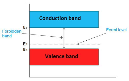
At room temperature, the number of holes in the valence band is greater than the number of electrons in the conduction band. Hence, the probability of occupation of energy levels by the holes in the valence band is greater than the probability of occupation of energy levels by the electrons in the conduction band. This probability of occupation of energy levels is represented in terms of Fermi level. Therefore, the Fermi level in the p-type semiconductor lies close to the valence band.
The Fermi level for p-type semiconductor is given as

Where NV is the effective density of states in the valence band.
NA is the concentration of acceptor atoms.
1. EFFECTS OF IMPURITIES ON CONDUCTION:
A common method for generating even more charge carriers in a semiconductor is by doping. That is, replacing a few atoms of the base material with atoms of a different element.
These impurities will contribute an excess electron or hole which is loosely bound and hence can be excited into the conduction band by thermal energy.
For example, doped junction silicon crystal with adjoining P-type substances (aluminum, gallium) and N-type substances (phosphorus, arsenide) is used to form a diode.
The key thing about these semiconductor materials is that we can very carefully and precisely introduce impurities and this leads to the development of extraordinarily useful devices for electronic applications.
This process is known as "DOPING"
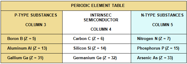
MAJORITY AND MINORITY CHARACTERS:
The doping process introduces extremely precise concentrations of elements:
- From Column 3 of the periodic table: P–Extrinsic elements (P or Positive),
- From Column 5 of the periodic table: N–Extrinsic elements (N or Negative).
P-Extrinsic semiconductor:
In P-type doping, boron (B) or gallium (Ga) is the dopant. Boron and gallium each have only three outer electrons.
When mixed into the silicon lattice, they form “holes” in the lattice where a silicon electron has nothing to bond to. The absence of an electron creates the effect of a positive charge, hence the name P-type.
Holes can conduct current. A hole happily accepts an electron from a neighbour, moving the hole over a space.
Example - boron p-type:
Typical of these is boron from column 3 and arsenic from Column 5.
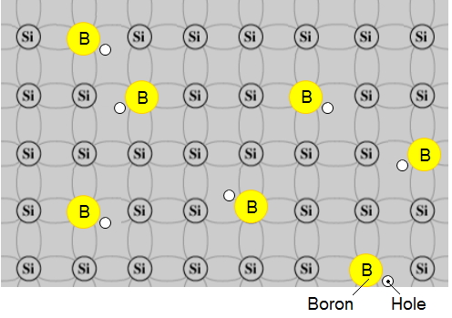
Use the 2-D representation of pure Silicon with each atom sharing electrons with 4 adjacent atoms as shown next figure:
We show an atom of boron which has just three electrons in its outer most shell before it enters the silicon arrangement.
The next sketch depicts the doped material:
It is easy to see that the newly embedded boron atom introduces an available "hole" into the silicon structure but the whole material is electrically stable, particularly at absolute zero of temperature.
N-Extrinsic semiconductor:
In N-type doping, phosphorus (P) or arsenic (As) is added to the silicon in small quantities.
Phosphorus and arsenide each have five outer electrons, so they're out of place when they get into the silicon lattice.
The fifth electron has nothing to bond to, so it's free to move around. It takes only a very small quantity of the impurity to create enough free electrons to allow an electric current to flow through the silicon.
N-type silicon is a good semiconductor.
Electrons have a negative charge, hence the name N-type.
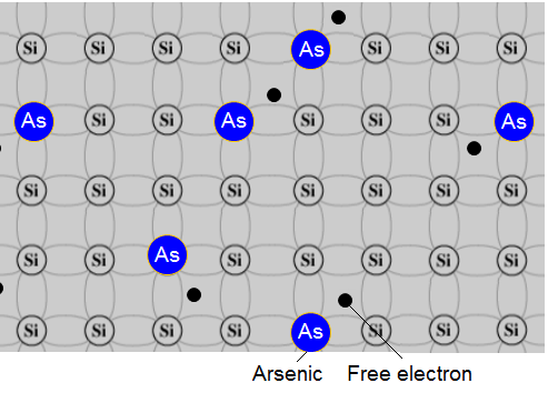
Example - arsenic n-type:
The sequence of doping with arsenic shows the atom of arsenic which has 5 electrons in its outermost shell before it enters the pure silicon. Four of them are used to covalent links and the fifth is a free electron.
When we are trying to determine the position of the Fermi level we assume the semiconductor is in equilibrium. EF on the band diagram is a function of temperature and carrier concentration. This can be seen from the equations used to determine the position of the Fermi level.
Intrinsic semiconductor |  |
n-type semiconductor |  |
p-type semiconductor |  |
If the temperature is varied, the Fermi level will also vary.
Concentration of impurity on fermi level
A donor is an element with typically one more valence electron than the element that forms the semiconductor. An acceptor is an element with typically one fewer valence electron than the element that forms the semiconductor. An ion is an electrically charged atom or group of atoms. Ionization occurs when an electron is removed from or added to an atom, in this case it would be the dopant atoms.
The donor's extra electron is weakly bound and needs very little energy, thermal or otherwise, to break the bond and become a free electron. As temperature is increased, more and more of these bonds are broken, until all the donors are ionized, producing an increase in electron concentration. At room temperature, we assume all the donors are ionized.
At 0 K the electrons at the donor sites do not receive enough energy to make it to the conduction band, so the ratio between the majority carrier concentration and the doping concentration n/ND = 0. As the temperature is increased , more donor electrons make it to the conduction band, but at temperatures below 150 K all the donor sites have not been ionized so the ratio n/ND < 1 and the majority carrier concentration is made up of the donor electrons that have made it to the conduction band. At room temperature, we assume all the donors are ionized, meaning all donor electrons are in the conduction band, so the ratio n/ND = 1 and the majority carrier concentration is made up of the donor electrons. At very high temperatures, above 500 K, electrons from the valence band receive enough energy to make it to the conduction band and outnumber the electrons from the donor sites, so the ratio n/ND > 1 and the majority carrier concentration is now made up of electrons from the valence band in the conduction band, as in an intrinsic semiconductor.
Acceptors have one fewer valence electron than the neighboring semiconductor atoms and will readily accept an electron in order to completely bond. Very little energy is needed for an electron to travel to one of the acceptor sites and be trapped. As the temperature is increased, more electrons become trapped in acceptor sites, until all the acceptors are ionized, causing the hole concentration to increase. At room temperature, we assume all the acceptors are ionized.
It can be applied toward acceptors by substituting p/NA in place of n/ND. At 0 K the electrons in the valence band do not receive enough energy to jump to an acceptor site and create a hole, so the ratio p/NA = 0. At temperatures below 150 K the ratio p/NA < 1 because all the acceptor sites have not been ionized, so the majority carrier concentration is made up of the holes left behind by trapped electrons in the acceptor sites. At room temperature we assume all the acceptors have been ionized. The ratio p/NA = 1 because the majority carrier is made up of the holes created by the ionized acceptors. At very high temperatures, above 500 K, the ratio p/NA > 1 because the holes created by electrons from the valence band jumping to the conduction band outnumber the holes that had been created by acceptors, so the majority carrier concentration is made up of holes created by valence electrons in the conduction band, as in an intrinsic semiconductor
Dopants in an intrinsic semiconductor perform two major functions
1. They increase carrier concentration of a particular polarity (i.e. electrons or holes) so that the overall conductivity is higher. Usually this is orders of magnitude higher than the intrinsic semiconductor and is dominated by either electrons or holes i.e. the majority carriers.
2. Dopants also stabilize carrier concentration around room temperature. For Si, the saturation regime extends from roughly 60 K to 560 K.
Consider the general conductivity equation

For extrinsic semiconductors with either n or p much higher than the minority carrier concentration equation 1 can be written as

µe and µh are the drift mobilities of the carriers. They are given by

The drift mobilities are a function of temperature and in extrinsic semiconductors they depend on the dopant concentration.
This dependence comes from the scattering time, τe and τh, which is the time between two scattering events.
Another way of writing the scattering time is in terms of a scattering cross section (S). This is given by;

Where vth is the mean speed of the electrons (thermal velocity) and Ns is the number of scatters per unit volume.
When an electric field E is applied across a semiconductor material, the charge
Carriers attain a drift velocity vd.
So, drift velocity
Vd=µE----------------(1)
The relation between current density J and drift velocity vdis
J=Nqvd
Where N is the carrier concentration
q is the charge of electron or hole
From equations (1) and (2), we get

_ is the mobility of charge carrier.
The above equation shows the general expression for drift current density.
Drift current density due to electrons is

Where is the electrons carrier concentration and
µe the mobility of electrons
Drift current density due to holes is

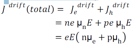
Total drift current density:
Let be the excess electron concentration. Then according to Fick’s law, the rate of
Diffusion of charge carriers is proportional to concentration gradient is

Hence
Rate of diffusion of charge:
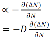
Where D is the diffusion coefficient of charge carriers
The negative sign indicates decrease of N with increase of x
So, the diffusion current density Jdiffuis:

The expression for total current density due to holes is

The expression for total current density due to electrons is

When a material carrying current is subjected to a magnetic field in a direction perpendicular to direction of current, an electric field is developed across the material in a direction perpendicular to both the direction of magnetic field and current direction. This phenomenon is called “Hall-effect”.
Explanation:
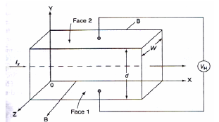
* Consider a semi-conductor, and current passes along the X-axis and a magnetic field Bz is applied along the Z-direction, a field Ey is called the Hall field which is developed in the Y-direction.
*In P-type semi-conductor, holes move with the velocity “V” in the “+”ve X-direction. As they move across the semiconductor the holes experience a transverse force ‘Bev’ due to the magnetic field.
* This force drives the holes down to the lower face. As a result, the lower face becomes +vely charged and –ve charge on the upper surface creating the hall field in the Y-direction. The Hall field exerts an upward force on holes equal to Ee.
* In the steady sate, two forces just balance and as a result, no further increase of + ve charge occurs on Face1.
* In N type semiconductor, the majority charge carriers are electrons experiences a force in the downward direction and lower face gets – vely charged. As a result, Hall field will be in the Y – direction.
Hall Coefficient:
Hall field𝐸𝐻, for a given material depends on the current density J and the applied magnetic field B.
i.e. 𝐸𝐻α JB
𝐸𝐻= 𝑅𝐻α JB
Since,
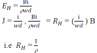
This is called hall coefficient.
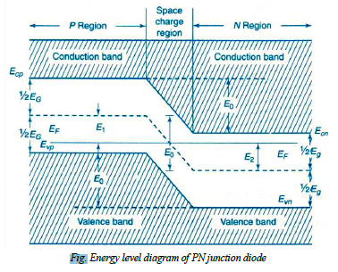
The contact potential VB across the junction is due to the potentials of depletion region on n- side denoted by vn and p – side denoted by vp
i.e.: VB = Vn - Vp→(7)
The energy levels of valance band, conduction band and Fermi level of both p- type and n- type semiconductors. When Pn junction is formed the Fermi, levels become common for both the types formation of potential barrier is represented in fig.
The contact potential separates the energy bands in p—type and n- type crystals. Since there is no net current flow at equilibrium i.e. under unbiased condition, it should have common Fermi level. Hence in PN junction diode the valance and conduction band energy levels Evp and Ecp of p- type and at higher level compared to the valance and conduction band energy levels Evn and Ecn of n-type. The electric field EB across the junction is given by
EB = Evp - Evn = Ecp - Ecn = e VB →(8)
Biased PN Junction:
When the PN junction is unbiased, it is in equilibrium and contact potential VB (= Vn- Vp) appears across the depletion region.
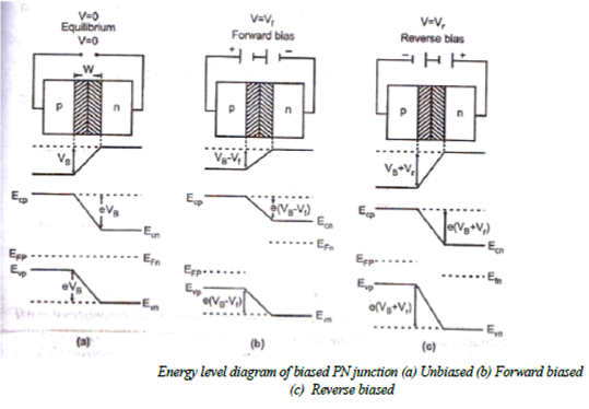
*If now an external voltage is applied across depletion region such that positive of the source is connected to the p-type side and negative of the source is connected to the n-type then junction is said to be “Forward biased”. This voltage Vf appears across the depletion region. As the contact potential difference VB acts from n to p the electrostatic potential barrier is lowered and is given by VB -Vf.
* If the external voltage Vr is applied across the depletion region such that the negative of the source is connected to the p- type side and positive of source is connected to the n- type side then the junction is said to be “Reverse biased:. Since this potential act along VB, the electrostatic potential barrier increases. And is given by VB+Vr. Thus on application of forward bias, the electric field in the transition region reduces and the application of reverse bias increases the electric field in the transition region.
* Since the width of the transition region is propositional to the square root of the electrostatic potential barrier, the width of the transition region decreases under forward bias and increases under reverse bias.
LED:
Light Emitting Diodes (LEDs) are the most widely used semiconductordiodes among all the different types of semiconductor diodes available today. Light emitting diodes emit either visiblelight or invisible infraredlight when forward biased. The LEDs which emit invisible infrared light are used for remote controls
When Light Emitting Diode (LED) is forward biased, freeelectrons in the conduction band recombines with the holes in the valence band and releases energy in the form of light.
The process of emitting light in response to the strong electricfield or flow of electric current is called electroluminescence.
A normal p-n junctiondiode allows electric current only in one direction. It allows electric current when forward biased and does not allow electric current when reverse biased. Thus, normal p-n junction diode operates only in forward bias condition.
Light Emitting Diode (LED) works only in forward bias condition. When Light Emitting Diode (LED) is forward biased, the free electrons from n-side and the holes from p-side are pushed towards the junction.
When free electrons reach the junction or depletion region, some of the free electrons recombine with the holes in the positive ions. We know that positive ions have less number of electrons than protons. Therefore, they are ready to accept electrons. Thus, free electrons recombine with holes in the depletion region. In the similar way, holes from p-side recombine with electrons in the depletion region.
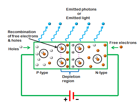
Because of the recombination of free electrons and holes in the depletion region, the width of depletion region decreases. As a result, more charge carriers will cross the p-n junction.
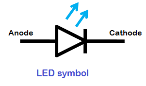
The symbol of LED is similar to the normal p-n junction diode except that it contains arrows pointing away from the diode indicating that light is being emitted by the diode.
Zener diode:
A Zener diode is a silicon semiconductor device that permits current to flow in either a forward or reverse direction. The diode consists of a special, heavily doped p-n junction, designed to conduct in the reverse direction when a certain specified voltage is reached.
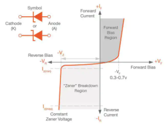
The Zener diode has a well-defined reverse-breakdown voltage, at which it starts conducting current, and continues operating continuously in the reverse-bias mode without getting damaged. Additionally, the voltage drop across the diode remains constant over a wide range of voltages, a feature that makes Zener diodes suitable for use in voltage regulation.
The Zener diode operates just like the normal diode when in the forward-bias mode, and has a turn-on voltage of between 0.3 and 0.7 V. However, when connected in the reverse mode, which is usual in most of its applications, a small leakage current may flow. As the reverse voltage increases to the predetermined breakdown voltage (Vz), a current starts flowing through the diode. The current increases to a maximum, which is determined by the series resistor, after which it stabilizes and remains constant over a wide range of applied voltage.
Zener breakdown
The breakdown is either due to the Zener breakdown effect that occurs below 5.5 V, or impact ionization that occurs above 5.5 V. Both mechanisms result in the same behavior and do not require different circuitry; however, each mechanism has a different temperature coefficient.
The Zener effect has a negative temperature coefficient while the impact effect experiences a positive coefficient. The two temperature effects are almost equal at 5.5 V and cancel out each other to make the Zener diodes rated at around 5.5 V the most stable over a wide range of temperature conditions.
Photovoltaic cell:
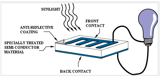
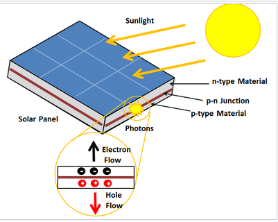
a solar panel works by allowing photons, or particles of light, to knock electrons free from atoms, generating a flow of electricity. Solar panels actually comprise many, smaller units called photovoltaic cells. (Photovoltaic simply means they convert sunlight into electricity.) Many cells linked together make up a solar panel
Photovoltaic cells, through the photovoltaic effect, absorb sunlight and generate flowing electricity. This process varies depending on the type of solar technology, but there are a few steps common across all solar photovoltaic cells.
Step 1: Light is absorbed by the PV cell and knocks electrons loose
First, light strikes a photovoltaic cell and is absorbed by the semiconducting material it is made from (usually silicon). This incoming light energy causes electrons in the silicon to be knocked loose, which will eventually become the solar electricity you can use in your home.
Step 2: Electrons begin to flow, creating an electrical current
There are two layers of silicon used in photovoltaic cells, and each one is specially treated, or “doped”, to create an electric field, meaning one side has a net positive charge and one has a net negative charge. This electric field causes loose electrons to flow in one direction through the solar cell, generating an electrical current.
Step 3: The electrical current is captured and combined with other solar cells
Once an electrical current is generated by loose electrons, metal plates on the sides of each solar cell collect those electrons and transfer them to wires. At this point, electrons can flow as electricity through the wiring to a solar inverter and then throughout your home.
