Unit 6
ENGINEERING MATERIALS AND APPLICATIONS
Substance that blends the structures and properties of the normally disparate liquid and crystalline solid states. Liquids can flow, for example, while solids cannot, and crystalline solids possess special symmetry properties that liquids lack. Ordinary solids melt into ordinary liquids as the temperature increases—e.g., ice melts into liquid water. Some solids actually melt twice or more as temperature rises. Between the crystalline solid at low temperatures and the ordinary liquid state at high temperatures lies an intermediate state, the liquid crystal. Liquid crystals share with liquids the ability to flow but also display symmetries inherited from crystalline solids. The resulting combination of liquid and solid properties allows important applications of liquid crystals in the displays of such devices as wristwatches, calculators, portable computers, and flat-screen televisions
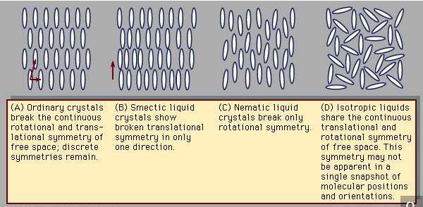
6.1.1 Nematic, Semitic and cholesteric phases
Randomly positioned in parallel, nematic LCs react quickly to electric fields, which is why they are used in the great majority of LCD screens. Meaning "thread" in Greek, nematic LCs are monostable and return to their original alignment when the electric field is removed.
The simplest liquid crystal phase is called the nematic phase (N).
It is characterized by a high degree of long range orientational order but no translational order. Molecules in a nematic phase spontaneously order with their (for calamitic molecules) long axes roughly parallel. A schematic diagram of a nematic phase. An uniformly aligned nematic has a preferred direction, often described in terms of a unit vector called the director,  . More generally a bulk nematic will contain domains. The orientation of the director is constant in each domain but is different in different domains. Viewed under a polarizing microscope the defect regions linking these domains appear as dark threads.
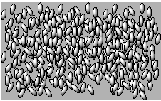
Smectic phases
It have further degrees of order compared to the nematic phase. In the simplest smectic phase, the smectic-A (SmA) phase, the molecules order into layers, with the layer normal parallel to the director. Within the layers, liquid like structure remains
Closely related to the SmA phase is the smectic-C (SmC) phase. Here the molecules form a layer structure but the long axes of the molecules, and hence the director, lies at an angle to the layer normal There are many other smectic phases which have long range order within the layers. Smectic phases can also be formed by chiral molecules, leading to chiral smectic phases.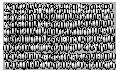
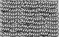
Cholesteric liquid crystals (CLCs)
This is a fascinating genre from the liquid crystalline material family, due, in large part, to the unique optical properties its mesoscopic helical structure imparts. When suitably aligned and when the helical length scale is below 1 micron, the material exhibits structural colouration in the UV–VIS–NIR spectral regions, which has been utilised in numerous applications ranging from the technologically sophisticated including a variety of display motifs to the simplistic like mood rings. Control of the ‘colour’, due to reflection from the unique anisotropic media, has been a long-standing research topic within the community. Since liquid crystal LC materials are inherently a fluid with low viscosity, the ability to change the colour in response to a suitable stimulus such as temperature, e-field and light, has been the focus of numerous research efforts. The fundamental physical properties and the associated applications of low molar mass, thermotropic LCs. The author is a long-standing contributor to the LC community with many contributions during the particular busy time period of investigation several decades ago.
6.1.2 Liquid crystal display:
Stands for "Liquid Crystal Display." LCD is a flat panel display technology commonly used in TVs and computer monitors. It is also used in screens for mobile devices, such as laptops, tablets, and smartphones.
LCD displays don't just look different than bulky CRT monitors, the way they operate is significantly different as well. Instead of firing electrons at a glass screen, an LCD has backlight that provides light to individual pixels arranged in a rectangular grid. Each pixel has a red, green, and blue RGB sub-pixel that can be turned on or off. When all of a pixel's sub-pixels are turned off, it appears black. When all the sub-pixels are turned on 100%, it appears white. By adjusting the individual levels of red, green, and blue light, millions of color combinations are possible.
Each LCD screen contains a matrix of pixels that display the image on the screen. Early LCDs had passive-matrix screens, which controlled individual pixels by sending a charge to their row and column. Since a limited number of electrical charges could be sent each second, passive-matrix screens were known for appearing blurry when images moved quickly on the screen. Modern LCDs typically use active-matrix technology, which contain thin film transistors, or TFTs. These transistors include capacitors that enable individual pixels to "actively" retain their charge. Therefore, active-matrix LCDs are more efficient and appear more responsive than passive-matrix displays
An LCD's backlight may either be a traditional bulb or LED light. An "LED display" is simply an LCD screen with an LED backlight. This is different than an OLED display, which lights up individual LEDs for each pixel. While the liquid crystals block most of an LCD's backlight when they are off, some of the light may still shine through (which might be noticeable in a dark room). Therefore, OLEDs typically have darker black levels than LCDs.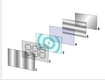
The terminology ‘multiferroics’ refers to those materials where more than one ferroic order, i.e. (anti)ferromagnetism, ferroelectricity, ferro elasticity, and ferrotoroidicity, coexist in one phase. A combination of these multiple ferroic orders may allow intimate coupling among them, paving the way to realizing cross-control of various ordered parameters. The most striking of such controls is switching magnetization and/or ferroelectric polarization by electric and magnetic fields. Nowadays, the term ‘multiferroics’ is often used specifically for those materials hosting ferroelectric and magnetic behaviours.
Materials that are both ferroelectric and magnetic–multiferroics–are rare. This is because in most ferroelectrics, such as BaTiO3, the ferroelectricity is driven by a hybridization of empty d orbitals with occupied p orbitals of the octahedrally coordinated oxygen ions. This mechanism requires empty d orbitals and thus cannot lead to multiferroic behaviour. There are consequently very few ferroelectrics that exhibit long range magnetic order, and rarer still are materials where these two disparate order parameters exist and exhibit significant coupling. Multiferroics have been of particular interest recently both to understand the fundamental aspects of the novel mechanism that gives rise to this magnetic-ferroelectric coupling, as well as because of the intriguing possibility of using these coupled order parameters in novel device applications. In particular, recent "proof of principle" work has shown that it is possible to control the magnetic phase with an applied electric field, and control the electric polarization with an applied magnetic field.
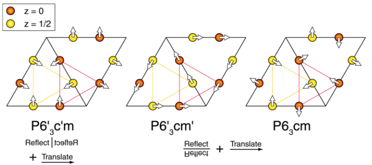
The hexagonal HoMnO3 system of particular interest here is a prototype multiferroic. The holmium-oxygen displacements give rise to a ferroelectric moment along the crystallographic c axis at very high temperatures (TC = 875 K), while the Mn moments order at 72 K. The order parameters are naturally coupled through the Ho-Mn exchange and anisotropy interactions. The crystal structure is shown in the figure, where we see that the Mn spin system has the added interest that the moments occupy a fully frustrated triangular lattice.
6.2.1 Type I & Type II multiferroics and applications
There are two types of multiferroics:
Type-I and type-II
Type-II multiferroics, where ferroelectricity is generated in specific magnetic ordering, are sometimes called magnetism-driven multiferroics. All other single-phase multiferroics that do not have a magnetic origin of ferroelectricity can be categorized as type-I multiferroics. To more precisely capture the intrinsic physics, the type-I or type-II families can be further sub-classified according to the detailed microscopic mechanisms for ferroelectricity. This is rather meaningful, especially for type-I multiferroics. The double-layered magnetic perovskites exhibiting hybrid improper ferroelectricity represent an additionally developed sub-class of type-I multiferroics, which have shown highly designable multiferroicity in recent years
TYPE-I MULTIFERROICS
First of all, BiFeO3 is an unavoidable material if one discusses type-I multiferroics where ferroelectricity and magnetism are believed to originate from two different cations; i.e. the 6s lone pair electrons of Bi give rise to ferroelectricity and the 3d-electrons of Fe lead to canted G-type antiferromagnetic (AFM) order. This represents a major strategy that was initially utilized to ‘produce’ type-I multiferroics, and a variety of Bi-based and Pd-based type-I systems have been synthesized and characterized. An extension of this strategy in concomitance with research progress is exemplified by EuTiO3 where the 4f magnetic moment of Eu and d0-ferroelectricity of Ti coexist, and are efficiently coupled under some specific conditions
TYPE-II MULTIFERROICS
For type-II multiferroic materials, electric polarization is believed to be generated by a specific magnetic order, allowing a remarkable ME response. It was initially discovered in orthorhombic RMnO3and RMn2O5 , and subsequently dozens of materials have been found to show type-II multiferroicity. Three microscopic mechanisms, i.e. the inverse Dzyaloshinskii–Moriya (DM) interaction, exchange stiction, and spin-dependent p–d hybridization, have been proposed. In particular, for materials hosting spiral spin order (SSO), the electric polarization can be sharply and completely flipped from one direction to another, resulting in remarkable ME response, although the inverse DM interaction-induced polarization is generally small (<0.01 μC/cm2) . In contrast, the exchange-striction-induced electric polarization, most likely observed in materials with collinear spin order, can be much larger (>0.1 μC/cm2), and even comparable with conventional ferroelectrics. Recently, a giant polarization of P ∼ 2 μC/cm2 in RMnO3 under pressure, due to exchange striction, was demonstrated. It should be mentioned that the ME coupling in multiferroics dominated by the exchange striction mechanism is usually not as striking as that in multiferroics of spiral spin order, and polarization switching usually requires a relatively high magnetic field. It is noticed that the spin-dependent p–d hybridization mechanism is found only in several materials although a unique ME coupling mode that the electric polarization can be successively rotated by magnetic field has been observed.
Application
In multiferroic thin films, the coupled magnetic and ferroelectric order parameters can be exploited for developing magnetoelectronic devices. These include novel spintronic devices such as tunnel magnetoresistance (TMR) sensors and spin valves with electric field tunable functions. A typical TMR device consists of two layers of ferromagnetic materials separated by a thin tunnel barrier (~2 nm) made of a multiferroic thin film.[44] In such a device, spin transport across the barrier can be electrically tuned. In another configuration, a multiferroic layer can be used as the exchange bias pinning layer. If the antiferromagnetic spin orientations in the multiferroic pinning layer can be electrically tuned, then magnetoresistance of the device can be controlled by the applied electric field One can also explore multiple state memory elements, where data are stored both in the electric and the magnetic polarizations.
Radio and high-frequency devices
Multiferroic composite structures in bulk form are explored for high-sensitivity ac magnetic field sensors and electrically tunable microwave devices such as filters, oscillators and phase shifters (in which the ferri-, ferro- or antiferro-magnetic resonance is tuned electrically instead of magnetically)
Multiferroics have been used to address fundamental questions in cosmology and particle physics. In the first, the fact that an individual electron is an ideal multiferroic, with any electric dipole moment required by symmetry to adopt the same axis as its magnetic dipole moment, has been exploited to search for the electric dipole moment of the electron. Using the designed multiferroic material (Eu, Ba) TiO3, the change in net magnetic moment on switching of the ferroelectric polarisation in an applied electric field was monitored, allowing an upper bound on the possible value of the electron electric dipole moment to be extracted. This quantity is important because it reflects the amount of time-reversal (and hence CP) symmetry breaking in the universe, which imposes severe constraints on theories of elementary particle physics. In a second example, the unusual improper geometric ferroelectric phase transition in the hexagonal manganites has been shown to have symmetry characteristics in common with proposed early universe phase transitions.
A number of other unexpected applications have been identified in the last few years, mostly in multiferroic bismuth ferrite, that do not seem to be directly related to the coupled magnetism and ferroelectricity. These include a photovoltaic effect photocatalysis, and gas sensing behaviour It is likely that the combination of ferroelectric polarisation, with the small band gap composed partially of transition-metal d states are responsible for these favourable properties.
The magnetic properties of the lanthanum manganese oxide class of materials have attracted tremendous interest recently because of the dramatic increase in conductivity these systems exhibit when the magnetic moments order ferromagnetically, either by lowering the temperature or applying a magnetic field. This huge increase in the carrier mobility, which has been given the name "Colossal MagnetoResistivity" (CMR), is both of scientific and technological interest. In particular, it is anticipated that the "half-metallic" behaviour these materials exhibit could provide fully spin polarized electrons for use in “spintronics” applications, for sensors in a variety of applications such as in the automotive industry, and may also provide the next generation of read/write heads for the magnetic data storage industry.
6.3.1 Magnetoresistance, GMR and CMR materials
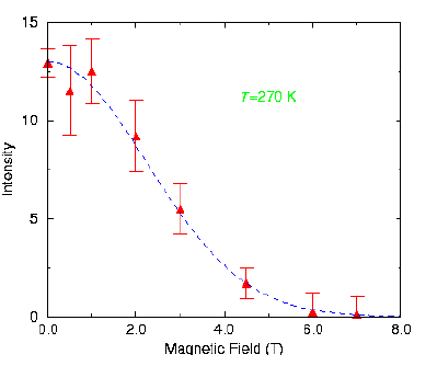
The CMR originates from a magnetically driven insulator-metal transition, where the magnetic, electronic, and structural degrees of freedom are intimately intertwined. Neutron scattering measurements have been used to discover that the transition from the low temperature ferromagnetic-metallic state to the paramagnetic-insulator state is caused by the formation of combined structural/magnetic polarons, which have a size of about one nanometer. The formation of these nanoscale polarons truncates the ferromagnetic phase, and thus explains the first-order nature of the transition. These polarons form a well-defined thermodynamic glass phase above the ferromagnetic ordering temperature, which then melts into a polaron fluid at higher temperatures.
There is a strong similarity between these nanoscale polarons observed in the CMR materials, the polar nanoregions that cause the dramatic piezoelectric response of relaxer ferroelectrics, and the formation of stripes in the high temperature superconducting cuprates. Recent progress in our understanding of these intrinsic nanoscale structures has enabled a deeper understanding of the fundamental properties and shared concepts of all these perovskite-based materials.
The giant magnetoresistance (GMR)--
This effect is a very basic phenomenon that occurs in magnetic materials ranging from nanoparticles over multi-layered thin films to permanent magnets. In this contribution, we first focus on the links between effect characteristic and underlying microstructure. Thereafter, we discuss design criteria for GMR-sensor applications covering automotive, biosensors as well as nanoparticular sensors.
The giant magnetoresistance effect is the change of electric conductivity in a system of metallic layers when an external magnetic field changes the magnetization of the ferromagnetic layers relative to each other. A parallel alignment, like it is depicted in Figure 1a, has usually a lower resistance than an antiparallel alignment, Figure 1b. The effect size is defined as:
ΔR/R=(R↑↓−R↑↑)/R↑↑
Where R↑↑ and R↑↓ are the resistivity’s for parallel and antiparallel alignment, respectively. Alternatively, the ratio is sometimes defined with R↑↓ as denominator. The effect originates from spin-dependent transport of electrons in magnetic metals.
Nowadays the underlying physics of GMR and the interlayer exchange coupling are broadly understood. Nevertheless, when it comes to detail, discrepancies between experimental observations and theoretical models can arise: a realistic theoretical description of electron scattering at lattice discontinuities, disorder or defects is still a crucial factor.
In this review, we intend to provide an overview of different aspects of the GMR effect. The first section will focus on some of the ideas used to describe GMR effects theoretically in multilayers and to extend them into granular systems. Thereafter, we will have a look at different systems in which GMR can occur, with emphasis on the application-relevant side
Spintronics is "Spin based electronics". The idea is to use the electron's spin, as well as it's charge. Electrons can spin in two directions (Spin-Up, Spin-Down, which is actually clockwise and anti-clockwise), and the spin is detectable as weak magnetic energy. Hopefully Spintronics will allow us to do more "work" than electronics, with less effort.
There are many possible usages of Spintronics. One of the obvious ones is memory. MRAM is based on Spintronics, and it promises to be a fast, small and non-volatile memory.
In the future we might see Spintronics based transistors, which will allow us to replace electronics circuit boards with Spintronics ones.
For starters, Spintronic device do not need an electric current to retain their "spin". That means, for example, that MRAM is a non-volatile memory, like FLASH. Spin is more "reliable", and such devices will operate better in high temperature or radiation environments. Theoretically Spintronic devices will be smaller, faster and more powerful than electronic ones
Spin-Valves, which are used in Hard-Disks and sensors today, use Spintronics. Also MRAM, which is based on Spintronics, is advancing nicely, and Ever Spin (formerly part of Freescale) have started selling 4-Mbit MRAM modules. There are several Spintronics-based sensors which are also available today.
As Spintronics uses the spin of electrons, the new field of Valleytronics uses the valley degree of freedom in certain semiconductors - such as graphene or other materials.