Unit - 3
Data Processing Circuits
3.1.1 The Multiplexer
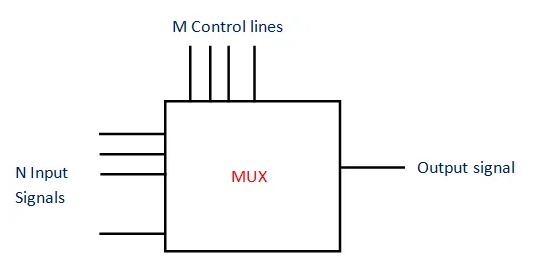
A multiplexer is a combinational logic circuit that connects one or more input lines to a single output line.
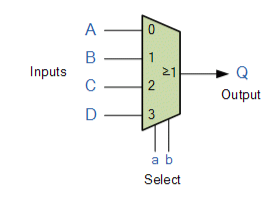
The action of delivering one or more analogue or digital signals over a common transmission line at different times or speeds is referred to as multiplexing, and the equipment we use to do so is referred to as a multiplexer.
The multiplexer, abbreviated as "MUX" or "MPX," is a combinational logic circuit that uses a control signal to switch one of numerous input lines to a single common output line. Multiplexers work like highly rapid acting multiple position rotary switches, connecting or regulating several input lines, referred known as "channels," to the output one at a time.
Multiplexers, often known as MUXs, are digital circuits that employ high-speed logic gates to switch digital or binary data, or analogue circuits that employ transistors, MOSFETs, or relays to switch one of the voltage or current inputs to a single output.
A one-way rotary switch, as pictured, is the simplest basic sort of multiplexer device.
Basic Multiplexing Switch
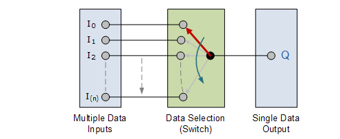
A rotary switch, often known as a wafer switch since each layer of the switch is termed a wafer, is a mechanical device that selects input by rotating a shaft. To put it another way, a rotary switch is a manual switch that may be used to select particular data or signal lines by simply turning the inputs "ON" or "OFF." So, how can we use a digital gadget to select each data input automatically?
Multiplexers, often known as data selectors in digital electronics because they can "select" each input line, are made up of separate Analogue Switches housed in a single IC package, as opposed to "mechanical" selectors like regular switches and relays.
When a single data line or data bus is required to convey two or more separate digital signals, they are utilised as one means of minimising the number of logic gates necessary in a circuit design. A single 8-channel multiplexer, for example.
In most multiplexers, an extra set of inputs called control lines controls the selection of each input line, and the appropriate data input is connected directly to the output based on the binary status of these control inputs, either "HIGH" or "LOW." A multiplexer typically contains an even number of 2n data input lines and a number of “control” inputs equal to the number of data inputs.
Multiplexers are not the same as encoders in terms of how they work. Encoders can convert an n-bit input pattern to numerous output lines that indicate the active input's binary coded (BCD) output equivalent.
As demonstrated, we may construct a simple 2-line to 1-line (2-to-1) multiplexer using basic logic NAND gates.
2-input Multiplexer Design
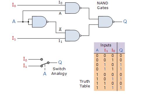
This simple 2-1 line multiplexer circuit, made up of ordinary NAND gates, has an input A that controls which input ( I0 or I1) is sent to the output at Q.
When the data select input, A, is LOW at logic 0, input I1 transfers its data through the NAND gate multiplexer circuit to the output, while input I0 is blocked, as shown in the truth table above. When data choose A is HIGH at logic 1, the situation is reversed, and input I0 now delivers data to output Q while input I1 is blocked.
So, by applying a logic "0" or "1" at A, we may select the proper input, I0 or I1, with the circuit behaving similarly to a single pole double throw (SPDT) switch.
We can only switch 21 inputs since we only have one control line (A), therefore in this simple example, the 2-input multiplexer connects one of two 1-bit sources to a shared output, resulting in a 2-to-1-line multiplexer. The following Boolean expression demonstrates this.
Q = A.I0.I1 + A.I0.I1 + A.I0.I1 + A.I0.I1 + A.I0.I1 + A.I0.I1 + A.I0.I1 + A.I0.I1 + A.I0.I1
This can also be simplified for our 2-input multiplexer circuit:
A.I1 + A.I0 = Q
Utilizing the same technique, we may expand the number of data inputs that can be selected even further, and larger multiplexer circuits can be built using smaller 2-to-1 multiplexers as their basic building blocks. As four inputs equals 22 data control lines, we'd need two data select lines for a four-input multiplexer, resulting in a circuit having four inputs, I0, I1, I2, I3, and two data select lines A and B, as shown.
4-to-1 Channel Multiplexer
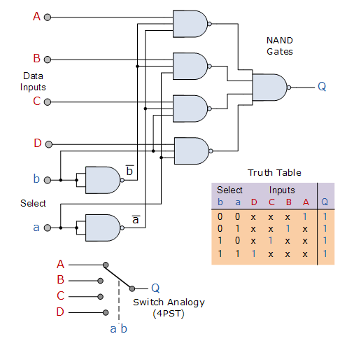
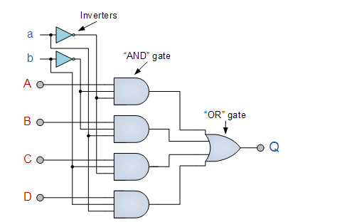
With inputs A through D and data select lines a, b, the Boolean expression for this 4-to-1 Multiplexer is Q = abA + abB + abC + abD.
Just ONE of the four analogue switches is closed at any given time in this example, connecting only one of the input lines A to D to the single output at Q. The addressing input code on lines "a" and "b" determines which switch is closed.
To choose input B to the output at Q in this example, the binary input address would need to be "a" = logic "1" and "b" = logic "0." As a result, we may plot the data selection through the multiplexer as a function of the data choose bits.
Selection of Multiplexer Input Lines

By adding more control address lines (n), the multiplexer will be able to manage more inputs because it can switch 2n inputs, but each control line configuration will only connect ONE input to the output.
Then, in order to implement the Boolean expression above using individual logic gates, seven separate gates consisting of AND, OR, and NOT gates would be required, as illustrated.
4 Channel Multiplexer using Logic Gates
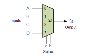
A multiplexer is represented by the following symbol in logic diagrams:
Symbol for a Multiplexer
Multiplexers can do more than merely combine a number of various input lines or channels into a single output. There are also varieties that may switch their inputs to numerous outputs, such as 4-to-2, 8-to-3, or even 16-to-4, and an example of a simple Dual channel 4 input multiplexer (4-to-2) is shown below:
4-to-2 Channel Multiplexer
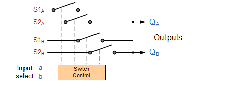
The four input channels are switched to two separate output lines in this example, although larger setups are also feasible. This straightforward 4-to-2 setup could be used to swap audio signals for stereo pre-amplifiers or mixers, for example.
Adjustable Amplifier Gain
Multi-channel multiplexers can be used in digital audio applications as mixers or to adjust the gain of an analogue amplifier digitally, in addition to transferring parallel data in a serial format through a single transmission line or link.
Digitally Adjustable Amplifier Gain
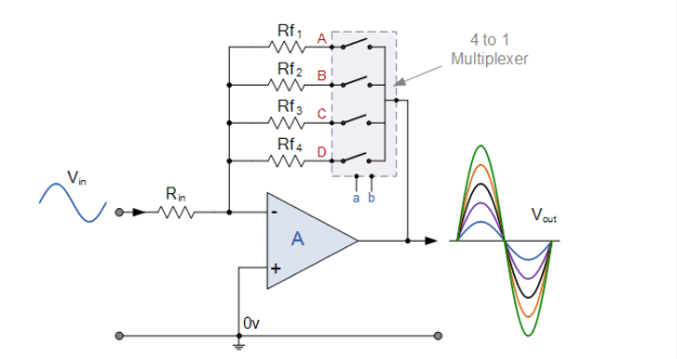
As discovered in the Op-amp tutorials, the voltage gain of the inverting operational amplifier is defined by the ratio between the input resistor, RIN, and its feedback resistor, R.
To pick any feedback resistor to modify the value of R, a single 4-channel (Quad) SPST switch configured as a 4-to-1 channel multiplexer is connected in series with the resistors. The overall voltage gain of the amplifier is determined by the combination of these resistors (Av). The amplifier's voltage gain can then be digitally modified by simply selecting the proper resistor combination.
Because they pick the data to be transferred to the output line, digital multiplexers are also known as "Data Selectors." They are extensively employed in communications and high-speed network switching circuits such as LANs and Ethernet applications.
A single inverting buffer (NOT Gate) is linked to the output of several multiplexer ICs, resulting in a positive logic output (logic "1," HIGH) on one terminal and a complementary negative logic output (logic "0," LOW) on another.
Simple multiplexer circuits can be built using conventional AND and OR gates, as we've seen, but most multiplexers/data selectors come in conventional i.c. Packages, such as the TTL 74LS151 8-input to 1 line multiplexer or the TTL 74LS153 Dual 4-input to 1 line multiplexer. By cascading together two or more smaller devices, multiplexer circuits with a considerably higher number of inputs can be created.
3.1.3 Multiplexers: How Do They Work? (Circuit of 2 to 1, 4 to 1, 8 to 1 MUX)
What Does a Multiplexer Do?
In digital systems, selecting a single data line from numerous data input lines is common, and the data from the selected data input line should be available on the output line. A multiplexer is the digital circuit that performs this function.
A multiplexer is a digital circuit that selects one of the n data inputs and outputs it. The select inputs are used to choose one of the n inputs. We need m choose lines such that 2m=n to choose one of numerous inputs.
One of the n data inputs is picked and transferred to the single output based on the digital code applied at the select inputs. As a result, a multiplexer can have up to 2n data input lines, one select line, and one output line.
The graphic below depicts the block diagram of an n-to-1 multiplexer and its equivalent circuit.
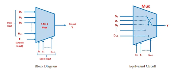
How Does a Multiplexer Work?
The multiplexer functions as a switch with numerous inputs and a single output. At any given time, the output is connected to only one of the n data inputs. As a result, the multiplexer is a digital analogue of an analogue selector switch that combines many functions into one.
Multiplexer Circuit
Multiplexers come in a variety of configurations, including 2-to-1, 4-to-1, and 8-to-1. Each has its own circuit, truth table, boolean expression, and operating principle. Let's take a look at each form of multiplexer separately.
2 to 1 Multiplexer
2 to 1 Multiplexer Circuit
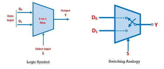
A digital multiplexer circuit with two data inputs D0 and D1, one select line S, and one output Y is known as a 2-to-1 multiplexer. Two AND gates, an OR gate, and a NOT gate are required to build a 2-to-1 multiplexer circuit.
The picture below depicts the block diagram, logic symbol, and switching circuit analogies of a 2-to-1 multiplexer.
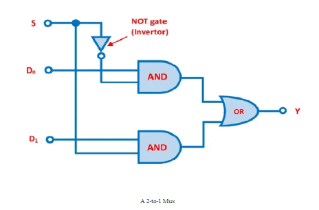
Fig. 2-to-1 Mux
D0 is an applied input to one AND gate, whereas D1 is an applied input to the other AND gate, as illustrated. A select input S is applied as a second input to the second AND gate, and an inverted input S is applied as a second input to the first AND gate. Both the AND gates' outputs are used as inputs to the OR gate. Circuit for a 2 to 1 Multiplexer
2 to 1 Multiplexer Working Principle
When S=0, it is used as a direct input to the second AND gate, and when S=1, it is used as a second input to the first AND gate. We now know that if any one of the AND gate's inputs is zero, the output is also zero. As a result, the second AND gate's output is zero. The output of the first AND gate is identical to its first input, which is Y = D0, because the second input is 1.
When S=1, the exact opposite occurs. The second AND gate output is identical to the first AND gate input in this case, Y = D1, and the first AND gate output is 0.
We may select the proper input, D0 or D1, by supplying a logic ‘0' or ‘1' to the select input S, making the circuit operate as a single pole double throw (SPDT) switch.
2 to 1 Multiplexer Truth Table
The below table shows the truth table for the 2-to-1 multiplexer.
Select input S | Data Input D0 | Data Input D1 | Output Y |
0 | 0 | 0 | 0 |
0 | 0 | 1 | 0 |
0 | 1 | 0 | 1 |
0 | 1 | 1 | 1 |
1 | 0 | 0 | 0 |
1 | 0 | 1 | 1 |
1 | 1 | 0 | 0 |
1 | 1 | 1 | 1 |
Truth Table of 2-to-1 Multiplexer
The 2-input multiplexer creates a 2-to-1 multiplexer by connecting one of two 1-bit sources to a shared output.
2 to 1 Multiplexer Boolean Expression
The boolean expression for the output of the 2-to-1 multiplexer can be written using the truth table.
In simple notation
S | Y |
0 | D0 |
1 | D1 |
As indicated in the table above, when selecting input S=0, the output is Y=D0, and when selecting input S=1, the output is Y=D1. Larger multiplexer circuits can be created using smaller 2-to-1 multiplexers if the number of data inputs can be increased further.
The NAND gate can also be used to implement all of the multiplexers. It's worth noting that NAND and NOR gates are universal gates that can be used to create any digital circuit.
4 to 1 Multiplexer
4 to 1 Multiplexer Circuit Diagram
A digital multiplexer with four data inputs, two select lines, and one output is known as a 4-to-1 multiplexer. We'll need four AND gates, an OR gate, and two NOT gates to make a 4-to-1 multiplexer circuit.
Four inputs, D0, D1, D2, and D3, and two data select lines, S0 and S1, as 4-inputs, indicate = = data control lines in a 4-to-1 multiplexer. Based on the combination of the inputs at the selection lines, one of these four inputs will be connected to the output.
The picture below depicts the block diagram, logic symbol, and switching circuit analogies of a 4-to-1 multiplexer.
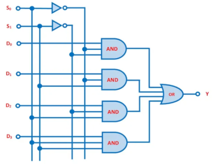
Fig: A 4-to-1 Mux Logic Circuit

4 to 1 Multiplexer Working Principle
The topmost AND gate is enabled and all subsequent AND gates are disabled if both select inputs are enabled. As a result, the data input is chosen and transferred as an output. As a result, we receive the result.
If both select inputs are enabled, just the bottom-most AND gate is active, while all other AND gates are deactivated. As a result, the data input is chosen and transferred as an output. As a result, we obtain output.
4 to 1 Multiplexer Truth Table
The below table shows the truth table for the 4-to-1 multiplexer.
S0 | S1 | Y |
0 | 0 | D0 |
0 | 1 | D1 |
1 | 0 | D2 |
1 | 1 | D3 |
Truth Table of 4-to-1 Multiplexer
The 4-input multiplexer creates a 4-to-1 multiplexer by connecting one of four 1-bit sources to a common output.
4 to 1 Multiplexer Boolean Expression
From the truth table, we can write the Boolean expression for the output.

8 to 1 Multiplexer
8 to 1 Multiplexer Circuit Diagram
A digital multiplexer with 8 data inputs, 3 select lines, and one output is known as an 8-to-1 multiplexer. We'll need 8 AND gates, one OR gate, and three NOT gates to make an 8-to-1 multiplexer circuit.
In 8-to-1 multiplexer, eight inputs D0, D1, D2, D3, D4, D5, D6, and D7, three data select lines that are S0, S1, and S2 as 8-inputs represent 2m = 23 data select lines. Three selection lines regulate the selection of a particular input line in an 8-to-1 multiplexer.
The graphic below depicts the block diagram of an 8-to-1 multiplexer.
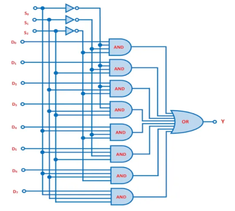
Fig. A 8-to-1 Mux
8 to 1 Multiplexer Working Principle
The topmost AND gate is enabled and all other AND gates are disabled if all three select inputs are S0 = 0, S1 = 0, S3 = 0. As a result, the data input D0 is chosen and sent as an output. As a result, we receive the result Y = D0.
The bottom-most AND gate is enabled and all other AND gates are disabled if all three select inputs are S0 = 1, S1 = 1, S3 = 1. As a result, the data input D7 is chosen and sent as an output. As a result, we have output Y = D7.
8 to 1 Multiplexer Truth Table
The below table shows the truth table for the 8-to-1 multiplexer.
S0 | S1 | S2 | Y |
0 | 0 | 0 | D0 |
0 | 0 | 1 | D1 |
0 | 1 | 0 | D2 |
0 | 1 | 1 | D3 |
1 | 0 | 0 | D4 |
1 | 0 | 1 | D5 |
1 | 1 | 0 | D6 |
1 | 1 | 1 | D7 |
Truth Table of 8-to-1 Multiplexer
3.1.5 Arduino Multiplexer
Multiplexing is a very efficient technique for controlling many components wired together in the form of an array or matrix – and this holds true for Arduino. LEDs, sensors, buttons, and other components found in the best Arduino starting kits are examples of such components.
The diagram below shows how to connect the Multiplexer IC to the Arduino. We used the 74HC4051 multiplexer IC, which has eight channels.
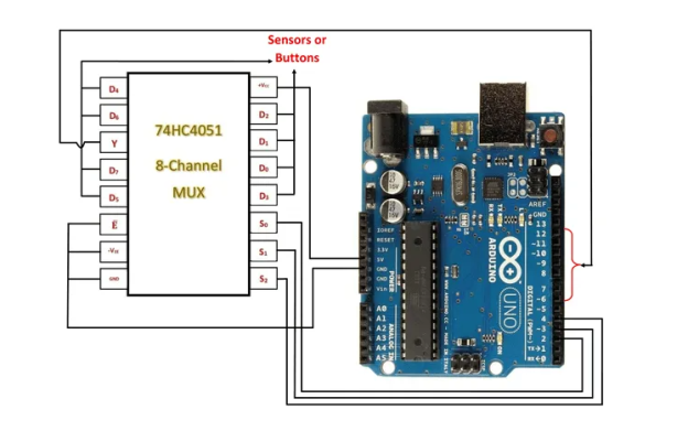
Multiplexer IC 74HC4051 to Arduino Configuration: The IC is powered by +VCC and is connected to the Arduino's 5V supply pin.
The enable pin is connected to the GND pin of Arduino, whereas -VEE is the negative supply voltage pin.
The output is controlled by the control pins S0, S1, and S3, which are connected to the Arduino 2, 3, and 4 pins.
If the chip's inputs are digital, the output Y is linked to any of Arduino's digital input pins 6 to 12. However, if the chip's inputs are analogue, the output pin is connected to Arduino's analogue input pins A0 through A5.
Sensors, buttons, and potentiometers can all be used as multiplexer inputs. It's worth noting that the input to the multiplexers can be analogue or digital. Instead of Arduinos, some individuals prefer to use Raspberry Pis. If you're not sure, check out the Arduino vs Raspberry Pi comparison.
Integrated Circuits with Multiplexers (ICs)
The table below lists the multiplexers integrated circuits (ICs) that are available, as well as their functions and output state.
IC number | Function | Output State |
74150 | 16:1 multiplexer | Inverted output |
74151 | 8:1 multiplexer | Inverted output |
74153 | Dual 4-to-1 multiplexer | Output is equal to input |
74352 | Dual 4-to-1 multiplexer | Inverted output |
74157 | Quad 2-to-1 multiplexer | Output is equal to input |
74158 | Quad 2-to-1 multiplexer | Inverted output |
What is a Multiplexer Tree or Chaining Multiplexers?
Multiplexers with a larger number of inputs can be generated by cascading two or more multiplexers with fewer inputs.
In other words, larger multiplexers can be made by chaining smaller multiplexers together. A multiplexer tree or a chaining multiplexer is what this is called.
Two 4-to-1 and one 2-to-1 multiplexers, for example, can be cascaded to create an 8-to-1 multiplexer. The output of the two 4-to-1 multiplexers is fed into the 2-to-1 multiplexer, and the select lines on the 4-to-1 multiplexers are connected in parallel, resulting in a total of three select inputs, comparable to an 8-to-1 multiplexer. Let's have a look at an example.
Example: Using two 4-to-1 multiplexers, create an 8-to-1 multiplexer.
Solution:
- The 8-to-1 multiplexer is created by cascading two 4-to-1 multiplexers, as shown in the diagram below.
- There are eight data inputs, numbered D0 through D7.
- Both 4-to-1 multiplexers' select inputs S0 and S1 are connected in parallel, while the third select input S2 is utilised to enable one multiplexer at a time.
- Choose your input. S2 is connected directly to MUX-1's Enable(E) terminal, while S2– is attached to MUX-2's enable terminal.
- To achieve the final output Y, the outputs of both multiplexers are connected to the OR gate.
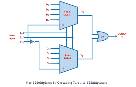
Fig. 8-to-1 Multiplexer By Cascading 4-to-1 Multiplexers
The truth table is shown in the below table. We get the output, and when MUX-1 is enabled and when MUX-2 enabled.
S0 | S1 | S2 | Y |
0 | 0 | 0 | D0 |
0 | 0 | 1 | D1 |
0 | 1 | 0 | D2 |
0 | 1 | 1 | D3 |
1 | 0 | 0 | D4 |
1 | 0 | 1 | D5 |
1 | 1 | 0 | D6 |
1 | 1 | 1 | D7 |
Advantages of a Multiplexer
The following are some of the benefits of using a Multiplexer:
1. A multiplexer cuts down on the number of wires that must be used. As a result, the circuit complexity and total cost are reduced.
2. Because it decreases the number of external wired connections, a multiplexer increases the reliability of digital systems.
3. MUX can be used to create a variety of combinational circuits.
4. The logic design is simplified by using a multiplexer.
5. The k-maps (Karnaugh map) and simplification are not required by the multiplexer.
Applications of a Multiplexer
Multiplexers can be used for a variety of purposes, including:
System of Communication
1. Multiplexers are used in communication systems as a data selector to choose one of several data inputs to broadcast many types of data (audio, video, etc.) at the same time. As a result, it improves the communication system's efficiency by allowing multiple types of data to be transmitted over a single transmission line.
2. Telecommunications networks
3. Multiplexers can be used in a telephone network to combine various audio streams into a single channel.
4. Memory in Computers
5. Multiplexers are used in computer memory to incorporate a huge quantity of data while reducing the number of copper wires needed to connect memory to other sections of the computer.
6. Satellite transmission from the computer system
7. Multiplexers are also used to send data from a spacecraft's or satellite's computer system to the earth via the "GPS" (Global Positioning System) and "GSM" (Global System for Mobile Communications) systems (Global System for Mobile Communication).
8. There are also the following applications:
9. Multiplexers can be used to build combinational logic circuits such as time and frequency multiplexing systems, as well as A/D and D/A converters.
10. Multiplexers can be utilised to implement multiple-variable Boolean functions.
In data acquisition systems, multiplexers are utilised.
Key takeaway:
- Multiplexing is a method for combining numerous data signals onto a single data channel.
- Analog multiplexing and digital multiplexing are two types of multiplexing.
- Analog multiplexing is used to combine analogue signals and is divided into two types: frequency division and wavelength division multiplexing.
- Only digital signals can be used in digital multiplexing, which is therefore categorised as time division multiplexing.
- Signals to be multiplexed are modulated over various carrier frequencies in frequency division multiplexing so that their bandwidth does not overlap.
- The sole distinction between wavelength division multiplexing and frequency division multiplexing is that WDM is utilised for fibre optic transmission.
- The signals to be multiplexed are divided into fixed-length time slots in time-division multiplexing.
3.2.1 Demultiplexer
A demultiplexer (also known as a demux) is a device that converts a single digital input line into one or more digital output lines. A 2n output demultiplexer contains n select lines that are used to choose which output line to transfer the input to. A data distributor is another name for a demultiplexer.
General-purpose logic can be implemented with demultiplexers. The demux becomes a decoder when the input is set to true.
The digital multiplexer is the inverse of the digital demultiplexer.
1 to 4 demultiplexer
Two select lines (S0, S1) are used in a 1 to 4 multiplexer to determine which of the four outputs (Y0 - Y3) is routed from the input (D). The following simplified truth table summarises its qualities.
Truth Table
S1 | S0 | Y3 | Y2 | Y1 | Y0 |
0 | 0 | 0 | 0 | 0 | D |
0 | 1 | 0 | 0 | D | 0 |
1 | 0 | 0 | D | 0 | 0 |
1 | 1 | D | 0 | 0 | 0 |
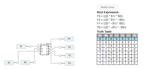
Notes:
● S1, S0 are the select inputs to change.
● Change the input and check to see if it's being routed to the desired output (Y0 - Y3)
● Smaller demultiplexers can be chained together to make larger demultiplexers. When you hover your mouse over the 1 to 4 DEMUX sub circuit, you'll notice that it's made up of three cascading 1 to 2 DEMUX.
● Demultiplexer 1 to 2
● One select line (S) is used in a 1 to 2 demultiplexer to identify which of the two outputs (Y0, Y1) is routed from the input (D). Its truth table is as follows:
Truth Table
S | Y1 | Y0 |
0 | 0 | D |
1 | D | 0 |
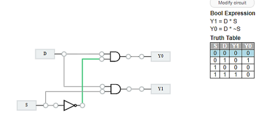
3.2.2 Demultiplexers
A demultiplexer, often known as a dmux, is a circuit with one input and multiple outputs. When a circuit wants to convey a signal to a group of devices, it uses it. This description sounds similar to the description given for a decoder, but a decoder is used to select among many devices while a demultiplexer is used to send a signal among many devices.
Demultiplexers are used frequently enough that they have their own schematic symbol (Figure below)
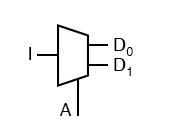
The truth table for a 1-to-2 demultiplexer is:
I | A | D0 | D1 |
0 | 0 | 0 | 0 |
0 | 1 | 0 | 0 |
1 | 0 | 1 | 0 |
1 | 1 | 0 | 1 |
We can easily define this circuit using our 1-to-2 decoder as part of the circuit:

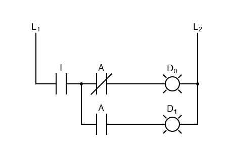
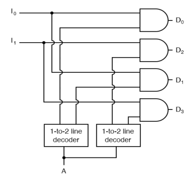
There are two distinct ways to expand this circuit. You can either increase the number of signals that are sent or the number of inputs that are passed through. A larger line decoder is all that is required to increase the number of inputs that are passed through. It's even easy to increase the quantity of signals sent out.
A “two-bit 1-to-2 demultiplexer,” for example, is a device that passes one set of two signals among four signals. Its circuit is as follows:
Both 8x1 Multiplexers use the same selection lines, s2, s1, and s0. I15 to I8 are the data inputs of the upper 8x1 Multiplexer, whereas I7 to I0 are the data inputs of the lower 8x1 Multiplexer. As a result, each 8x1 Multiplexer generates an output based on the selection lines' values, s2, s1, and s0.
The outputs of the first stage's 8x1 Multiplexers are used as inputs to the second stage's 2x1 Multiplexer. 2x1 Multiplexer receives the other selection line, s3.
If s3 is zero, the output of the 2x1 Multiplexer will be one of the 8 inputs Is7 to I0, which are determined by the values of the selection lines s2, s1, and s0.
● If s3 is one, the output of the 2x1 Multiplexer will be one of the eight inputs I15 to I8, dependent on the values of the selection lines s2, s1, and s0.
● As a result, a 16x1 Multiplexer is created by combining two 8x1 Multiplexers and one 2x1 Multiplexer. Alternatively, you can write the circuit as, shows that two one-bit 1-to-2 demultiplexers might be used without affecting the intended behaviour.
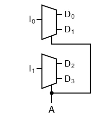

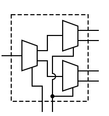
As seen below, a 1-to-4 demultiplexer can be simply constructed from 1-to-2 demultiplexers.
3.3.1 Decoder
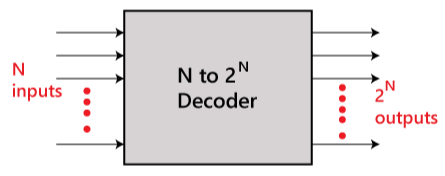
Decoders are combinational circuits that convert binary information into 2N output lines. N input lines are used to transfer the binary information. The binary information is encoded in a 2N-bit code on the output lines. To put it another way, the Decoder reverses the Encoder's action. For simplicity, just one input line is active at a time. The binary information is comparable to the 2N-bit output code.
2 to 4 line decoder:
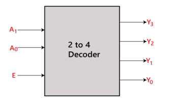
There are three inputs (A0, A1, and E) and four outputs (Y0, Y1, Y2, and Y3) in the two to four line decoder. When the enable 'E' is set to 1, one of these four outputs will be 1 for each combination of inputs. The 2 to 4 line decoder's block diagram and truth table are shown below.
Block Diagram:
Truth Table:
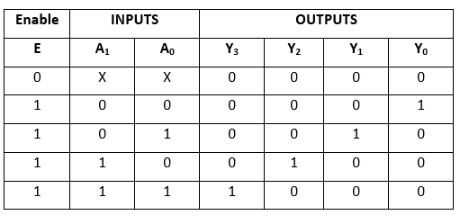
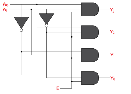
The logical expression of the term Y0, Y0, Y2, and Y3 is as follows:
Y3=E.A1.A0
Y2=E.A1.A0'
Y1=E.A1'.A0
Y0=E.A1'.A0'
3 to 8 line decoder:
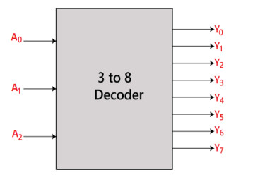
Binary to Octal Decoder is another name for the 3 to 8 line decoder. There are eight outputs in a 3 to 8 line decoder, including Y0, Y1, Y2, Y3, Y4, Y5, Y6, and Y7, as well as three outputs, namely A0, A1, and A2. The enable input 'E' is used in this circuit. When enable 'E' is set to 1, one of these four outputs will be 1, just like a 2 to 4 line decoder. The 3 to 8 line encoder's block diagram and truth table are shown below.
Block Diagram:
Truth Table:
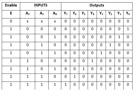
The logical expression of the term Y0, Y1, Y2, Y3, Y4, Y5, Y6, and Y7 is as follows:
Y0=A0'.A1'.A2'
Y1=A0.A1'.A2'
Y2=A0'.A1.A2'
Y3=A0.A1.A2'
Y4=A0'.A1'.A2
Y5=A0.A1'.A2
Y6=A0'.A1.A2
Y7=A0.A1.A2
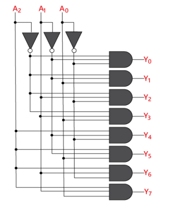
Logical circuit of the above expressions is given below:
8 to 16 line Decoder
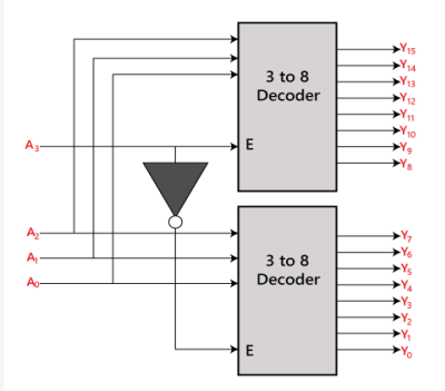
There are 16 outputs (Y0, Y1, Y2,......, Y16) and four inputs (A0, A1, A2, and A3) in the 4 to 16 line decoder. Either a 2 to 4 decoder or a 3 to 8 decoder can be used to build a 3 to 16 line decoder. To calculate the required number of lower-order decoders, use the formula below.
Required number of lower order decoders=m2/m1
m1 = 8
m2 = 16
Required number of 3 to 8 decoders= =2
=2
Block Diagram:
Truth Table:
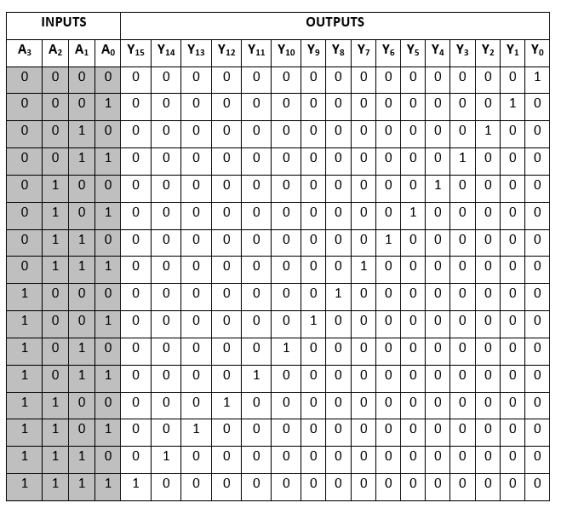
The logical expression of the term A0, A1, A2,…, A15 are as follows:
Y0=A0'.A1'.A2'.A3'
Y1=A0'.A1'.A2'.A3
Y2=A0'.A1'.A2.A3'
Y3=A0'.A1'.A2.A3
Y4=A0'.A1.A2'.A3'
Y5=A0'.A1.A2'.A3
Y6=A0'.A1.A2.A3'
Y7=A0'.A1.A2.A3
Y8=A0.A1'.A2'.A3'
Y9=A0.A1'.A2'.A3
Y10=A0.A1'.A2.A3'
Y11=A0.A1'.A2.A3
Y12=A0.A1.A2'.A3'
Y13=A0.A1.A2'.A3
Y14=A0.A1.A2.A3'
Y15=A0.A1.A2'.A3
3.3.2 Types of Binary Decoders, Applications
In essence, a Decoder is a combinational logic circuit that translates coded input to coded outputs when both of these are distinct. The term "decoder" refers to a device that converts coded data from one format to another. As a result, the input code has less bits than the output code word.
A digital decoder is a device that translates a set of digital signals into decimal code. Prior to the advent of an encoder, a decoder was a regularly utilised circuit. After the information is encoded by encoders, it is decoded for user interface in most output devices such as monitors, calculator displays, printers, and so on. We'll look at numerous sorts of binary decoders in this article.
Binary Decoders
A binary decoder is a multi-input, multi-output combinational circuit that converts a binary code of n input lines into a one out of 2n output code. When an n-bit input value is needed to activate exactly one of 2n outputs, these are employed.
The diagram below depicts the overall structure of a binary decoder, which accepts encoded data on n input lines and produces output on 2n potential output lines.
Enable inputs are typically included with decoders to activate the decoded output based on data inputs. In BCD coding, for example, the four bit combinations 0000 through 1001 are sufficient to represent the decimal numbers 0 to 9.
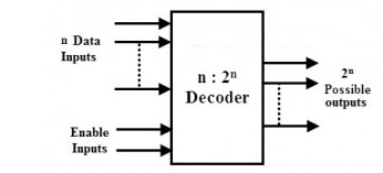
The inputs of a binary code can be 2-bit, 3-bit, or 4-bit codes, depending on the number of input lines. When it receives n inputs and there are 2n lines available, it activates one of its outputs by deactivating (making logic 0) the other inputs.
The number of bits in output code is usually greater than the number of bits in the input code. 2-to-4 decoders, 3-to-8 decoders, and 4-to-16 line binary decoders are the most often used practical binary decoders.
2-to-4 Binary Decoder
Two inputs are decoded into four outputs in a 2-to-4 binary decoder, which has two input lines and four output lines. At any one time, only one output is active, while the others are kept at logic 0, and the output that is kept active or high is controlled by the two binary inputs A and B.
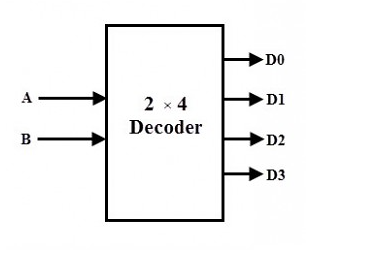
The truth table for a 2-to-4 decoder is shown in the diagram below. If the enable input EN is active high (EN = 1), the outputs Y0 through Y3 are active high for a particular input. When both A and B are low (or A= B= 0), the output Y0 is active or high, while all other outputs are low.
The output Y1 will be active when A = 0 and B = 1, and when A = 1 and B = 0, the output Y2 will be active. When both inputs are high, the output Y3 is high as well. All outputs will be set to zero if the enable bit is set to zero. This link between inputs and outputs is clearly depicted in the truth table below.
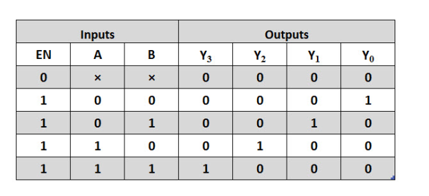
From the above truth table we can obtain Boolean expression for the each output as

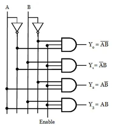
Basic logic gates can be used to implement these expressions. As a result, the 2-to-4 line decoder logic circuit architecture is shown below, which is built using NOT and AND gates. The complement of inputs is provided by two NOT gates or inverters.
Each AND gate is coupled to a common enable line, so that when EN=0, all outputs are zero, and when EN=1, outputs are created depending on the inputs A and B. Each output reflects one of the two input variables' minterms.
It's also possible to create a 2-to-4 decoder utilising NAND gates and a truth table, as shown in the diagram below. This is built on the notion of using maximum terms as outputs. We must employ NAND gates, which operate as inverters, to generate the minterms. Y0 will be zero if both inputs are zero (A = B = 0), Y1 will be 1 if A = 0 and B= 1, and so on.
As a result, for each combination of inputs at any given time, only one output will be low, while all other outputs will be high. This sort of decoder is also available in IC form, allowing for the creation of 3 to 8, 4 to 16, and 5 to 32 decoders, depending on the application requirements.
3-to-8 Decoder
Three inputs are processed into eight outputs in a 3-to-8 decoder. It has three inputs as A, B, and C and eight output from Y0 through Y7. Only one of the eight outputs is chosen based on the combinations of the three inputs.
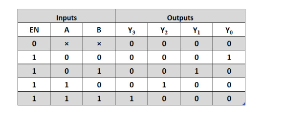
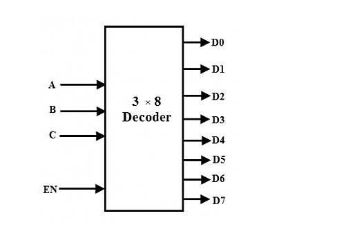
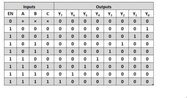
The truth table of a 3-to-8 decoder is shown in the diagram below. The decoded output is activated using the enable input, which is dependent on the input combinations A, B, and C. If A = B=1 and C= 0, then Y6 is 1 and all other outputs are zero. Minterms represent each output equation in the truth table and are given as
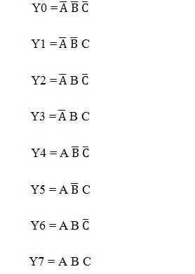
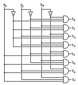
Three NOT gates and eight AND gates can be used to create the 3-to-8 decoder circuit utilising the following min term expressions for each output. The complement of the input is provided by each NOT gate, and one of the minterms is generated by each AND gate.
Also, if input is enabled, the decoded output is activated based on the input data. This decoder's logic diagram is presented below.
This decoder is also known as a 1-of-8 decoder because only one of the eight outputs is high at any one time for a given input combination. Assume that when ABC = 011, only AND gate 4 has all inputs high, resulting in Y3 being high.
Also known as a binary-to-octal decoder, it converts 3-bit binary values at the input to eight digits at the output (which is equal to the octal number system).
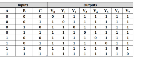
It's also feasible to use max terms to represent each output equation. In this situation, the logic circuit performs inversion rather than the circuit with min terms. The truth table of a 3-to-8 line decoder utilising NAND gates is shown in the diagram below. Each of the table's outputs is a maximum term representation.
Only one output will be low at any one time, while all other outputs will be high. When A=B=1 and C=0, for example, the output Y6 is zero and all other outputs are high, as indicated in the diagram below.
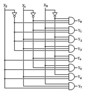
A 3-to-8 line decoder is created utilising three NAND gates and three NOT gates, as shown in the table above. As indicated in the diagram below, NOT gates generate the complement of the input, while NAND gates generate the maximum terms of each output.
4-to-16 Decoder
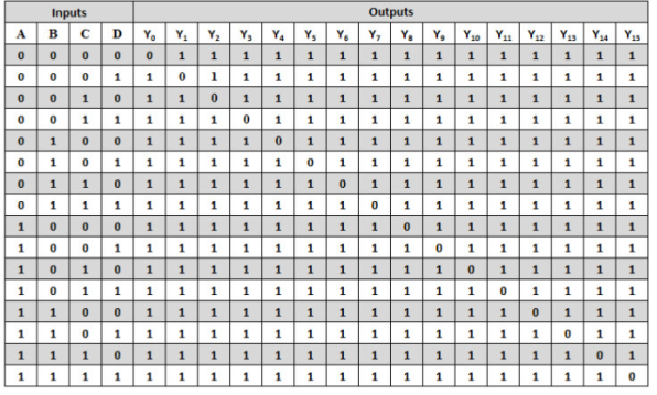
A 4-to-16 decoder has four inputs and sixteen outputs. Like all of the previous decoders, just one output will be low at any given moment, while all other outputs will be high (using maxterms).
This type of decoder's truth table is illustrated below. If the decoder's input is 1000, output Y8 will be low, while all other outputs will be high, as illustrated in the diagram. This will continue to be the case for all input combinations.
A 4-to-16 decoder can be built using 4 NOT gates and 16 decoding NAND gates, as shown in the truth table above. A total of sixteen (24 = 16) decoding gates are required to decode all conceivable combinations of four bits input.
It's worth noting that all of the NAND gates used in this circuit provide active low outputs, as seen in the diagram.
These decoders are also known as 1-of-16 decoders since they select one of 16 outputs based on the input combination. This sort of decoder is also known as a binary-to-hexadecimal decoder since its output reflects the sixteen digits as hexadecimal number system.
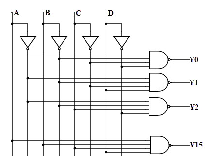
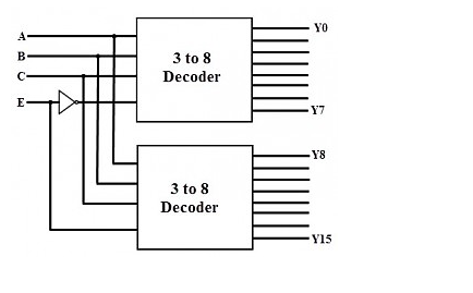
The enable input of a decoder can be used to combine or cascade two or more decoders to build a decoder with a higher number of input bits. Below is a diagram of a cascade combination of two 3-to-8 line decoders. It has four inputs (A, B, C, and Enable E), as well as 16 outputs (Y0 to Y7).
One of the input variables is utilised as the first 3-to-4 decoder's enable input, and the same input is complemented and connected as the second decoder's enable input. The most significant input variable determines which decoder is enabled, and other input variables are provided to each decoder.
When the enable input is 0, the top decoder is turned on and the other is turned off. The minterms 0000 to 0111 are generated by the top decoder's eight outputs. When enable is set to 1, the lower decoder is enabled and the top decoder is disabled. As a result, the bottom decoder outputs provide minterms ranging from 1000 to 1111.
Applications of Decoders
Decoders are commonly employed in applications where a specific output or group of outputs is only triggered when a specified combination of input levels occurs. The outputs of a register or counter are frequently used to supply these input values.
The outputs will be engaged in a sequential order if the counter or register continually pulses the decoder inputs. These outputs can also be used as timing or sequencing signals to switch devices at specific moments.
Binary to Decimal Decoder
The decimal digit matching to a certain input combination is obtained using decoders. To represent the 0 to 9 decimal digits, a BCD number requires four binary digits, resulting in four input lines. It has ten output lines, each corresponding to a decimal digit from 0 to 9.
TA 1 to 10 decoder is another name for this type of decoder. The output will be enabled corresponding to the decimal equivalent of the input combination for a certain input combination.
Address Decoders
A decoder is commonly used to decode a specific memory address in the computer memory system, among other things. Decoders receive the CPU-generated address code, which is a combination of address bits for a given memory location.
Several memory ICs are coupled in a memory system, each with its own unique address to distinguish it from other memory locations.
In such cases a decoder built in the memory ICs circuitry, is used to select a memory IC in response to a range of addresses by decoding the most significant bits of the systems address, thereby a particular memory location or IC is selected.
Memory ICs or chips are placed in many banks in a more complicated memory system. These banks must be selected concurrently or individually when the CPU needs to access one or more bytes at a time.
In such circumstances, multiple decoders must be turned on. For this, cascaded decoders are employed or, more typically, programmable logic devices are utilised instead of decoders.
3.3.5 Decoders and Multiplexers
Decoders
A decoder is a circuit with n inputs and 2n outputs that outputs the binary number represented by the inputs as 1 on the wire. A 2-4 decoder, for example, may be illustrated as follows:

And its truth table (again, really four truth tables, one for each output) is:
i1 | i0 | d3 | d2 | d1 | d0 |
0 | 0 | 0 | 0 | 0 | 1 |
0 | 1 | 0 | 0 | 1 | 0 |
1 | 0 | 0 | 1 | 0 | 0 |
1 | 1 | 1 | 0 | 0 | 0 |
We can observe right away that
|
|
| ||||||
|
|
| ||||||
|
|
| ||||||
|
|
|
i.e. each of the d outputs corresponds to one of the four minterms.
The Circuit of the Decoder
The 2-4 decoder is implemented in the following circuit, which creates all four minterms from two inputs.
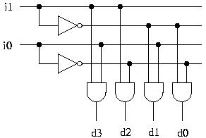
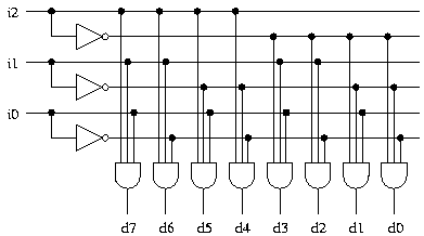
In the same approach, larger decoders can be implemented. A 3-8 decoder can be found here.
Decoder-equipped traffic lights
The circuit that generates traffic light combinations using a 2-4 decoder is as follows.

We don't have to worry about invalid inputs being provided to the circuit any longer.
To complete the traffic light controller, we just need to make the inputs i0 and i1 cycle through the binary representations of the numbers 0�3. Later in the course, we'll look at how to do this.
Standard components include decoders of various sizes.
Decoders that work with Enable
An additional input called Enable is usually found on a conventional decoder.

When the Enable input is set to 1, output is created; otherwise, all outputs are 0. The Enable input is sent into the AND gates, which create the outputs, requiring only a minor adjustment in the implementation.
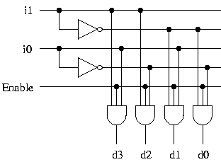
This is how the Enable input works in many components. The Enable input is active high at times and active low at other times.
3.4.1 Encoders
Encoders are a type of combinational circuit that converts binary data into N output lines. The binary data is sent in the form of 2N input lines. The binary information's N-bit coding is defined by the output lines. To put it another way, the Encoder reverses the Decoder's action. For simplicity, just one input line is active at a time. The binary information is equivalent to the N-bit output code.
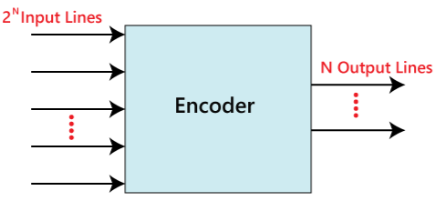
There are various types of encoders which are as follows:
3 to 2 line Encoder:
There are four inputs in a 4 to 2 line encoder, namely Y0, Y1, Y2, and Y3, and two outputs, namely A0 and A1. To get the respective binary code on the output side, one input line at a time is set to true in a 4-input line. The 4 to 2 line encoder's block diagram and truth table are shown below.
Block Diagram:
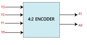
Truth Table:
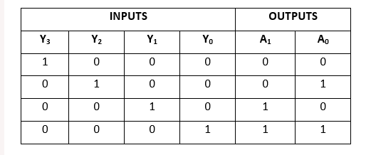
The following is the logical expression of the terms A0 and A1:
A1=Y3+Y2
A0=Y3+Y1
The following is the logical circuit for the above expressions:
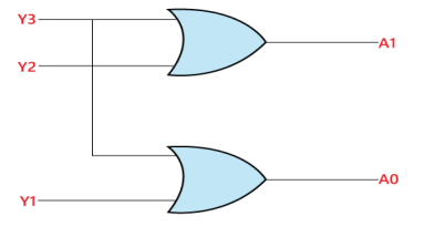
8 to 3 line Encoder:
Octal to Binary Encoder is another name for the 8 to 3 line encoder. There are eight inputs (Y0, Y1, Y2, Y3, Y4, Y5, Y6, and Y7) and three outputs (A0, A1, and A2) in an 8 to 3 line encoder. One input line at a time is set to true in an 8-input line to retrieve the corresponding binary code on the output side. The 8 to 3 line encoder's block diagram and truth table are shown below.
Block Diagram:
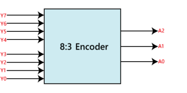
Truth Table:
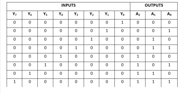
The logical expression of the term A0, A1, and A2 are as follows:
A2=Y4+Y5+Y6+Y7
A1=Y2+Y3+Y6+Y7
A0=Y7+Y5+Y3+Y1
Logical circuit of the above expressions is given below:
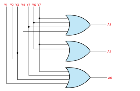
Decimal to BCD Encoder
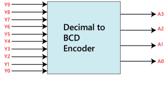
The 10 to 4 line encoder is another name for the Octal to Binary Encoder. In 10 to 4 line encoder, there are total of ten inputs, i.e., Y0, Y1, Y2, Y3, Y4, Y5, Y6, Y7, Y8, and Y9 and four outputs, i.e., A0, A1, A2, and A3. To get the respective BCD code on the output side, one input line at a time is set to true in a 10-input line array. The decimal to BCD encoder's block diagram and truth table are shown below.
Block Diagram:
Truth Table:
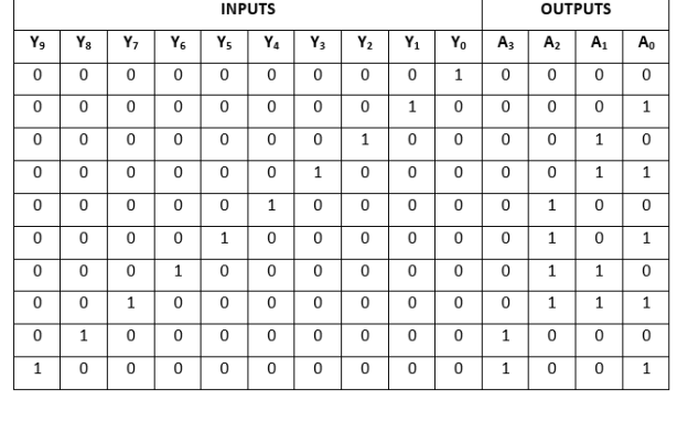
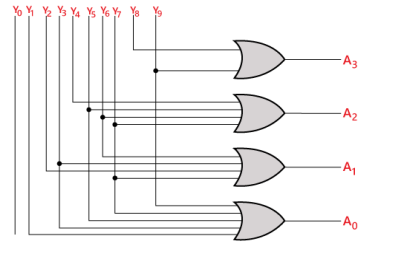
The logical expression of the term A0, A1, A2, and A3 is as follows:
A3 = Y9 + Y8
A2 = Y7 + Y6 + Y5 +Y4
A1 = Y7 + Y6 + Y3 +Y2
A0 = Y9 + Y7 +Y5 +Y3 + Y1
Logical circuit of the above expressions is given below:
3.4.2 Priority Encoder:
4 to 2 line Priority Encoder:
There are four inputs in this priority encoder: Y0, Y1, Y2, and Y3, as well as two outputs: A0 and A1. The Y3 has high priority inputs, while the Y0 has low priority inputs. When more than one input is '1' at the same time, the output is the (binary) code that corresponds to the input with the greater priority. The truth table for the 4 to 2 line priority encoder is shown below.
Truth Table:
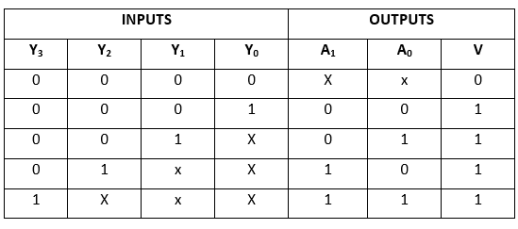
The logical expression of the term A0 and A1 can be found using K-map as:
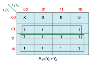
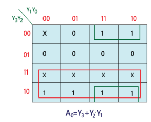
A1=Y3+Y2
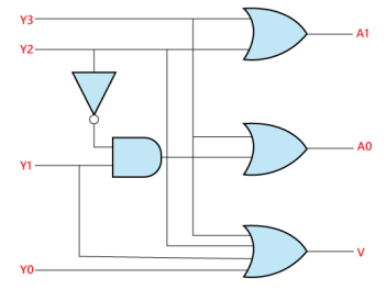
A0=Y3+Y2'.Y1
Logical circuit of the above expressions is given below:
8-to-3 Bit Priority Encoder
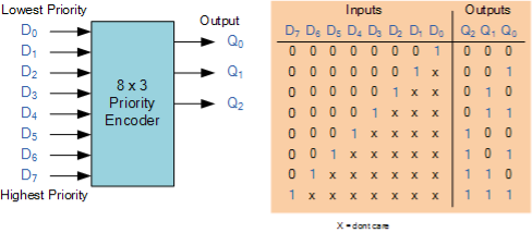
The TTL 74LS148 is an 8-to-3 bit priority encoder with eight active LOW (logic “0”) inputs and gives a 3-bit code of the highest ranking input at its output.
Priority encoders produce the highest order input first. For example, if input lines “D2,” “D3,” and “D5” are all applied at the same time, the output code for input “D5” (“101”) would be used because it has the highest rank of the three inputs. After removing input “D5,” the highest output code would be for input “D3” (“011”), and so on.
The truth table for a 8-to-3 bit priority encoder is given as:
Digital Inputs | Binary Output | |||||||||
D7 | D6 | D5 | D4 | D3 | D2 | D1 | D0 | Q2 | Q1 | Q0 |
0 | 0 | 0 | 0 | 0 | 0 | 0 | 1 | 0 | 0 | 0 |
0 | 0 | 0 | 0 | 0 | 0 | 1 | X | 0 | 0 | 1 |
0 | 0 | 0 | 0 | 0 | 1 | X | X | 0 | 1 | 0 |
0 | 0 | 0 | 0 | 1 | X | X | X | 0 | 1 | 1 |
0 | 0 | 0 | 1 | X | X | X | X | 1 | 0 | 0 |
0 | 0 | 1 | X | X | X | X | X | 1 | 0 | 1 |
0 | 1 | X | X | X | X | X | X | 1 | 1 | 0 |
1 | X | X | X | X | X | X | X | 1 | 1 | 1 |
Where X = "don't care," it can be at either a logic "0" or a logic "1" level.
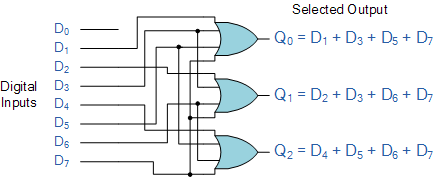
The Boolean expression for the encoder above with data inputs D0 to D7 and outputs Q0, Q1, Q2 is given by this truth table:
Output Q0

Output Q1

Output Q2

Then the final Boolean expression for the priority encoder including the zero inputs is defined as:
Output Expression of the Priority Encoder

In practise, these zero inputs would be disregarded, allowing the final Boolean expression for the 8-to-3 priority encoder's outputs to be implemented. Individual OR gates can be used to create a simple encoder from the expression above.
Digital Encoder using Logic Gates
Digital Encoder Applications
1. Keyboard Encoder
Priority encoders can be used in circuits or applications with many inputs to reduce the number of wires required. Assume that a microcomputer needs to read the 104 keys on a normal QWERTY keyboard, where only one key is touched at a time, either "HIGH" or "LOW."
One option is to link all 104 wires from the individual keys on the keyboard to the computer's input directly, although this is difficult for a tiny home PC. Another, better option is to use a priority encoder to connect the keyboard to the computer.
To represent each key or character on the keyboard, the 104 separate buttons or keys could be converted into a conventional ASCII code of only 7 bits (0 to 127 decimal) and then directly input to the computer as a considerably smaller 7-bit B.C.D code. To do so, keypad encoders like the 74C923 20-key encoder are available.
2. Positional Encoders
Magnetic positional control, such as that used on ships or for robotic arm positioning, is another more widespread application. A 74LS148 8-to-3 line priority encoder, for example, converts the angular or rotational position of a compass into a digital code that is then entered to the systems computer to provide navigational data, and an example of a simple 8 position to 3-bit output compass encoder is shown below. To show the needles' angular location, magnets and reed switches could be employed at each compass point.
3. Priority Encoder Navigation
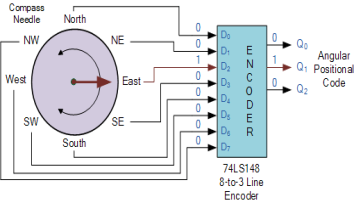
Compass Direction | Binary Output | ||
Q0 | Q1 | Q2 | |
North | 0 | 0 | 0 |
North-East | 0 | 0 | 1 |
East | 0 | 1 | 0 |
South-East | 0 | 1 | 1 |
South | 1 | 0 | 0 |
South-West | 1 | 0 | 1 |
West | 1 | 1 | 0 |
North-West | 1 | 1 | 1 |
4. Interrupt Requests
Detecting interruptions in microprocessor applications could be another application for Priority Encoders. The microprocessor here uses interrupts to allow peripheral devices like the disc drive, scanner, mouse, or printer to communicate with it. However, because the microprocessor can only “talk” to one peripheral device at a time, it needs a way of knowing when a particular peripheral device wants to communicate with it.
The processor accomplishes this by assigning priority to all peripheral devices via "Interrupt Requests" or "IRQ" signals, ensuring that the most critical peripheral device is handled first. The priority of the devices will be determined by how they are connected to the priority encoder.
IRQ Number | Typical Use | Description |
IRQ 0 | System timer | Internal System Timer. |
IRQ 1 | Keyboard | Keyboard Controller. |
IRQ 3 | COM2 & COM4 | Second and Fourth Serial Port. |
IRQ 4 | COM1 & COM3 | First and Third Serial Port. |
IRQ 5 | Sound | Sound Card. |
IRQ 6 | Floppy disk | Floppy Disk Controller. |
IRQ 7 | Parallel port | Parallel Printer. |
IRQ 12 | Mouse | PS/2 Mouse. |
IRQ 14 | Primary IDE | Primary Hard Disk Controller. |
IRQ 15 | Secondary IDE | Secondary Hard Disk Controller. |
Because creating such a system with standard priority encoders like the 74LS148 requires additional logic circuits, purpose-built integrated circuits like the 8259 Programmable Priority Interrupt Controller are available.
Uses of Encoders:
1. In all digital systems, these systems are relatively simple to operate.
2. To convert a decimal value to a binary value, encoders are used. The goal is to complete a binary operation like addition, subtraction, multiplication, and so on.
Key takeaway:
• Learn about the new iC-PVS and how to configure it for various magnetic absolute encoder applications.
• View live demonstrations: stand-alone iC-PVS and performance system with iC-TW29 • Learn how to combine iC-PVS and iC-TW29 to produce high-resolution absolute encoders
3.5.1 Binary Adder
Addition is the most fundamental arithmetic operation. The binary adder is a circuit that performs the addition of two binary numbers. Let's start with an adder that adds two bits together.
Half Adder
A half adder is a combinational circuit that performs the addition of two single-bit binary values A and B. It has two outputs: sum (S) and carry (C).
Half adder's truth table is provided below.
Inputs | Outputs | ||
A | B | C | S |
0 | 0 | 0 | 0 |
0 | 1 | 0 | 1 |
1 | 0 | 0 | 1 |
1 | 1 | 1 | 0 |
When we add two bits together, the resultant sum can have decimal values ranging from 0 to 2. In binary, the decimal numbers 0 and 1 can be represented by a single bit. However, we can't express the decimal numeral 2 in binary with a single bit. As a result, we'll need two bits to represent it in binary.
Let S be the least significant bit of the final total, and C be the most significant bit. Carry is 0 for the first three input combinations, and S is either zero or one depending on the amount of ones present at the inputs. However, because the final sum is two, carry, C, is one and sum, S, is zero for the last combination of inputs.
From Truth table, we can directly write the Boolean functions for each output as
S=A⊕BS=A⊕B
C=AB
The above functionalities can be implemented using a 2-input Ex-OR gate and a 2-input AND gate. The circuit schematic for a half adder may be found in the diagram below.
A two-input Ex-OR gate and a two-input AND gate create sum, S, and carry, C, respectively, in the above circuit. As a result, Half-adder does a two-bit addition.
Full Adder
The full adder is a combinational circuit that adds the three bits A, B, and Cin. Where A and B are two parallel significant bits, and Cin is the carry bit generated in the preceding stage. This Full adder also has two outputs that are comparable to Half adders: sum, S, and carry, Cout.
The Truth table of Full adder is shown below.
Inputs | Outputs | |||
A | B | Cin | Cout | S |
0 | 0 | 0 | 0 | 0 |
0 | 0 | 1 | 0 | 1 |
0 | 1 | 0 | 0 | 1 |
0 | 1 | 1 | 1 | 0 |
1 | 0 | 0 | 0 | 1 |
1 | 0 | 1 | 1 | 0 |
1 | 1 | 0 | 1 | 0 |
1 | 1 | 1 | 1 | 1 |
When we add three bits together, the resultant sum can have decimal values ranging from 0 to 3. In binary, the decimal numbers 0 and 1 can be represented by a single bit. However, we can't express the decimal numbers 2 and 3 in binary with a single bit. As a result, two bits are required to represent those two decimal digits in binary.
Let S be the least significant bit of the resultant total, and Cout be the most significant bit of the subsequent total. It's simple to populate the values of outputs in the truth table for any combination of inputs. Simply count the number of ones at the inputs and write the binary equivalent at the outputs. The Full adder truth table is the same as the Half adder truth table if Cin is equal to zero.
We will get the following Boolean functions for each output after simplification.
S=A⊕B⊕CinS=A⊕B⊕Cin
Cout=AB+(A⊕B)cincout=AB+(A⊕B)cin
When an odd number of ones are present at the inputs, the sum, S, equals one. We already know that the Ex-OR gate generates an output, which is a strange function. To produce sum, S, we can use either two 2-input Ex-OR gates or one 3-input Ex-OR gate. Two 2-input AND gates and one OR gate can be used to construct carry, Cout. The circuit diagram for a full adder can be found in the diagram.
This adder is called a Full adder since it takes two Half adders and one OR gate to implement one Full adder. Full adder becomes Half adder if Cin is zero. We may simply test it using the circuit schematic above or the Boolean functions of Full adder outputs.
4-bit Binary Adder
The addition of two 4-bit values is performed using the 4-bit binary adder. Let A=A3A2A1A0A=A3A2A1A0 and B=B3B2B1B0B=B3B2B1B0 be the 4-bit binary numbers. The 4-bit binary adder can be implemented in one of two ways.
- For the addition of two least significant bits, use one Half adder, and three full adders for the addition of three higher significant bits.
- For consistency, use four full adders. Because the initial carry Cin is zero, the Half adder is utilised to add the least significant bits instead of the Full adder.
- We examined the second method for the time being. The following diagram depicts the block diagram of a 4-bit binary adder.
- The four full adders are cascaded here. Each Full adder receives the bits from two parallel inputs A and B. The carry input of the next higher order Full adder will be the carry output of the previous Full adder. The output sum of this 4-bit binary adder has a maximum of 5 bits. As a result, the MSB will carry out the last step Full adder.
- We can create any higher order binary adder by cascading the needed number of Full adders in this fashion. Because the carry propagates ripples from one stage to the next, this binary adder is also known as a ripple carry binary adder.
Binary Subtractor
The Binary subtractor is a circuit that conducts the subtraction of two binary numbers. The binary subtractor can be implemented using one of the two approaches below.
2's complement approach with cascade full subtractors
By cascading ‘n' Full subtractors, we can create an n-bit binary subtractor in the first approach. So, similar to Half adder and Full adder, you may start by implementing Half subtractor and Full subtractor. Then, by cascading ‘n' Full subtractors, you can create an n-bit binary subtractor. So, for binary addition and subtraction of two binary numbers, we'll have two different circuits.
In the second way, we can subtract two binary values with the same binary adder by making a few changes to the second input. As a result, a binary addition operation is performed internally, but the output is resulting subtraction.
The subtraction of two binary values A and B can be expressed as, as we know.
A−B=A+(2′scomplimentofB)
⇒A−B=A+(1′scomplimentofB)
4-bit Binary Subtract
Two 4-bit values are subtracted using the 4-bit binary subtractor. Let A=A3A2A1A0A=A3A2A1A0 and B=B3B2B1B0B=B3B2B1B0 be the 4bit binary numbers. The functioning of the 4-bit Binary subtractor is similar to that of the 4-bit Binary adder on the inside. When the normal bits of binary number A, the complemented bits of binary number B, and the initial carry borrow, Cin are applied as one to a 4-bit Binary adder, the result is a 4-bit Binary subtractor. The following diagram depicts the block diagram of a 4-bit binary subtractor.
This 4-bit binary subtractor generates an output with a maximum of 5 bits. If Binary number A is bigger than Binary number B, the output's MSB is zero, and the remaining bits contain the A-B magnitude. The output's MSB is one if Binary number A is less than Binary number B. To find the magnitude of A-B, take the 2's complement of the output.
By cascading the requisite number of Full adders with the relevant modifications, we may create any higher order binary subtractor.
Binary Adder / Subtractor
The Binary Adder / Subtractor is a circuit that may be used to do either addition or subtraction of two binary values at any time. Both the Binary adder and the Binary subtractor have a cascaded set of Full adders. Both the Binary adder and Binary subtractor use the input bits of binary number A directly.
The inputs of Full adders differ from those of Binary adder and Binary subtractor in two ways.
- In a Binary adder, the input bits of binary number B are applied directly to Full adders, whereas in a Binary subtractor, the complemented bits of binary number B are applied to Full adders.
- In a 4-bit Binary adder, the initial carry, C0 = 0, is used, whereas in a 4-bit Binary subtractor, the initial carry borrow, C0 = 1, is used.
When the other input is zero, a 2-input Ex-OR gate produces an output that is the same as the first input. When the other input is one, it creates an output that is the complement of the first.
As a result, we can use the binary number B's input bits in 2-input Ex-OR gates. C0 is the other input for all of these Ex-OR gates. Ex-OR gates create either the normal or complemented bits of binary number B depending on the value of C0.
4-bit Binary Adder / Subtractor
Based on the value of the initial carry or borrow, C0, the 4-bit binary adder / subtractor performs either addition or subtraction of two 4-bit values. Let A=A3A2A1A0A=A3A2A1A0 and B=B3B2B1B0B=B3B2B1B0 be the 4-bit binary numbers. The 4-bit Binary adder / subtractor operates similarly to the 4-bit Binary adder and 4-bit Binary subtractor.
Apply the regular bits of binary numbers A and B, as well as the initial carry or borrow, C0, to a 4-bit binary adder from the outside. The following graphic depicts the block diagram of a 4-bit binary adder / subtractor.
Each full adder receives the regular bits of binary numbers A and B if the starting carry, C0, is zero. As a result, the 4-bit binary adder/subtractor generates an output that is the sum of two binary values A and B.
Each full adder receives the normal bits of binary number A and the complemented bits of binary number B if the initial borrow, C0, is one. As a result, the 4-bit binary adder / subtractor outputs the subtraction of two binary values A & B.
As a result, the same circuit may be used to add and subtract two binary values with the use of extra Ex-OR gates.
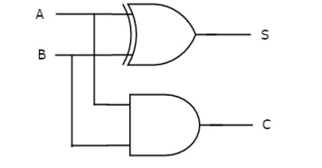
A two-input Ex-OR gate and a two-input AND gate create sum, S, and carry, C, respectively, in the above circuit. As a result, Half-adder does a two-bit addition.
Full Adder
The full adder is a combinational circuit that adds the three bits A, B, and Cin. Where A and B are two parallel significant bits, and Cin is the carry bit generated in the preceding stage. This Full adder also has two outputs that are comparable to Half adders: sum, S, and carry, Cout.
The Truth table of Full adder is shown below.
Inputs | Outputs | |||
A | B | Cin | Cout | S |
0 | 0 | 0 | 0 | 0 |
0 | 0 | 1 | 0 | 1 |
0 | 1 | 0 | 0 | 1 |
0 | 1 | 1 | 1 | 0 |
1 | 0 | 0 | 0 | 1 |
1 | 0 | 1 | 1 | 0 |
1 | 1 | 0 | 1 | 0 |
1 | 1 | 1 | 1 | 1 |
When we add three bits together, the resultant sum can have decimal values ranging from 0 to 3. In binary, the decimal numbers 0 and 1 can be represented by a single bit. However, we can't express the decimal numbers 2 and 3 in binary with a single bit. As a result, two bits are required to represent those two decimal digits in binary.
Let S be the least significant bit of the resultant total, and Cout be the most significant bit of the subsequent total. It's simple to populate the values of outputs in the truth table for any combination of inputs. Simply count the number of ones at the inputs and write the binary equivalent at the outputs. The Full adder truth table is the same as the Half adder truth table if Cin is equal to zero.
We will get the following Boolean functions for each output after simplification.
S=A⊕B⊕CinS=A⊕B⊕Cin
Cout=AB+(A⊕B)cincout=AB+(A⊕B)cin
When an odd number of ones are present at the inputs, the sum, S, equals one. We already know that the Ex-OR gate generates an output, which is a strange function. To produce sum, S, we can use either two 2-input Ex-OR gates or one 3-input Ex-OR gate. Two 2-input AND gates and one OR gate can be used to construct carry, Cout. The circuit diagram for a full adder can be found in the diagram below.
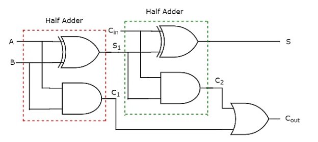
This adder is called a Full adder since it takes two Half adders and one OR gate to implement one Full adder. Full adder becomes Half adder if Cin is zero. We may simply test it using the circuit schematic above or the Boolean functions of Full adder outputs.
4-bit Binary Adder
The addition of two 4-bit values is performed using the 4-bit binary adder. Let A=A3A2A1A0A=A3A2A1A0 and B=B3B2B1B0B=B3B2B1B0 be the 4-bit binary numbers. The 4-bit binary adder can be implemented in one of two ways.
- For the addition of two least significant bits, use one Half adder, and three full adders for the addition of three higher significant bits.
- For consistency, use four full adders. Because the initial carry Cin is zero, the Half adder is utilised to add the least significant bits instead of the Full adder.
- We examined the second method for the time being. The following diagram depicts the block diagram of a 4-bit binary adder.
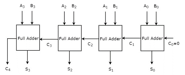
The four full adders are cascaded here. Each Full adder receives the bits from two parallel inputs A and B. The carry input of the next higher order Full adder will be the carry output of the previous Full adder. The output sum of this 4-bit binary adder has a maximum of 5 bits. As a result, the MSB will carry out the last step Full adder.
We can create any higher order binary adder by cascading the needed number of Full adders in this fashion. Because the carry propagates ripplesripples from one stage to the next, this binary adder is also known as a ripple carry binarybinary adder.
3.5.3 Binary arithmetic circuits
Introduction
The problem of binary arithmetic is a combinatorial one. It may appear straightforward to create circuits for binary arithmetic using the methods we've already seen for creating combinatorial circuits.
There is, however, an issue. It turns out that the traditional method of building such circuits consumes much too many gates. We need to look for alternative solutions.
Addition of binary integers
We can forego our earlier criteria for circuit depth in order to use fewer gates for binary integer addition. The resulting circuit is an iterative combinatorial circuit, as it contains several copies of a single simple constituent. A complete adder is a simple element used in binary addition.
A complete adder is a three-input, two-output combinatorial circuit (or technically two combinatorial circuits). Its purpose is to add two binary digits and a carry from the previous location to produce a two-bit result, the regular output, and the carry to the next location. The truth table for a full adder is as follows:
x y c-in | c-out s
------------------
0 0 0 | 0 0
0 0 1 | 0 1
0 1 0 | 0 1
0 1 1 | 1 0
1 0 0 | 0 1
1 0 1 | 1 0
1 1 0 | 1 0
1 1 1 | 1 1
We've used the input variables x and y, the carry-in variable c-in, the sum output variable s, and the carry-out variable c-out.

Using our standard design methodologies for combinatorial circuits, a full adder may be developed quickly. The circuit diagram that resulted is shown below.
The next step is to put a succession of these full adders together in a circuit that can add two 8-bit positive numbers, for example. This is accomplished by linking the carry-out of one full adder to the carry-in of the full adder to its left. The carry-in of the rightmost full adder is a zero.

For the i-th binary point, we've utilised subscript i.
As you can see, this circuit's depth is no longer two, but much greater. In reality, the inputs of position 0 have a role in determining the output and carry from position 7. The signal must pass through all of the complete adders, resulting in a delay.
Between the two extremes we've seen so far (a combinatorial circuit for the full (say) 32-bit adder, and an iterative combinatorial circuit whose constituents are one-bit adders created as regular combinatorial circuits), there are intermediate solutions. For example, we may construct an 8-bit adder using a standard two-level combinatorial circuit and a 32-bit adder using four of these 8-bit adders. A simple 8-bit adder can be constructed using 65536 (216) and-gates and a massive 65536-input or-gate.
Building so-called carry-accelerator circuits is another intermediate solution.
Binary subtraction
As mentioned in the section on binary arithmetic, our binary adder can already handle negative integers. But we haven't spoken about how to get it to do subtraction.
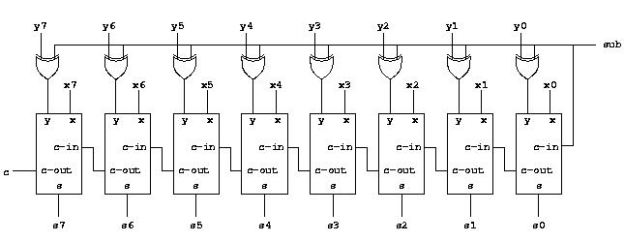
To demonstrate how this is done, consider that instead of computing the expression x - y, we can instead compute the expression x + -y. We learned how to negate a number by inverting all the bits and adding 1 in the section on binary arithmetic. As a result, the expression can be written as x + inv(y) + 1. All the inputs of the second operand must be inverted before they reach the adder, so how can we add the 1. That appears to necessitate the use of a separate adder for that purpose. We can take advantage of an unused carry-in signal to position 0 that we have. Giving this input a 1 adds one to the final output. The following is the entire circuit with addition and subtraction:
Multiplication and division in binary
Binary addition is more difficult than binary multiplication. We can't find a suitable iterative combinatorial circuit, so we'll have to utilise even more powerful artillery. A sequential circuit will be used to solve the problem, with one addition computed for each clock pulse. We'll go over this in more detail in a subsequent section because it requires mechanisms that we haven't yet covered.
3.5.4 Binary Arithmetic Circuits
The Half Adder
Combinal logic circuits perform binary arithmetic, the simplest of which is the half adder, as shown in Fig. 4.1.1. In its most basic form, this circuit consists of two gates: an XOR gate and a logic 1 output whenever A is 1 and B is 0, or when B is 1 and A is 0. When both A and B are 1, the AND gate produces a logic 1 at the carry output. Table 4.1.1 shows the half adder truth table, which describes the result of binary addition.
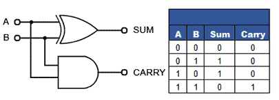
Fig: The Half Adder
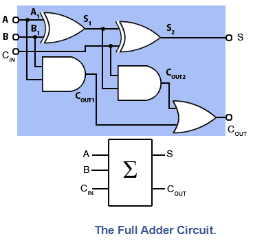
Fig: The Full Adder Circuit
1 plus 0 = 12 (110)
And
1 plus 1 = 102 (210)
The half adder is fine for adding two 1-bit numbers together, but for binary numbers containing several bits, a carry may be produced at some time (as a result of adding 1 and 1) that must be added to the next column. Because the half adder only has two inputs, it can't add in a carry bit from a previous column, hence it's only good for 1-bit adds.
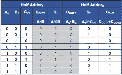
The Full Adder
The Full Adder, illustrated in Fig. 4.1.2 (blue backdrop) with its simplified block diagram symbol, is used when two or more bits need to be added. This circuit consists of two half adders, with the first half adder's total of A and B serving as input A to the second half adder, which creates a sum of the first half adder sum (S1) plus any "carry in" from the CIN terminal. The two half adders' carries are then 'ORed' together to form a single COUT. Output. Table 4.1.2 shows the truth table for the circuit.
Parallel Adders
Even though a full adder only adds two single bit binary integers, it can be paired with other full adders to create parallel adders that add two multibit integers. To add multibit binary values, parallel adders can be created in a variety of ways, with each bit of the parallel adder employing a single full adder circuit. Because drawing parallel adder circuits with all of the individual gates would be extremely complicated, it is usual to replace the full adder schematic diagram with a simplified block diagram version.
Bit Parallel Adder
Because any carry appearing at the carry in input (CIN) or produced when adding any of the 4-bit inputs ‘ripples' throughout the adder stages until a final carry out emerges at the carry out output (COUT) of the final full adder for bit A3+B3, Fig 4.1.3 is also known as a ‘Ripple Carry Adder.'
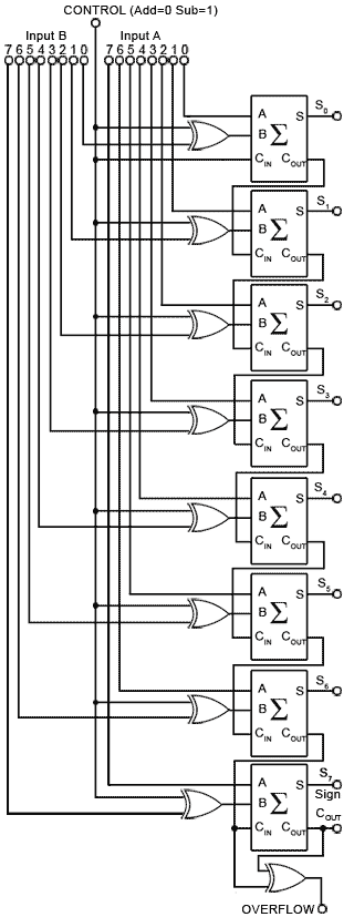
Fig. 8−Bit Twos Complement Adder/Subtractor.
8 Bit Twos Complement Adder/Subtractor
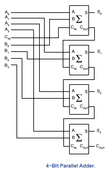
Fig: 4-Bit Parallel Adder
8 Bit Twos Complement Adder/Subtractor
However, in order to perform arithmetic, you must also be able to subtract. Figure 4.1.4 depicts a further evolution of the parallel adder. This is a parallel 8-bit adder/subtractor. This circuit adds in the same way as the adder in Fig. 4.1.3, but subtracts using the twos complement method described in Module 1.5 of Digital Electronics (Ones and Twos Complement).
When subtraction is needed, the control input is set to logic 1, causing the bit at either of the B inputs to be complemented by an XOR gate before being supplied to the complete adder circuit's input B.
In an 8-bit adder/subtractor, twos complement subtraction necessitates that the 8-bit value at input B be complemented (inverted) and 1 added before being added to the 8-bit number at input A. The result will be an 8-bit number in twos complement format, with the lower 7 bits (bits 0 to 6) representing the value and the most significant bit representing the sign (bit 7). To be included in the addition, the logic 1 on the control input is also sent to the first carry input of the adder, which for subtraction is:
Input A + Input B + 1
(Here + signifies addition rather than OR)
Alternatively, if addition of A and B is required, then the control input is at logic 0 and number B is fed to the adder without complementing.
Adder/Subtractor Control
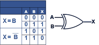
Fig. XOR Gate Used as a Data Selector.
The truth table for an XOR gate, illustrated in Table 4.1.3, shows how an XOR gate is used to convert the adder into a subtractor by inverting the B inputs (in Fig. 4.1.5). If the XOR gate's input A (used as the CONTROL input) is at logic 0, the XOR gate selects input B; however, if input A is at logic 1, the XOR gate selects the inverse of input B. (i.e.B).
Twos Complement Overflow
Figure 4.1.4 shows an 8-bit adder/subtractor that uses twos complement notation to add and subtract 8-bit binary values. The most significant bit (bit 7) is not used as part of the number's value in this system; instead, it is utilised to signify the number's sign (0 = positive, 1 = negative).
A certain number of bits can only process numbers up to a maximum value that can be held in its designated word length, regardless of the word size of a digital system (8 bits, 16 bits, 32 bits, etc.).
Adding two integers (with either positive or negative values) that are both within the system's limit can result in a result that is too large for the system's word length to hold during arithmetical operations.
When adding either positive or negative 7-bit values in a twos complement adder like the one shown in Fig. 4.1.4, the output could be larger than 7 bits can accommodate. As a result, the result will need to take up one more bit, causing the calculated value to ‘overflow' into bit eight, losing a significant portion (12810) of the value and changing the result's sign.
To tackle this problem, you must first notice that an overflow has happened, and then either use more circuits or, in computer, build a remedial process in software to address it.
Fortunately, there is a straightforward approach for detecting an overflow. The overflow detection system, as illustrated in Fig. 4.1.5, comprises of a single exclusive or (XOR) gate that receives its inputs from the bit 7 (sign bit) adder's carry in and carry out connections.
When the carry in (CIN) and carry out (COUT) bits of this adder are examined, it can be shown that if there has been an overflow, CIN and COUT will be different, but if there hasn't been an overflow, they will be same.
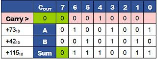
Adding Two Positive Numbers (Within a Range)
Table shows the effect of adding two positive values where the sum is within the range that can be held in 7 bits (≤12710). When two positive numbers are added together, the outcome is a proper positive result with no carry and no overflow.
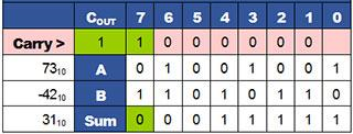
Twos Complement Subtraction
A twos complement subtraction is achieved by adding a negative number to a positive number, as shown in Table. The result is 3110 (within the range 0 to +12710), the sign bit is 0 indicating positive result, CIN and COUT are both 1, so no overflow is detected and the carry bit will be discarded.
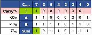
Adding Twos Complement Negative Numbers
Table shows the effect of adding two negative values where the sum is less than +12710 therefore a correct negative result of −7310 (in twos complement notation) has been obtained. CIN and COUT are both logic 1, thus no overflow will be detected. The carry will be ignored because only 8-bit computations are being examined.
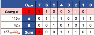
Out of Range Result Causes Overflow
When the sum of two positive values in Table. Is bigger than +12710, the sign bit is wrongly converted from 0 to 1, indicating a negative result. An overflow is detected because the ‘carry in' from bit 6 to bit 7 is 1 and the ‘carry out' from bit 7 to the Carry bit is 0. This indicates an incorrect solution.
Notice that the addition in Table is valid if the result of 100111012 is regarded an unsigned binary value (15710). However, because the calculation is done in twos complement notation, the result of 9910 must be rejected.

Out of Range Addition of Negative Values
Table indicates that if the sum of two negative numbers is bigger than 12810, it can result in a change in sign and an erroneous twos complement result. Adding 6310 and 7310 should have yielded a negative result of 13610, not +12010, in this situation. To verify this, the proper answer (though with the incorrect sign) might be achieved by complementing the answer and adding 1 to it, yielding an unsigned binary result of 100010002, which converts to 128 + 8 = 13610. Overflow issues can be fixed, but doing so would necessitate either extra electronics or a software response to the overflow signal.
Carry Look Ahead Adders
Because of the way the carry bit is propagated from one stage of the adder to the next, rippling through the chain of complete adders until the carry out is formed at the carry out pin of the final step, the adders described in this module are sometimes referred to as Ripple Carry Adders.
The amount of time it takes is proportional to the number of bits added. Although this may be a minor issue in tiny adders, the time delay before the final carry out is created becomes undesirable as the number of bits in the binary words to be added increases.
To address this issue, IC manufacturers offer a variety of ‘Carry Look Ahead Adders,' which produce both the addition and the carry out at the same time. Based on the state of the A and B inputs to that stage, as well as the logic state of the carry in bit to the first stage, the system employs complicated combinational logic to determine if a carry will be formed at each individual adder.
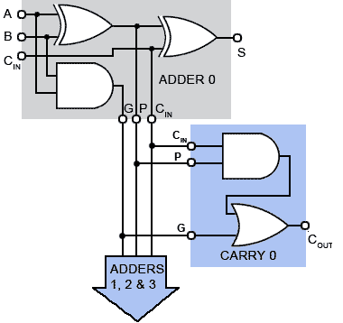
Figure: The Initial Stage of a Carry Adder, be on the lookout
In Fig, the full adder is split into a partial full adder (grey block), which has two extra outputs: a propagate (P) output that takes a logic 1 output anytime inputs A and B are 1,0 or 0,1 and a generate (G) output that will be logic 1 anytime the A and B inputs are at 1,1. It is feasible to decide on the logic state of the carry out based on a combination of the CIN state and the A and B states using this information.
The P input is ANDed with the CIN and ORed with the G input in the carry generator (blue block) to produce a carry out. The carry out is fed to the successive adders as usual, but the CIN P and G signals are fed in parallel to the other adder stages, allowing the state of the carry out for each adder stage to be determined from the shared CIN signal and the A and B states for the successive stages, depending on the input states at each stage, rather than waiting for the calculations to complete at all.
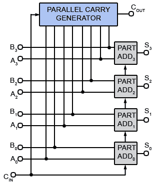
Fig. Carry Look Ahead Adder, Block Diagram
The carry out (COUT) is formed by the parallel carry generator from the A and B input signals and the CIN signal, rather than from the carry out of the final adder stage as in the ripple adders, as shown in a simplified block diagram.
Look ahead adders are useful in practical circuits because having an adder that generates part of its answer (the sum) at one time and another portion of its answer (the carry out) at a different time might cause timing problems in other portions of the circuit.
3.6.1 Addition and Subtraction using 2's complement
In our previous section, we learned how we could perform arithmetic operations such as addition and subtraction using 1's complement. We'll learn how to do these operations using 2's complement in this section.
Addition using 2's complement
When we add two binary numbers using 2's complement, there are three potential instances that can occur:
Case 1: Addition of the positive number with a negative number when the positive number has a greater magnitude.
Find the two's complement of the given negative number first. Add the specified positive number to the total. The number will be a positive number if we get the end-around carry 1, and the carry bit will be discarded, leaving the remaining bits as the final result.
Example: 1101 and -1001
1. To begin, determine the negative integer 1001's 2's complement. To find the 2's complement, turn all 0s to 1s and all 1s to 0s, or find the 1's complement of 1001. Add 1 to the LSB of the result 0110 to get the 1's complement of the number 1001. As a result, the 2's complement of 1001 is 0110+1=0. 112
2. Add the numerals 1101 and 0111 together; 1101+0111=1 0100
3. We get the end-around carry 1 by adding both values. The end-around carry is discarded. As a result, the sum of both numbers equals 0100.
Case 2: Adding of the positive value with a negative value when the negative number has a higher magnitude.
To begin, add a positive value to the negative number's 2's complement value. There is no end-around carry here. To get the final result, we take the 2's complement of the result.
1. Find the negative number 1110's 2's complement first. Add 1 to the LSB of the 1's complement value 0001 to discover 2's complement. 0001+1=0010
2. Add the numbers 1101 and 0010 together.
1101 plus 0010 equals 1111.
3. Find the 2's complement of the final result, which is 1110. As a result, the 2's complement of the result 1110 is 0001, and we can tell it's a negative integer by adding a minus sign before it.
Case 3: Addition of two negative numbers
In this example, we'll find the 2's complement of both negative values, then add the two complement numbers together. In this scenario, we'll always obtain the end-around carry, which will be added to the LSB, and we'll take the 2's complement of the result instead of the final result.
Example: -1101 and -1110 in five-bit register
1. First, determine the negative numbers 01101 and 01110's 2's complement. So, to determine 2's complement, we add 1 to the LSB of these integers' 1's complement. 01110 has a 2's complement of 10010, and 01101 has a 2's complement of 10011.
2. We multiply both complement numbers, 10001 and 10010, to get 1 00101; 10010+10011= 1 00101
3. We get the end-around carry 1 by adding both values. The carry is removed, and the final result is the 2.s complement of 00101. As a result, the 2's complement of 00101 is 11011, and we append a negative sign before the number to indicate that it is a negative number.
3.6.2 Addition with the 2's complement
To subtract two binary numbers using 2's complement, follow these steps.
o Find the 2's complement of the subtrahend in the first step.
o Take the complement number and multiply it by the minuend.
o If we receive the carry by adding both integers, we ignore it and the result is positive; otherwise, we take the result's 2's complement, which is negative.
Example 1: 10101 - 00111
Subtrahend 00111 is 2's complement, which is 11001. Now add them up. As a result, 10101+11001 Equals 1 01110.
We receive the carry bit 1 in the above result. As a result, we discard the carry bit and are left with the final result, which is a positive value.
Example 2: 10101 - 10111
We get 01001 by taking the 2's complement of subtrahend 10111. Now we add the two numbers together. As a result, 10101+01001 Equals 11110.
We didn't obtain the carry bit in the above result. Calculate the result's 2's complement, which is 00010. It's the ultimate solution and a negative number.
3.6.3 Subtraction of two numbers using 2’s Complement
Given two numbers a and b. The task is to subtract b from a by using 2’s Complement method.
Note: Negative numbers represented as 2’s Complement of Positive Numbers.
For example, -5 can be represented in binary form as 2’s Compliment of 5. Look at the image below:
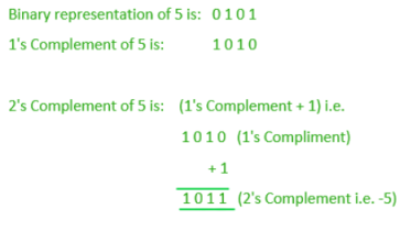
Examples:
Input: a = 2, b = 3
Output: -1
Input: a = 9, b = 7
Output: 2
To take away b from a. (a-b) = a + (a-b) = a + (a-b) = a + (a-b) = a + (a-b) = a + (a-b (-b)
(2's complement of b) can now be expressed as (-b). As a result, the above expression can now be written as:
a + (2's complement of b) Equals (a - b)
As a result, the problem now boils down to "Add a to the 2's complement of b." For the first example, where a = 2 and b = 3, the figure below depicts the above method of subtraction.
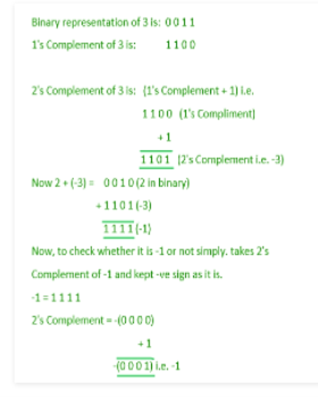
Below is the implementation of the above method:
- C++
- Java
- Python3
- C#
- PHP
- Javascript
#include <bits/stdc++.h> Using namespace std; // function to subtract two values // using 2's complement method Int Subtract(int a, int b) { Int c; // ~b is the 1's Complement of b // adding 1 to it make it 2's Complement c = a + (~b + 1);
Return c; }
// Driver code Int main() { Int a = 2, b = 3;
Cout << Subtract(a, b)<<endl;
a = 9; b = 7; Cout << Subtract(a, b);
Return 0; } |
Output
-1
2
Method 2: Basic Approach or Brute Force Approach
Subtraction of two binary values using the 2's Compliment approach.
Step 1: Determine the subtrahend's 2's complement.
Step 2: Add the initial number and the subtrahend's 2's complement.
Step 3: If the carry is created, throw it out. If there is no carry, take the result's 2's complement.
The implementation of the above strategy is shown below.
- C++
- Java
- C#
- Javascript
//C++ code for above approach
#include<iostream>
#include<bits/stdc++.h>
Using namespace std;
// Program to substract
Void Subtract(int n, int a[],
Int b[])
{
// 1's Complement
For(int i = 0; i < n; i++)
{
//Replace 1 by 0
If(b[i] == 1)
{
b[i] = 0;
}
//Replace 0 by 1
Else
{
b[i] = 1;
}
}
//Add 1 at end to get 2's Compliment
For(int i = n - 1; i >= 0; i--)
{
If(b[i] == 0)
{
b[i] = 1;
Break;
}
Else
{
b[i] = 0;
}
}
// Represents carry
Int t = 0;
For(int i = n - 1; i >= 0; i--)
{
// Add a, b and carry
a[i] = a[i] + b[i] + t;
// If a[i] is 2
If(a[i] == 2)
{
a[i] = 0;
t = 1;
}
// If a[i] is 3
Else if(a[i] == 3)
{
a[i] = 1;
t = 1;
}
Else
t = 0;
}
Cout << endl;
// If carry is generated
// discard the carry
If(t==1)
{
// print the result
For(int i = 0; i < n; i++)
{
// Print the result
Cout<<a[i];
}
}
// if carry is not generated
Else
{
// Calculate 2's Compliment
// of the obtained result
For(int i = 0; i < n; i++)
{
If(a[i] == 1)
a[i] = 0;
Else
a[i] = 1;
}
For(int i = n - 1; i >= 0; i--)
{
If(a[i] == 0)
{
a[i] = 1;
Break;
}
Else
a[i] = 0;
}
// Add -ve sign to represnt
Cout << "-";
// -ve result
// Print the resultant array
For(int i = 0; i < n; i++)
{
Cout << a[i];
}
}
}
// Driver Code
Int main()
{
Int n;
n = 5;
Int a[] = {1, 0, 1, 0, 1},
b[] = {1, 1, 0, 1, 0};
Subtract(n,a,b);
Return 0;
}
Output
-00101
3.7.1 Explanation of Half Adder and Full Adder with Truth Table
Different logic gates are used to create encoder, multiplexer, decoder, and de-multiplexer in combinational circuits. These circuits have some characteristics, such as the fact that the output of this circuit is primarily determined by the levels present at the input terminals at any given time. There is no memory in this circuit. The previous state of the input has no bearing on the current state of the circuit. In a combinational circuit, there are ‘n' number of inputs and ‘m' number of outputs. Half and full adders, subtractors, encoders, decoders, multiplexers, and demultiplexers are examples of combinational circuits. This page provides an overview of the half adder and full adder algorithms, as well as how they interact with truth tables.
What is an Adder?
In electronics, an adder is a digital logic circuit that is commonly used to add numbers. Adders are used in many computers and other types of processors to calculate addresses and associated actions, as well as construct table indices in the ALU and other portions of the CPU. Many numerical representations, such as excess-3 or binary coded decimal, can be formed with these. Adders are divided into two categories: half adders and full adders.
What is Half Adder and Full Adder Circuit?
A and B are the two inputs of the half adder circuit, which add two input digits and output a carry and a sum. The full adder circuit contains three inputs: A, B, and C, which add three values and provide a carry and sum. This article provides thorough information in tabular form as well as circuit diagrams on what a half adder and full adder are used for. The primary and most important function of adders has previously been discussed. The half adder and full adder theories are explained below.

Fig: Basic half adder and full adder
Half Adder
So, in the case of a half adder, it adds two binary digits, where the input bits are referred to as augend and addend, and the result is two outputs, one of which is the sum and the other of which is the carry. XOR is used to both inputs to execute the sum operation, while AND gate is applied to both inputs to provide carry.
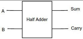
The full adder circuit, on the other hand, adds three one-bit values, with two of the three bits referred to as operands and the other as bit brought in. Output carry and sum are terms used to describe the 2-bit output that is produced.
With the help of logic gates and a half adder, you can design simple addition.
Let's look at an example of how to add two single bits.
The truth table for a 2-bit half adder is as follows:
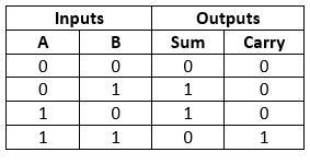
0+0 = 0
0+1 = 1
1+0 = 1
1+1 = 10
These are the least possible single-bit combinations. But the result for 1+1 is 10, the sum result must be re-written as a 2-bit output. Thus, the equations can be written as
0+0 = 00
0+1 = 01
1+0 = 01
1+1 = 10
The output ‘1’of ‘10’ is carry-out. ‘SUM’ is the normal output and ‘CARRY’ is the carry-out.
It has now been established that a 1-bit adder can be simply created using an XOR Gate for the ‘SUM' output and an AND Gate for the ‘Carry' output.
When we need to add two 8-bit bytes together, for example, we can use a full-adder logic circuit. When you need to add one binary digit quantities, the half-adder comes in handy.
Making a truth table and reducing it is one technique to construct two-binary digit adders. The half adder addition action is repeated twice to create a three binary digit adder. Similarly, if you want to construct a four-digit adder, you must repeat the process once more. With this hypothesis, it was evident that implementation would be straightforward, but development would take time.
The exclusive OR function is used in the simplest expression:
Sum= A XOR B
Carry = A AND B
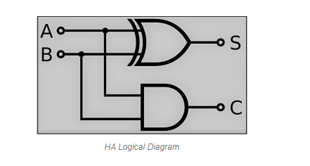
And an equivalent expression in terms of the basic AND, OR, and NOT is:
SUM=A.B+A.B’
VHDL Code For Half Adder
Entity ha is
Port (a: in STD_LOGIC;
b : in STD_LOGIC;
Sha : out STD_LOGIC;
Cha : out STD_LOGIC);
End ha;
Architecture Behavioral of the above circuit is
Begin
Sha <= a xor b;
Cha <= a and b;
End Behavioral
Half Adder IC Number
Half adders can be implemented using high-speed CMOS digital logic integrated circuits such as the 74HCxx series, which includes the SN74HC08 (7408) and SN74HC86 (7408). (7486).
Half Adder Limitations
Because there is no range to include the carry bit utilising an earlier bit, these binary adders are referred to as Half Adders. As a result, this is a major drawback of HAs when employed as a binary adder, especially in real-time scenarios where multiple bits must be added. As a result, by using the complete adders, this limitation can be bypassed.
Full Adder
When compared to the half-adder, this adder is more complicated to construct.
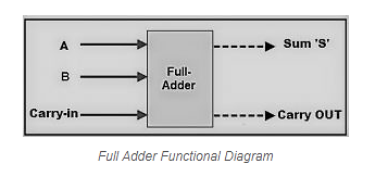
A half-adder differs from a full-adder in that the full-adder has three inputs and two outputs, whereas the half-adder has just two inputs and two outputs. The first two inputs are A and B, with the third being a C-IN input. When you construct full-adder logic, you thread eight of them together to make a byte-wide adder, and the carry bit is cascaded from one adder to the next.
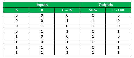
The carry output is labelled as C-OUT, and the normal output is denoted as S, which stands for ‘SUM.'
The implementation of a complete adder circuit can be simply understood using the above complete adder truth-table. The SUM ‘S' is made up of two parts:
1. XOR the supplied inputs 'A' and 'B'
2. The A XOR B result is then XORed with the C-IN result.
This produces SUM, and C-OUT is true only if two of the three inputs are HIGH, in which case C-OUT is HIGH. With the help of two half adder circuits, we can create a full adder circuit. To get the final S output, the half adder will first add A and B to form a partial Sum, and then a second-half adder logic will add C-IN to the Sum created by the first half adder.
There will be an output carry if any of the half adder logic causes a carry. As a result, C-OUT will be an OR function of the Carry outputs from the half-adder. Take a look at how the whole adder circuit is implemented in the diagram below.
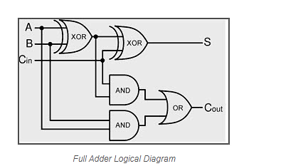
With the aforementioned full adder logic, larger logic diagrams can be implemented. The operation is usually represented by a simpler symbol. A simplified schematic illustration of a one-bit complete adder is shown below.
We can combine two bits with this symbol, taking a carry from the next lower order of magnitude and passing it to the next higher order of magnitude. For a multi-bit operation in a computer, each bit must be represented by a whole adder and added at the same time. To add two 8-bit values, you'll need eight full adders, which can be made by cascading two 4-bit blocks together.
Half Adder and Full Adder using K-Map
The Karnaugh map approach can also be used to obtain the sum and carry outputs for a half adder (K-map). K-map can be used to obtain the half adder and full adder boolean expressions. As a result, the K-map for these adders will be detailed further down.
The K-map with half adders is
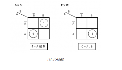
The complete K-Map adder is available.
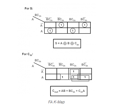
SUM and CARRY LOGICAL EXPRESSION
Based on the inputs listed in the table, the logical expression of sum (S) can be established.
= A’B’Cin + A’ B CCin’ + A B’Cin’+ AB Cin
= Cin (A’B’+ AB) + Cin’ (A’B +A B’)
= Cin EX-OR (A EX-OR B)
= (1,2,4,7)
Based on the inputs shown in the table, the logical expression of the carry (Cout) can be calculated.
= A’B Cin + AB’Cin + AB Cin’ + ABCin
= AB + BCin + ACin
= (3, 5, 6, 7)
The results can be acquired using the above-mentioned truth tables, and the approach is as follows:
A combinational circuit combines the circuit's several gates, which can include encoders, decoders, multiplexers, and demultiplexers. Combinational circuits have the following features.
1. At any given time, the output is solely determined by the levels present at the input terminals.
2. It has no memory requirements. The prior state of the input has no bearing on the circuit's current state.
3. It can have an infinite number of inputs and m outputs.
3.7.2 VHDL Coding
VHDL coding for full adder include the following.
Entity full_add is
Port ( a : in STD_LOGIC;
b : in STD_LOGIC;
Cin : in STD_LOGIC;
Sum : out STD_LOGIC;
Cout : out STD_LOGIC);
End full_add;
Architecture Behavioral of full_add is
Component ha is
Port ( a : in STD_LOGIC;
b : in STD_LOGIC;
Sha : out STD_LOGIC;
Cha : out STD_LOGIC);
End component;
Signal s_s,c1,c2: STD_LOGIC ;
Begin
HA1:ha port map(a,b,s_s,c1);
HA2:ha port map (s_s,cin,sum,c2);
Cout<=c1 or c2 ;
End Behavioral;
The distinction between a half adder and a full adder is that a half adder produces results, whereas a full adder employs a half adder to generate a different result. While the Full-Adder is made up of two Half-Adders, it is the real block that we employ to build arithmetic circuits.
Carry Lookahead Adders
The bits required for addition are readily available under the concept of ripple carry adder circuits. Every adder section, on the other hand, must wait for carry from the preceding adder block to arrive. As a result, SUM and CARRY take longer to produce since each section of the circuit must wait for input.
To produce output for the nth block, for example, it must first take input from the (n-1)th block. Propagation delay is the word used to describe this delay.
A carry-lookahead adder was introduced to address the latency in ripple carries adders. The propagation latency can be reduced here by employing complex hardware. A carry-lookahead adder using full adders is shown in the diagram below.
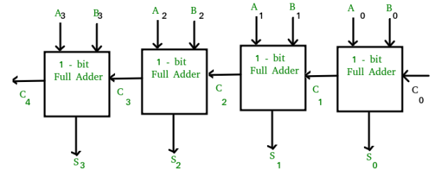
The truth table and corresponding output equations are
A | B | C | C+1 | Condition |
0 | 0 | 0 | 0 | No Carry Generate |
0 | 0 | 1 | 0 | |
0 | 1 | 0 | 0 | |
0 | 1 | 1 | 1 | No Carry Propagate |
1 | 0 | 0 | 0 | |
1 | 0 | 1 | 1 | |
1 | 1 | 0 | 1 | Carry Generate |
1 | 1 | 1 | 1 |
Pi = Ai XOR Bi is the carry propagates equation, and Gi = Ai*Bi is the carry generate equation. The sum and carry equations can be expressed as with these equations.
SUM = Pi XOR Ci
Ci+1 = Gi + Pi*Ci
Gi delivers carry only when both the inputs Ai and Bi are 1 without considering the input carry. Pi is related to the carry propagation from Ci to Ci+1.
Difference between Half Adder and Full Adder
The difference between the half adder and full adder table is shown below.
Half Adder | Full Adder |
The Half Adder (HA) is a combinational logic circuit that is used to add two one-bit numbers together. | The Full Adder (FA) is a combinational circuit that adds three one-bit digits together. |
In HA, once the carry from the previous addition is generated, it cannot be added to the following step. | Once the carry has been generated from the previous addition, it can be applied to the following step in FA. |
The half adder has two logic gates, the AND and EX-OR gates. | Two EX-OR gates, two OR gates, and two AND gates make up the whole adder. |
The half adder takes two input bits, A and B. | The complete adder has three input bits, A, B, and C-in. |
Half adder sum and carry equation is S = a⊕b ; C = a*b | Full adder logic expression is S = a ⊕ b⊕Cin; Cout = (a*b) + (Cin*(a⊕b)). |
HA is found in computers, calculators, and digital measurement instruments, among other things. | Digital processors, multiple bit addition, and other applications use FA. |
The key differences between the half adder and full adder are discussed below.
1. A half adder adds two binary inputs to generate sum and carry, whereas a full adder adds three binary inputs to generate sum and carry. The hardware architecture of a half adder and a full adder are not the same.
2. The fundamental feature that distinguishes HA from FA is that in HA, the last addition carry is not treated as an input. However, an FA looks for a specific input column, such as Cin, to evaluate the carry bit of the previous addition.
3. Based on the components used in the circuit's construction, the two adders will indicate a difference. Half adders (HAs) use a combination of two logic gates, such as AND and EX-OR, whereas the FA uses a combination of three AND, two XOR, and one OR gate.
4. In general, HAs work with two 1-bit inputs, whereas FAs work with three 1-bit inputs. A half adder is used to evaluate addition in many electronic devices, whereas a full adder is used in digital processors to add a long bit.
5. The HA and FA are also combinational digital circuits, which means they don't use any memory elements like sequential circuits. These circuits are required for arithmetic operations in order to add binary numbers.
Full Adder Implementation using Half Adders
A FA can be implemented with two logically connected half adders. The connecting of an FA utilising two half adders is illustrated in the block diagram below.
The sum and carry equations from previous calculations are
S = A‘ B’ Cin + A’ BC’ in + ABCin
Cout = AB + ACin + BCin
The sum equation can be written as.
Cin (A’B ‘+ AB) + C ‘in (A‘B + A B’)
So, Sum = Cin EX-OR (A EX-OR B)
Cin (A EX-OR B) + C’in (A EX-OR B)
= Cin EX-OR (A EX-OR B)
Cout can be written like the following.
COUT = AB + ACin + BCin.
COUT = AB + ACin+ BCin (A + ̅A)
= ABCin + AB + ACin + A’ B Cin
= AB (1 + Cin) + ACin + A’ B Cin
= A B + ACin + A’ B Cin
= AB + ACin (B + B’ ) + A’ B Cin
= ABCin + AB + A’B Cin+ A’ B Cin
= AB (Cin + 1) + A B Cin + A’ B Cin
= AB + AB’ Cin + A’ B Cin
= AB + Cin ( AB’ + A’B )
Therefore, COUT = AB + Cin (A EX-OR B)
Depending on the above two sums & carry equations, the FA circuit can be implemented with the help of two HAs & an OR gate. A complete adder with two half adders is shown in the circuit diagram above.
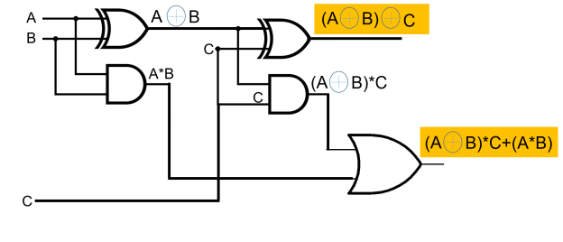
Full Adder Design with using NAND Gates
A NAND gate is a type of universal gate that can be used to perform any logic design. Below is a diagram of the FA circuit with NAND gates.
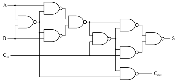
FA is a simple one-bit adder, and if we want to add n bits, we'll need to use n number of one-bit FAs in the cascade connection structure.
Advantages
The following are some of the benefits of using a half adder or a full adder.
1. A half adder's primary function is to add two single-bit values.
2. Full adders are capable of adding a carry bit, which is the result of the previous addition.
3. Critical circuits such as adder, multiplexer, and many more can be built with a full adder.
4. The entire adder circuits use very little power.
5. The advantages of a full adder over a half adder are that a full adder is used to overcome the disadvantages of a half adder, which is that the half adder is primarily used to add two 1-bit values. Because half adders don't add the carry bit, a full adder is used to compensate. Three bits can be added in a full adder, which yields two outputs.
6. Adders are straightforward to design and are a fundamental building block for understanding one-bit addition.
7. By adding an inverter, this adder can be transformed to a half subtractor.
8. High output can be produced by utilising a full adder.
9. Quickness
10. The ability to offer voltage scaling is really powerful.
Disadvantages
The disadvantages of half adder and full adder include the following.
1. Half adders cannot be used before carrying, hence they are ineffective for cascading multi-bit additions.
2. To compensate for this flaw, FA must add three 1 bits.
3. When the FA is utilised as part of a chain, such as a RA (Ripple Adder), the output drive capability might be reduced.
4. Useful applications
5. Half adder and full adder uses include the following.
6. Because the computer employs an adder, the binary bits addition can be done by a half adder utilising ALU.
7. A full adder circuit can be designed using a half adder combination.
8. Half adders are employed in calculators as well as to measure addresses and tables.
9. In digital circuits, these circuits are employed to address various purposes. It will play an important role in digital electronics in the future.
In many big circuits, such as the Ripple Carry Adder, an FA circuit is employed as an element. This adder simultaneously adds the number of bits.
11. In the Arithmetic Logic Unit, FAs are used (ALU)
12. FAs are employed in graphics applications such as GPUs (Graphics Processing Unit)
13. These are utilised to perform Carryout Multiplication in the multiplication circuit.
14. The Arithmetic Logic Unit uses Full Adders to construct the memory address and develop the programme counterpoint toward subsequent instructions in a computer.
15. As a result, whenever two binary numbers are added, the digits with the least bits are added first. Because the simplest n/w that permits adding two 1-bit values is a half adder, this procedure can be done with one. The binary digits are the adder's inputs, while the sum (S) and carry (C) are the adder's outputs (C).
The HA network is only used to connect the least digits when the number of digits is included, because the HA cannot add the carry number from the previous class. The base of all digital arithmetic devices can be characterised as a full adder. This is how you add three one-digit integers together. The inputs to this adder are A, B, and Cin, while the outputs are Sum and Cout.
3.7.3 Half Adder and Full Adder Circuit
A device that can add two binary digits is known as an adder. It's a type of digital circuit that conducts two-number addition operations. It is primarily intended for binary number addition, but it may also be used in other applications such as binary code decimal, address decoding, table index computation, and so on.
Adders come in two varieties. Half Adder and Full Adder are two types of adders. Below is a full explanation of the two sorts of adders.
Half Adder
In a Half Adder, there are two inputs and two outputs. A and B are the inputs, whereas Sum (S) and Carry are the outputs (C). The inputs A and B are X-ORed to produce the Sum. Carry is the product of the two inputs A and B. With the use of a half adder, one can create a circuit capable of doing simple addition using logic gates.
Let's look at the addition of single bits first.
0 + 0 = 0
0 + 1 = 1
1 + 0 = 1
1 + 1 = 10
These are the fewest single-bit combinations conceivable. However, the result for 1 + 1 = 10 is different. With the use of an EX-OR gate, this difficulty can be solved. The totals can be rewritten as a 2-bit output.
As a result, the preceding combination can be written as:
0 + 0 = 00
0 + 1 = 01
1 + 0 = 01
1 + 1 = 10
The carry-out is the output "1" of "10" in this case. The normal output is SUM, while the carry-out is CARRY.
The truth table of the half adder is shown below:
Inputs | Outputs | ||
A | B | Sum | Carry |
0 | 0 | 0 | 0 |
0 | 1 | 1 | 0 |
1 | 0 | 1 | 0 |
1 | 1 | 0 | 1 |
The Half Adder Circuit is shown below:
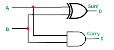
The fundamental drawback of this circuit is that it can only combine two inputs, and any carry is ignored. As a result, the procedure is unfinished.
Full Adder was created to help you solve this challenge. It's possible that you'll have to add two 8-bit bytes together while conducting sophisticated addition. Full Adder can be used to do this.
Full Adder
It's a little more difficult to implement a complete adder than a half adder. The main difference between a half adder and a full adder is that the full-adder has three inputs and two outputs. A and B are the two inputs, with CIN serving as a carry input. The regular output is labelled S, whereas the carry output is labelled COUT.
The truth table of the Full Adder Circuit is shown below.
Inputs | Outputs | |||
A | B | CIN | COUT | S |
0 | 0 | 0 | 0 | 0 |
0 | 0 | 1 | 0 | 1 |
0 | 1 | 0 | 0 | 1 |
0 | 1 | 1 | 1 | 0 |
1 | 0 | 0 | 0 | 1 |
1 | 0 | 1 | 1 | 0 |
1 | 1 | 0 | 1 | 0 |
1 | 1 | 1 | 1 | 1 |
The output S is an EX-OR between the input A and the SUM output B from the half-adder. Only one of the three inputs must be HIGH or at logic 1 for the COUT to be true.
With the help of two half adder circuits, a full adder circuit may be created. To obtain a partial total, the first half adder circuit will be utilised to add A and B. CIN can be added to the sum produced by the first half adder circuit using the second half adder logic. Finally, we get the output S.
There will be an output carry if any of the half adder logic causes a carry. As a result, COUT will be an OR function of the CARRY outputs from the half adder.
The Full adder circuit diagram is shown below:
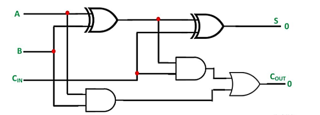

One can add two bits together with this type of symbol by taking a carry from the next lower order of magnitude and sending a carry to the next higher level of magnitude.
For a multi-bit operation in a computer, each bit must be represented by a whole adder and added at the same time. To add two 8-bit numbers, you'll need eight full addresses, which can be made by cascading two 4-bit blocks.
The following is the result of adding the four-bit number:

The Full Adder is used to perform sophisticated additions, such as combining two 8-bit values.
3.8.1 Full Subtractor
Only two numbers are subtracted with the Half Subtractor. A complete subtractor was created to solve this problem. To subtract three 1-bit values A, B, and C, which are minuend, subtrahend, and borrow, respectively, the full subtractor is employed. The full subtractor has three states of input and two states of output, diff and borrow.
Block diagram

Truth Table

The input variables in the above table are o'A' and'B'. The two significant bits that will be removed are represented by these variables.
o The third input, 'Borrow in,' stands for borrow.
o The output variables 'Diff' and 'Borrow' provide the output values.
o The eight rows under the input variable represent all conceivable 0 and 1 combinations in these variables.
With the help of K-map, you may get the SOP form like follows:
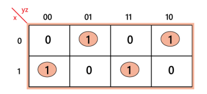
Diff=xy' z'+x' y' z+xyz+x'yz'
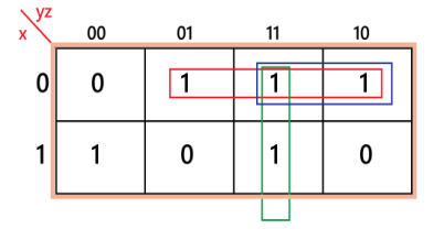
Borrow=x' z+x' y+yz
Construction of Full Subtractor Circuit:

The Full subtractor circuit is built as shown in the block diagram above. The OR gate is used to join two half adder circuits in the circuit shown above. A and B are two single-bit binary inputs in the first half subtractor. The half subtractor, as we all know, has two outputs: 'Diff' and 'Borrow.' The first subtractor's 'Diff' output will be the second half subtractor's first input, and the first subtractor's 'Borrow' output will be the second half subtractor's second input. 'Diff' and 'Borrow' will be provided by the second half subtractor once more. The 'Diff' bit is the result of the Full subtractor circuit. We feed the 'Borrow' of the first and second subtractors through the OR gate to determine the final output of the 'Borrow'. The final carry 'Borrow' of the entire subtractor circuit will be the result of the OR gate.
The final 'Borrow' bit represents the MSB.
The whole subtractor logic circuit can be built using an OR gate and the AND, XOR, and NOT gates.
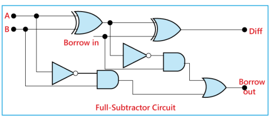
The whole subtractor's actual logic circuit is depicted in the diagram above. A Boolean expression can also be used to represent the complete subtractor circuit.
Diff: o Combine inputs A and B using the XOR method.
o Using 'Borrow,' perform an XOR operation on the result. As a result, the difference is (A XOR B) XOR 'Borrowin,' which can also be written as:
'Borrowin' (A) 'Borrowin' (B) 'Borrowin' (A) 'Borrowin'
Borrow:
o Combine the inverted inputs A and B using the 'AND' procedure.
o Combine inputs A and B using the 'XOR' function.
o Combine the two outputs from the previous two steps using the 'OR' operator. As a result, the 'Borrow' can be written as:
(A B) + A'.B'
3.8.2 Half Subtractor
The half-subtractor is a combinational circuit for doing two-bit subtraction. A (minuend) and B (subtrahend) are the two inputs, while Difference and Borrow are the two outputs. The truth table and logic symbol are provided below.
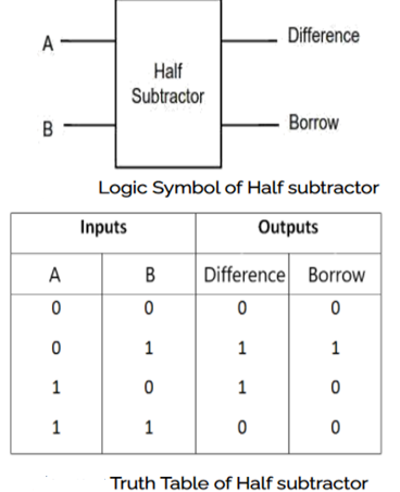
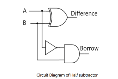
From the above truth table we can find the boolean expression.
Difference = A ⊕ B
Borrow = A' B
The half-subtractor circuit can be drawn from the equation as shown in figure 3.
3.8.3 Full Subtractor
A complete subtractor is a three-bit combinational circuit that conducts subtraction using the A (minuend), B (subtrahend), and Bin (borrow-in) bits. It takes three inputs: A (minuend), B (subtrahend), and a Bin (borrow bit), and outputs D (difference) and Bout (borrow bit) (borrow out). The truth table and logic symbol are provided below.
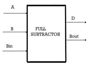
Fig: Logica symbol of full subtractor
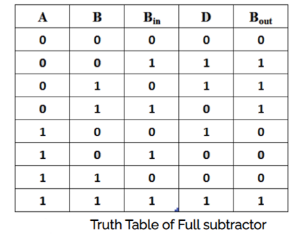
From the above truth table we can find the boolean expression.
D = A ⊕ B ⊕ Bin
Bout = A' Bin + A' B + B Bin
We may draw the Full-subtractor circuit from the equation, as shown in Figure 6.

3.8.4 What is a Half Subtractor: Circuit using Logic Gates
The “Logic Gates” are the most important idea in the field of electronics, on which every component is based. The notion of logic gates is used in a variety of applications, including integrated circuits, sensors, switches, microcontrollers and processors, encryption and decryption, and so on. Logic Gates have a wide range of applications in addition to these. Adder, Subtractor, Full Adder, Full Subtractor, Half Subtractor, and many other types of logic gates exist. As a result, this article covers the half subtractor circuit, half subtractor truth table, and associated topics.
Logical Circuit
The half subtractor logical circuit can be explained by using the logic gates:
- 1 XOR gate
- 1 NOT gate
- 1 AND gate
The representation is
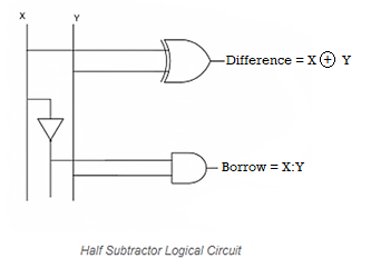
3.8.5 Half-Subtractor Block Diagram
The half subtractor's block diagram is depicted above. It takes two inputs and produces two outputs. A&B are used to represent the inputs, and Difference and Borrow are used to represent the outcomes.
EX-OR and NAND gates can be used to create the above circuit. The NAND gate can be constructed here by combining AND and NOT gates. To make half of a subtractor circuit, we'll need three logic gates: the EX-OR gate, NOT gate, and NAND gate.
When the AND and NOT gates are merged, a new gate called the NAND Gate is created. For the same inputs A&B, the Ex-OR gate output will be the Difference bit and the NAND gate output will be the Borrow bit.
AND-Gate
The AND-gate is one type of digital logic gate with multiple inputs and a single output and based on the inputs combinations it will perform the logical conjunction. When all of this gate's inputs are high, the output is high; otherwise, the output is low. The AND gate logic diagram with truth table is presented below.
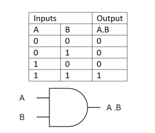
Fig. AND Gate and Truth Table
NOT Gate
The NOT-gate is one type of digital logic gate with a single input and based on the input the output will be reversed. When the NOT gate's input is high, for example, the output will be low. The NOT-gate logic diagram with the truth table is illustrated below. We can use this type of logic gate to perform NAND and NOR gates.
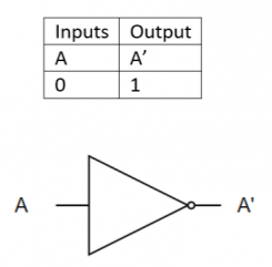
Fig. NOT Gate And Truth Table
Ex-OR Gate
Exclusive-OR, often known as EX-OR, is a form of digital logic gate with two inputs and a single output. The OR gate is required for this logic gate to function. If any of the EX-OR gate's inputs is high, the EX-OR gate's output will also be high. The EX-symbol OR's and truth table are displayed below.
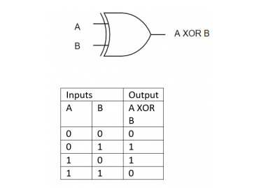
Fig. XOR Gate And Truth Table
Half Subtractor Circuit using Nand Gate
Logic gates such as the NAND gate and the Ex-OR gate can be used to build the subtractor. To create this half subtractor circuit, we must first understand the principles of difference and borrow.
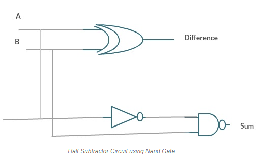
If we keep a close eye on this circuit, we can see that it performs a wide range of operations that are all connected to the EX-OR gate action. As a result, we can simply utilise the EX-OR gate to make a distinction. Similarly, the borrow induced by a half adder circuit can be easily achieved by combining logic gates such as AND-gate and NOT-gate.
This HS can also be constructed with NOR gates, with a total of 5 NOR gates required. The half subtractor circuit diagram utilising NOR gates is as follows:
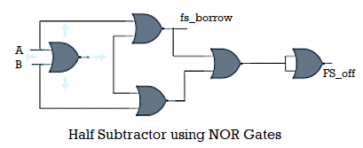
Truth Table
First Bit | Second Bit | Difference (EX-OR Out) | Borrow (NAND Out) |
0 | 0 | 0 | 0 |
1 | 0 | 1 | 0 |
0 | 1 | 1 | 1 |
1 | 1 | 0 | 0 |
VHDL and Testbench Code
The VHDL code for half subtractor is explained as follows:
Library IEEE;
Use IEEE.STD_LOGIC_1164.ALL;
Use IEEE.STD_LOGIC_ARITH.ALL;
Use IEEE.STD_LOGIC_UNSIGNED.ALL;
Entity Half_Sub1 is
Port ( a: in STD_LOGIC;
b: in STD_LOGIC;
HS_Diff: out STD_LOGIC;
HS_Borrow: out STD_LOGIC);
End Half_Sub1;
Architecture Behavioral of Half_Sub1 is
Begin
HS_Diff<=a xor b;
HS_Borrow<=(not a) and b;
The testbench code for HS is explained as below:
LIBRARY IEEE;
USE ieee.std_logic_1164.ALL;
ENTITY HS_tb IS
END HS_tb;
ARCHITECTURE HS_tb OF HS_tb IS
COMPONENT HS
PORT( a : IN std_logic;
b : IN std_logic;
HS_Diff : OUT std_logic;
HS_Borrow : OUT std_logic
);
END COMPONENT;
Signal a : std_logic := ‘0’;
Signal b : std_logic := ‘0’;
Signal HS_Diff : std_logic;
Signal HS_Borrow : std_logic;
BEGIN
Uut: HS PORT MAP (
a => a,
b => b,
HS_Diff => HS_Diff,
HS_borrow => HS_borrow
);
Stim_proc: process
Begin
a <= ‘0’;
b <= ‘0’;
Wait for 30 ns;
a <= ‘0’;
b <= ‘1’;
Wait for 30 ns;
a <= ‘1’;
b <= ‘0’;
Wait for 30 ns;
a <= ‘1’;
b <= ‘1’;
Wait;
End process;
END;
Full Subtractor Using Half Subtractor
A complete subtractor is a combinational device that uses two bits to do subtraction and is both minuend and subtrahend. The circuit uses the previous output as a borrow and has three inputs and two outputs. The minuend, subtrahend, and the input received from the preceding output, borrow, are the three inputs, while the difference and borrow are the two outputs.

Fig. Full Subtractor Logical Diagram
The truth table for full subtractor is
Inputs | Outputs | |||
X | Y | Yin | FS_Diff | FS_Borrow |
0 | 0 | 0 | 0 | 0 |
0 | 0 | 1 | 1 | 1 |
0 | 1 | 0 | 1 | 1 |
0 | 1 | 1 | 0 | 1 |
1 | 0 | 0 | 1 | 0 |
1 | 0 | 1 | 0 | 0 |
1 | 1 | 0 | 0 | 0 |
1 | 1 | 1 | 1 | 1 |
The logical diagram and circuits diagram for the implementation of a full subtractor utilising half subtractors is illustrated below, using the preceding truth table:
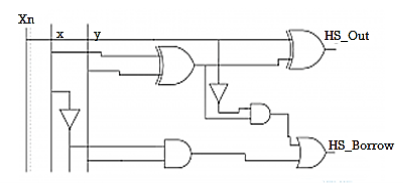
Fig. Full Subtractor Using HS
Advantages and Limitations of Half Subtractor
The advantages of half subtractor are:
1. This circuit's implementation and construction are simple and straightforward.
2. In digital signal processing, this circuit uses very little power.
3. Computational functions can be carried out at a faster rate.
4. The following are the constraints of this combinational circuit:
5. Despite the fact that the half subtractor has numerous applications in a variety of operations and functionality, it does have a few restrictions, which are as follows:
6. The half subtractor circuits do not accept "borrow-in" from earlier outputs, which is the circuit's most significant flaw.
7. Because many real-time applications require the subtraction of a large number of bits, half subtractors devices are incapable of doing so.
8. Half Subtractor Applications
The following are some of the half subtractor's applications.
1. A half subtractor is a device that is used to lower the strength of audio or radio signals.
2. It can be used to minimise sound distortion in amplifiers.
3. In the processor's ALU, a half subtractor is used.
4. It also calculates addresses and can be used to increase and decrease operators.
5. The least significant column numbers are subtracted with a half subtractor. It can be used for multi-digit numeric subtraction with the LSB.
6. Finally, we may conclude from the previous half subtractor theory that by employing this circuit, we may subtract one binary bit from another to produce outputs such as Difference and Borrow. Similarly, both NAND and NOR gates can be used to create a half subtractor.
3.9.1 4-bit binary Adder-Subtractor
A Binary Adder-Subtractor is a digital circuit that can do both addition and subtraction of binary numbers in the same circuit. The binary value of the control signal determines the operation to be executed. It's one of the ALU's components (Arithmetic Logic Unit).
Exor Gate, Binary Addition and Subtraction, and Full Adder are all prerequisites for this circuit.
Consider the following two 4-bit binary values as inputs to the Digital Circuit for digit operations: A and B.
A0 A1 A2 A3 A4 A5 A6 A7 A8 A9 A10 A11 A12 A
B0 B1 B2 B3 B4 B5 B6 B7 B8 B9 B10 B11 B12 B
Because we're working with 4-bit numbers, the circuit uses four complete adders. There is a control line K that has a binary value of either 0 or 1, indicating whether the operation is addition or subtraction.
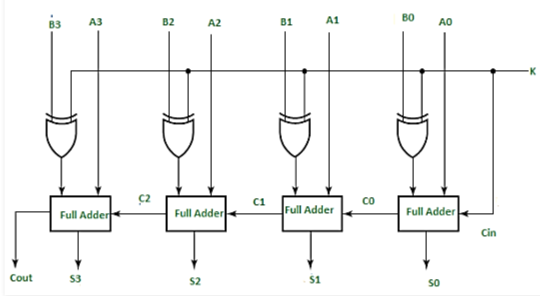
The first full adder, as shown in the diagram, has the control line as its direct input (input carry C0), and the input A0 (the least significant bit of A) is directly entered in the full adder. The exor of B0 and K (S in fig) is the third input. But don't mix it up with Sum-S). Sum/Difference (S0) and Carry are the two outputs produced (C1).
The output of B0(exor)K=B0′ if the value of K (Control line) is 1. (Complement B0). As a result, A+(B0′) would be the operation. A+B' is now the 2's complement subtraction for two numbers A and B. When K=1, the four-bit numbers are subtracted, implying that the operation is subtraction.
Likewise, If K is equal to 0, B0 (exor) K=B0. A+B is a straightforward binary addition procedure. When K=0, the operation performed on the four bit numbers appears to be addition.
The second complete adder receives C0 serially as one of its outputs.
The sum/difference S0 is recorded as the sum/least difference's significant bit. Direct inputs to the second, third, and fourth complete adders are A1, A2, and A3. The B1, B2, B3 EXORed with K to the second, third, and fourth full adders, respectively, is the third input. As one of the inputs, the carry C1, C2 is serially sent to the succeeding full adder. The entire carry to the sum/difference is C3. To form the result using S0, S1, S2, and S3 are recorded.
We use n complete adders to make an n-bit binary adder-subtractor.
Example:
Lets take two 3 bit numbers A=010 and B=011 and input them in the full adder with both values of control lines.
For K=0:
B0(exor)K=B0 and C0=K=0
Thus from first full adder
= A0+B0
= 0+1
= 1,
S0=1
C1=0
Similarly,
S1=0 with C2=1
S2=1 and C2=0
Thus,
A = 010 =2
B = 011 = 3
Sum = 0101 = 5
For K=1
B0(exor)K=B0' and C0=k=1
Thus
S0=1 and C1=0
Similarly
S1=1 and C2=0
S3=1 and c3=1
Thus,
A = 010 = 2
B = 011 = 3
Sum(Difference) = 1111 = -1
3.9.2 Binary Adder-Subtractor
Taking the 2's complements of addend bits and adding it to the augend bits is a simple way to do the Subtraction micro-operation.
By combining an exclusive-OR gate with each full adder, arithmetic micro-operations like addition and subtraction can be merged into a single circuit.
The following is a block schematic for a 4-bit adder-subtractor circuit:
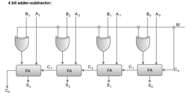
o The circuit acts as an adder when the mode input (M) is at a low logic, i.e. '0', and as a subtractor when the mode input (M) is at a high logic, i.e. '1'.
o Input M and one of the inputs B are sent to the exclusive-OR gate, which is connected in series.
o We have B 0 = B when M has a low logic.
The circuit receives the value of B, the input carry is 0, and it performs A plus B.
o We have B 1 = B' and C0 = 1 when M is at a high logic level.
Through the input carry, the B inputs are complemented, and a 1 is added. A plus the 2's complement of B is performed by the circuit.
3.9.3 Binary Adder/Subtractor (4 bit)
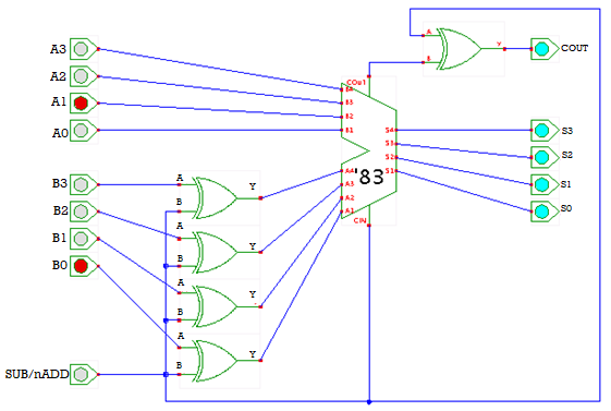
Circuit Description
Demonstration of a four-bit adder/subtractor. While designing a custom circuit for the subtraction operation is possible, it is far more typical to reuse an existing adder and replace the subtraction with a two-component addition.
This is demonstrated in the applet. To operate the Sub/nAdd switch, click the input switches or type the 's' bind key, and to control the A and B inputs, type '1'...'8'.
The XOR-gates operate as non-inverting buffers when the Sub/n Add input is low (0), and the carry-input to the adder is 0. As a result, the adder computes the following four-bit sum plus carry-out:
(A3,A2,A1,A0) + (Cout,S3,S2,S1,S0) (B3,B2,B1,B0)
The XOR-gates operate as inverting buffers when the Sub/nAdd input is high (1), and the carry-input to the adder is 1.
(A3,A2,A1,A0) = (Cout,S3,S2,S1,S0) (B3,B2,B1,B0)
3.10.1 Monostable Multivibrator using 555 Timer Circuit and Working
Multivibrators are widely used in pulse processing and generation systems. Multivibrators are electronic circuits used to build simple two-state systems such as timers, oscillators, and flip-flops. Two amplifying devices are cross-coupled via a resistor and a capacitor in these circuits. Astable multivibrators, monostable multivibrators, and bistable multivibrators are the three varieties of multivibrators based on the number of stable states. This article describes monostable multivibrators and monostable multivibrators using a 555 timer IC in detail.
Monostable Multivibrator
When an external trigger pulse is delivered, monostable multivibrators have only one stable state, which is utilised to generate a single o/p pulse of a defined width, either high or low. This trigger pulse initiates a timing cycle, causing the o/p to change state at the start of the timing cycle and then continue in the second state determined by the capacitor C and resistor R time constants until it returns to its original state. It will stay in this mode until it receives another i/p signal. Monostable multivibrators can generate a rectangular waveform that is substantially longer. When a trigger pulse is applied externally, the waveform's leading edge rises in response to the external trigger. The RC time constant of the feedback components utilised determines the trailing edge. This RC time constant can be changed over time to generate a series of pulses with a fixed time delay compared to the initial triggering pulse.
Fig: Monostable Multivibrators
Monostable Multivibrator using a 555 timer Circuit Diagram
The 555 Timer is an integrated circuit that can be used in a variety of applications, including timers, pulse generators, multivibrators, and oscillators. It is a highly stable controller that generates precise timing pulses. Astable, monostable, and bistable operating modes are available in these sorts of ICs. The delay is regulated by an external resistor and capacitor when the 555 timer IC is used in Mono-stable multivibrator mode. Two external resistors and one capacitor accurately control the frequency and duty cycle when it is employed in astable multivibrator operation.
Fig: 555 Timer IC
The word monostable refers to the fact that there is only one stable state in a monostable multivibrator employing a 555 timer circuit. "Quasi stable state" is the name given to the unstable condition. The charging time constant of the C network determines the period of stable state. The trigger switch was used to move o/p from a stable state to a quasi-stable condition. Below is a circuit diagram for a monostable multivibrator utilising a 555 timer. Using this circuit, we can quickly determine the pulse's duration.
Monostable multivibrator with 555 timer requires the following components: IC 555 timer, resistors, capacitors, and trigger switch.
Circuit Connections of Monostable Multivibrator with 555 Timer
Pin1 is linked to ground in the above circuit, while pin2 receives the trigger input. This i/p is held at +VCC when the o/p is inactive. A negative going pulse with a narrow width and amplitude bigger than +2/3 VCC is supplied to pin2 to transition the output from a stable to an unstable condition. To avoid inadvertent reset, the o/p is extracted from pin 3 and pin 4 is linked to +VCC. To reduce noise, Pin5 is linked to ground through a 0.01uF capacitor. Pins 6 and 7 are shorted, while pins 6 and 8 are linked via a resistor. Pin7 is connected to a discharge capacitor, whereas pin8 is connected to VCC.
Fig: Monostable Multivibrator using 555 Timer Circuit
Working of Monostable Multivibrator with 555 Timer Circuit
1. Until it receives a trigger, the output of the monostable multivibrator employing the 555 timer remains stable.
2. When both the transistor and the capacitor are shorted in a monostable 555 multivibrator, this is referred to be a stable state.
3. When the voltage on the 555 IC's second pin falls below a certain threshold, the o/p turns high. This high state is referred to as quasi-stable. When the circuit is turned on, it switches from a stable to a quasi-stable condition.
4. The discharge transistor is then turned off, and the capacitor begins to charge to VCC. The capacitor is charged through the resistor R1 with the time constant R1C1.
5. As a result, as the capacitor voltage rises and eventually exceeds 2/3 Vcc, the internal control flip flop changes, turning off the 555 timer IC.
6. As a result, the o/p returns to its stable condition after being in an unstable condition.
7. Finally, we can deduce that the o/p in the monostable multivibrator with 555 timer remains low until it receives a trigger i/p. In push-to-operate systems, this form of operation is used. When the input is activated, the o/p becomes high and then returns to its original condition.
555 timer Example
To create a time delay in a circuit, a Monostable multivibrator requires a 555 Timer IC. Calculate the value of the resistor necessary to provide a minimum o/p time delay of 500ms if a 10 uF timing capacitor is utilised.
R=1.1C/t
C=10uF, t=0. 5, t=0.
Fill in the blanks in the formula above.
R=0.1x10x10-2 R=0. 5/1.1x10x10-2 R=0. 5/1.1x10x10
=45.5kilo Ohms =45.5kilo Ohms =45.5kilo Oh
Applications of 555 timer in Monostable Mode
The 555 timer circuits are mostly used in monostable mode in many 555 timer-based projects.
Hidden Active Cell Phone Detector using a 555 timer
This project is designed to detect any activated mobile phone from a distance of about one-and-a-half feet to avoid the use of un-authorized cell phone in prohibited areas. The active mobile phone detector in this project is made with a 555 timer IC and runs in monostable mode. In the presence of an active cell phone, the buzzer will sound an alarm if somebody tries to make a call or send a message.
Fig: Hidden active cell phone detector using a 555 timer block diagram
555 timer IC based Touch Controlled Load Switch
The main purpose of this project is to use a 555 timer and a touch plate to control a load in a short amount of time. This 555 timer IC works in monostable mode and is controlled by a touch plate attached to the trigger pin. The 555 timer's o/p sends a logic high for a specific time interval determined by the RC time constant. This o/p activates a relay, which turns on the load for a predetermined amount of time before switching off automatically.
Fig: 555 timer IC based touch controlled load switch block diagram
3.10.2 Astable and Monostable Multivibrator Using 555 IC
One of the most common components used in pulse generating and oscillator applications is the 555 timer IC. Ground, Trigger, Output, RESET, Control, Threshold, Discharge, and Vcc are the pin names for pins 1 to 8 on a timer IC. Astable, Monostable, and Bistable are the three operational modes of the IC. As an astable multivibrator, the 555 IC generates a continuous rectangular wave. To modify the state of the output, no input or external trigger is necessary. The astable multivibrator is referred to as a free running multivibrator for this reason. It's also known as an astable oscillator or a square wave generator, depending on its usage.
Astable mode of the 555 IC is achieved by connecting the resistors R1, R2 and the capacitor C1 to the timer IC as shown in the figure. Between pins 4 and 7, R1 is connected. R2 is connected to pins 7 and 6 with pin 2 acting as a common node. The capacitor C1 is connected between pins 1 and 6. The astable circuit's output is not stable in both the HIGH and LOW states, and it alternates between them. R1, R2, and C1 define the timeframe (time period) during which the output is either high or low.
Astable Multivibrator Operation
For operation, an astable 555 timer circuit typically includes an SR flip flop, two comparators, an NPN transistor, and a few discrete components such as resistors and capacitors. Consider that the SR flip flop is cleared with Q=0 when the power supply is turned on. The discharging transistor will remain OFF at this point since Q (Q=0) is linked to the transistor's base. C, the capacitor, will now charge to Vcc via RA and RB. As a result, we may state that the charging time constant is equal to (RA + RB) C. Comparator 1 will be HIGH when the threshold voltage (capacitor voltage) exceeds 2/3 Vcc. Because the voltage at the non-inverting terminal is greater than the voltage at the inverting terminal, the comparator output is HIGH. The flip flop now has S=1, R=0, Q=1, and Vout=0.
The discharging transistor will be turned ON by this change in Q. The discharging mode of Capacitor C will now be activated. The resistor RB is used to discharge the capacitor. As a result, RBC will be the discharge time constant. Comparator 2 will be HIGH when the capacitor voltage falls below 1/3 Vcc. S=0, R=1, Q=0, and Vout=1 as a result. The discharging transistor will now switch on, signalling the start of the next operation cycle.
It is important to continuously retrigger the 555 IC after each cycle in order for it to function as an astable multivibrator. Retriggering is accomplished by connecting pins 2 and 6 together. This astable wave oscillator can be used to generate signals for digital circuitry, lamp flashers, sound generators, and a variety of other uses.
Astable Multivibrator Charge and Discharge Times
Let t1 and t2 denote the astable multivibrator's charge and discharge times, respectively.
 )
)

RA and RB are measured in ohms, while C is measured in Farad.
Astable Multivibrator Cycle Time
Let T be the astable multivibrator's cycle time.
 ) C
) C
Astable Multivibrator Duty Cycle Time
The duty cycle is calculated as the ratio of the charge time constant (t1) to the total cycle time (T) for the astable oscillator.
Duty Cycle, D = t1/T
= (RA+RB)/ (RA+2RB) C
Advantages & Disadvantages
The simple operation and less number of external components make the astable multivibrator using 555 IC a popular one. The circuit's flawless square wave output makes it suitable for a wide range of applications. Other advantages include ease of design, low cost, and the lack of external triggering. The problem is that we can't use this circuit to obtain a duty cycle of less than or equal to 50%. Inverting the output or using a diode parallel to RB can address this problem.
3.10.3 (555) Timer Tutorial
With the addition of an external RC network, the 555 Timer is a widely used IC that can produce a variety of output waveforms.
We've seen how to make relaxation oscillators out of discrete components using Multivibrators and CMOS Oscillators to generate basic square wave output waveforms. However, there are specialist ICs that are specifically designed to provide the desired output waveform with just a few extra timing components.
The 555 Timer Oscillator, sometimes known as the "555 Timer," is one such device that has been around since the early days of ICs and has become something of an industry "standard."
The 555 timer gets its name from the three internally linked 5k resistors it employs to generate the two comparator reference voltages. The 555 timer IC is a low-cost, widely used precision timing device that can be used as a simple timer to generate single pulses or large time delays, or as a relaxation oscillator to generate a string of stabilised waveforms with duty cycles ranging from 50 to 100%.
The 555 timer chip is an extremely reliable and stable 8-pin device that may be used to create a variety of applications such as one-shot or delay timers, pulse generation, LED and lamp flashers, alarms and tone generation, logic clocks, frequency division, power supplies and converters, and so on.
As illustrated below, the single 555 Timer chip is a Bipolar 8-pin small Dual-in-line Package (DIP) device with about 25 transistors, 2 diodes, and about 16 resistors grouped to form two comparators, a flip-flop, and a high current output stage. The NE556 Timer Oscillator, which combines TWO separate 555s into a single 14-pin DIP package, and low-power CMOS variants of the single 555 timer, such as the 7555 and LMC555, which employ MOSFET transistors instead of 555s, are also available.
A simplified "block diagram" of the 555 timer's internal circuitry is shown below, along with a brief explanation of each of its connection pins, to help you understand how it works.
555 Timer Block Diagram
• Pin No. 1 – Ground,
• Pin 2. – Trigger, The negative input to comparator No 1. The ground pin links the 555 timer to the negative (0v) supply rail. When the voltage dips below 1/3Vcc, a negative pulse on this pin “sets” the internal Flip-flop, causing the output to go from a “LOW” to a “HIGH” state. Small speakers, LEDs, and motors can be connected directly to the output pin, which can drive any TTL circuit and source or sink up to 200mA of current at an output voltage of about Vcc - 1.5V.
• Pin 4 – Resets the device. This pin is utilised to “reset” the internal Flip-flop that controls the output state, pin 3. When not in use, this is an active-low input that is usually connected to a logic "1" level to prevent the output from being reset.
• Pin 5 – Voltage Control This pin overrides the voltage divider network's 2/3Vcc level to control the 555's timing. The width of the output signal can be changed independently of the RC timing network by supplying a voltage to this pin. To avoid noise, it is connected to ground through a 10nF capacitor while not in use.
• Pin 6 – Threshold, the comparator No 2's positive input. When the voltage supplied to this pin exceeds 2/3Vcc, the Flip-flop is reset, causing the output to transition from “HIGH” to “LOW.” This pin links to the RC timing circuit directly.
• Pin 7. – Discharge, When the output at pin 3 switches “LOW,” the discharge pin is connected directly to the Collector of an internal NPN transistor, which is used to “discharge” the timing capacitor to ground.
• Pin 8 – Supply +Vcc, This is the power supply pin, which is between 4.5V and 15V for general purpose TTL 555 timers.
The 555 Timers receive their name from the fact that they have three 5k resistors connected internally to provide a voltage divider network between the supply voltage at pin 8 and ground at pin 1. The voltage across this series resistive network keeps comparator two's negative inverting input at 2/3Vcc and comparator one's positive non-inverting input at 1/3Vcc.
The voltage difference at the inputs of the two comparators determines the output voltage, which is dictated by the charging and discharging operation of the externally attached RC network. Both comparators' outputs are connected to the flip-two flop's inputs, which creates either a "HIGH" or "LOW" level output at Q depending on the states of its inputs. The flip-output flop's is used to regulate a high current output switching stage, which drives the associated load and produces a "HIGH" or "LOW" voltage level at the output pin.
The 555 timer oscillator is most commonly used as a simple astable oscillator, with two resistors and a capacitor connected across its terminals to generate a fixed pulse train with a time period set by the RC network's time constant. However, in addition to the more popular Astable Multivibrator, the 555 timer oscillator chip can be coupled in a variety of ways to make Monostable or Bistable multivibrators.
The Monostable 555 Timer
The 555 timer monostable operates and outputs in the same way as the transistorised one we saw at before in the Monostable Multivibrators guide. The only difference this time is that the 555 timer has taken the place of the two transistors. Consider the monostable 555 timer circuit shown below.
Monostable 555 Timer
The internal comparator (comparator No1) detects a negative ( 0V ) pulse applied to the trigger input (pin 2) of the Monostable setup 555 Timer oscillator and “sets” the state of the flip-flop, turning the output from a “LOW” state to a “HIGH” one. As a result, the discharge transistor attached to pin 7 is turned "OFF," relieving the short circuit across the external timing capacitor, C1.
This step permits the timing capacitor to begin charging through resistor R1 until the voltage across the capacitor hits the internal voltage divider network's threshold (pin 6) value of 2/3Vcc. The comparator output goes "HIGH" at this moment, which "resets" the flip-flop to its previous state, turning "ON" the transistor and discharging the capacitor to ground through pin 7. This forces the output to revert to its original stable “LOW” state, ready for another trigger pulse to restart the timing process. The Monostable Multivibrator thus has only “ONE” stable state, as before.
The Monostable 555 Timer circuit is triggered by a negative-going pulse applied to pin 2, which must be significantly shorter than the output pulse width to allow the timing capacitor to charge and then discharge completely. The 555 Monostable will remain in this “HIGH” unstable output state until the time period indicated by the R1 x C1 network has elapsed once it has been triggered. The following time constant equation determines how long the output voltage remains “HIGH” or at a logic “1” level.

Where, t is in seconds, R is in Ω and C in Farads.
555 Timer Example No1
To create a time delay in a circuit, a Monostable 555 Timer is required. Calculate the value of the resistor necessary to provide a minimum output time delay of 500ms if a 10uF timing capacitor is utilised.
Because 500ms is the same as 0.5s, we can get the calculated value for the resistor, R, by rearranging the formula above:

As a result, the timing resistor necessary to achieve the requisite time constant of 500ms is calculated to be 45.5K. However, because the resistor value of 45.5K does not exist as a standard value resistor, we must choose the next preferred value resistor of 47k, which is available in all standard tolerance levels from E12 (10%) to E96 (1%), yielding a new recalculated time delay of 517ms.
Instead of using a single timing resistor, two different value resistors might be connected in series to change the pulse width to the exact needed value, or an alternative timing capacitor value might be chosen if the time difference of 17ms (500 – 517ms) is unsatisfactory.
We now know that the time constant of the connected RC network determines the time delay or output pulse width of a monostable 555 timer. When extensive time delays in the tens of seconds are necessary, high value timing capacitors are not usually the best choice because they are physically enormous, expensive, and have huge value tolerances, such as 20%.
To achieve the required time delay, one possibility is to use a tiny value timing capacitor and a much higher value resistor up to roughly 20Ms. We can also make a Monostable 555 timer oscillator circuit that can produce different pulse widths at each switch rotation by using one smaller value timing capacitor and different resistor values connected to it through a multi-position rotary switch, as shown in the switchable Monostable 555 timer circuit below.
A Switchable 555 Timer
As we did in the example above, we may manually compute the values of R and C for each of the essential components. However, calculating with kilohms (K), megaohms (M), microfarads (F), or picafarads (pF) to acquire the appropriate time delay requires us to use either kilohms (K), megaohms (M), microfarads (F), or picafarads (pF), and it is quite possible to come up with a time delay that is off by a factor of ten
We may make our lives easier by employing a chart known as a "Nomograph," which will assist us in determining the monostable multivibrators predicted frequency output for various combinations or values of both the R and C. As an example,
Monostable Nomograph
We may read the expected output frequency directly from the nomograph graph by picking suitable values of C and R in the ranges of 0.001uF to 100uF and 1k to 10M, respectively. This eliminates any errors in the calculations. The timing resistor for a monostable 555 timer should not be less than 1k or larger than 20M in practise.
Bistable 555 Timer
We can make a Bistable (two stable states) device in addition to the one shot 555 Monostable arrangement above, with the operation and output of the 555 Bistable being similar to the transistorised one we looked at before in the Bistable Multivibrators tutorial.
One of the simplest circuits we can make using the 555 timed oscillator chip is the 555 Bistable. Because this bistable design does not use an RC timing network to generate an output waveform, there are no equations to compute the circuit's time period. Take a look at the Bistable 555 Timer circuit shown below.
Bistable 555 Timer (flip-flop)
The output waveform is switched by regulating the 555 timer's trigger and reset inputs, which are maintained "HIGH" by the two pull-up resistors R1 and R2. Taking the trigger input (pin 2) "LOW" and setting the switch to "SET" changes the output state to "HIGH" and taking the reset input (pin 4) "LOW" and setting the switch to "LOW" changes the output state to "LOW."
This 555 timer circuit is bistable because it can stay in either state indefinitely. The Bistable 555 timer is then stable in both “HIGH” and “LOW” modes. To prevent the bistable circuit from being reset in a conventional timing application, the threshold input (pin 6) is connected to ground.
555 Timer Output
We couldn't end our 555 Timer tutorial without talking about the 555 Timer's switching and driving capabilities, as well as the twin 556 Timer IC's.
With the aid of series resistors or diode protection, the output (pin 3) of the basic 555 timer or the 556 timer can either "Sink" or "Source" a load current of up to 200mA, which is adequate to directly operate output transducers such as relays, filament lamps, LED's motors, or speakers, etc.
Because the 555 timer can both "Sink" (absorb) and "Source" (supply) current, the output device can be connected to the 555 timer's output terminal and the supply to sink the load current or to the output terminal and ground to source the load current. As an example.
555 Timer Output Sinking and Sourcing
The LED is linked between the positive supply rail ( +Vcc ) and the output pin 3 in the first circuit. When the output is “LOW,” the current will “Sink” (absorb) or flow into the 555 timer output terminal, and the LED will be “ON.”
The LED is linked between output pin 3 and ground in the second circuit above ( 0v ). When the output is "HIGH," the current will "Source" (supply) or flow out of the 555 timer's output terminal, and the LED will be "ON."
Because the 555 timer can sink and source load current, both LEDs can be connected to the output terminal at the same time, but only one will be switched "ON" depending on whether the output state is "HIGH" or "LOW." This is demonstrated in the circuit on the left. Depending on the output, the two LEDs will be alternately switched "ON" and "OFF." The LED current is limited to less than 20mA by the resistor R.
At the highest supply voltage, the maximum output current to either sink or source the load current via pin 3 is roughly 200mA, which is more than adequate to drive or switch other logic ICs, LEDs, or tiny lamps, among other things. What if we needed to control or switch higher-power devices like motors, electromagnets, relays, or loudspeakers? Then we'd need to utilise a transistor to amplify the output of the 555 timer in order to supply enough power to drive the load.
555 Timer Transistor Driver
If the load current is large, the transistor in the two cases above can be replaced with a Power MOSFET or Darlington transistor. When employing an inductive load like a motor, relay, or electromagnet, a freewheeling (or flywheel) diode should be connected directly across the load terminals to absorb any back emf voltages generated by the inductive device when it changes state.
So far, we've looked at how to make monostable and bistable output pulses with the 555 Timer. The 555 will be connected in an astable multivibrator setup in the upcoming Waveform Generation instruction. When utilised in the astable mode, the output waveform's frequency and duty cycle can be precisely regulated, resulting in an extremely versatile waveform generator.
References:
1. The Art of Electronics by Paul Horowitz and Wilfield Hill, Cambridge University -2006
2. Electronics by Allan R. Hambley, Prentice Hall - 1994
3. Digital Logic and Computer design M. Morris Mano (Pearson) -2016
4. Concepts of Electronics D.C. Tayal (Himalaya Publishing house) -2018