Unit - 4
Introduction to Computer Organization
4.1.1 Introduction to Input-Output Interface
The Input-Output Interface (I/O) is a means for moving data between internal storage devices, such as memory, and external peripheral devices. A peripheral device, often known as an input-output device, is a device that provides input and output for a computer. Consider the following scenario: Input devices, such as a keyboard and mouse, offer input to the computer, and output devices, such as a monitor and printer, offer output to the computer. In addition to external hard drives, several peripheral devices that can provide both input and output are also available.
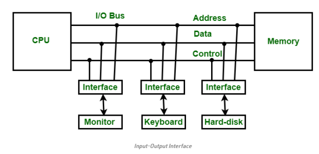
The sole purpose of peripheral devices in a microcomputer-based system is to offer unique communication lines for connecting them with the CPU. Communication links are required to resolve disparities between peripheral devices and the CPU.
The following are the main differences:
1. Peripheral devices are electromagnetic and electromechanical in nature. The CPU is electrical in nature. The modes of functioning of peripheral devices and the CPU differ significantly.
2. Because peripheral devices communicate data at a slower rate than the CPU, there is also a synchronisation mechanism.
3. Data code and formats in peripheral devices differ from those in the CPU and memory
4. Peripheral device operating modes differ, and each can be managed to avoid interfering with the operation of other peripheral devices attached to the CPU.
Additional hardware is required to resolve disparities between the CPU and peripheral devices, as well as to supervise and synchronise all input and output devices.
Functions of Input-Output Interface:
1. It's utilised to keep the CPU's operating speed in sync with the input-output devices.
2. It chooses an input-output device that is appropriate for the input-output device's interpretation.
3. It can send out signals such as control and timing signals.
4. Data buffering is possible through the data bus in this case.
5. There are several types of error detectors.
6. It converts serial data to parallel data and the other way around.
7. It can also convert digital data to analogue signals and the other way around.
4.1.2 Computer Architecture: Input/Output Organisation
Input/Output Subsystem
An efficient way of communication between the central system and the outside environment is provided by a computer's I/O subsystem. It is in charge of the computer system's entire input-output activities.
Peripheral Devices
Peripheral devices are input or output devices that are connected to a computer. These devices, which are considered to be part of a computer system, are designed to read information into or out of the memory unit in response to commands from the CPU. Peripherals are another name for these gadgets.
Consider the following scenario: Keyboards, monitors, and printers are examples of common peripheral devices.
Peripherals are divided into three categories:
1. Input peripherals: These devices allow users to enter data from the outside world into the computer. For instance, a keyboard, a mouse, and so on.
2. Output peripherals: These devices allow data to be sent from the computer to the outside world. For instance, a printer, a monitor, and so on.
3. Input-Output Peripherals: Allows both input (from the outside world to the computer) and output (from the computer to the outside world) (from computer to the outside world). For instance, a touch screen.
Interfaces
A shared boundary between two different components of a computer system that can be used to connect two or more components to the system for communication purposes is known as an interface.
There are two different types of user interfaces:
1. Inteface of the CPU
2. Interface to I/O
Let's take a closer look at the I/O Interface.
Input-Output Interface
For communicating with the CPU, peripherals connected to a computer require particular communication interfaces. In a computer system, there are unique hardware components that govern or regulate input-output transfers between the CPU and peripherals. Because they offer communication links between the CPU bus and peripherals, these components are known as input-output interface units. They provide a means of exchanging data between the internal system and the input-output devices.
4.1.3 Modes of I/O Data Transfer
Data transfer between the central unit and I/O devices can be accomplished in one of three ways, as shown below:
1. Interrupt Initiated I/O
2. Programmed I/O
3. Memory Direct Access
Programmed I/O
I/O instructions written in a computer programme result in programmed I/O instructions. The program's instruction triggers the transfer of each data item.
Typically, the software is in charge of data transport between the CPU and peripherals. Transferring data with programmed I/O necessitates the CPU's ongoing supervision of the peripherals.
Interrupt Initiated I/O
The CPU remains in the programme loop in the programmed I/O approach until the I/O unit indicates that it is ready for data transfer. This is a time-consuming procedure because it wastes the processor's time.
Interrupt started I/O can be used to solve this problem. The interface creates an interrupt when it determines that the peripheral is ready for data transfer. When the CPU receives an interrupt signal, it stops what it's doing and handles the I/O transfer before returning to its prior processing activity.
Direct Memory Access
The speed of transmission would be improved by removing the CPU from the path and allowing the peripheral device to operate the memory buses directly. DMA is the name for this method.
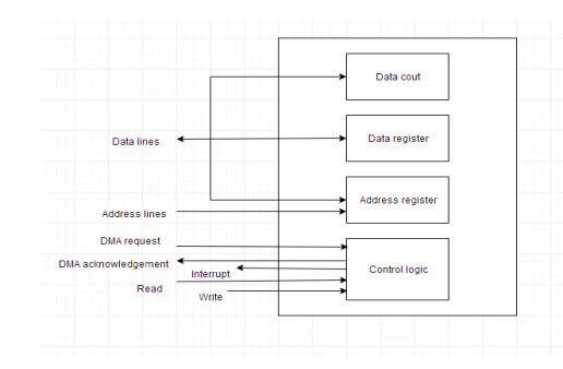
The interface transfers data to and from the memory via the memory bus in this case. A DMA controller is responsible for data transport between peripherals and the memory unit.
DMA is used by many hardware systems, including disc drive controllers, graphics cards, network cards, and sound cards, among others. In multicore CPUs, it's also used for intra-chip data transport. In DMA, the CPU would start the transfer, perform other tasks while it was running, and then get an interrupt from the DMA controller when the transfer was finished.
4.1.4 What is the difference between an input and output device?
An input device transmits data to a computer system, which is then processed, and an output device reproduces or displays the results. Input devices only allow data to be entered into a computer, whereas output devices only receive data from another device.
Because they can either accept data input from a human or emit data created by a computer, most devices are either input or output devices. However, some devices, known as I/O devices (input/output devices), can accept input and show output.
A keyboard, for example, sends electrical signals that are received as input, as illustrated in the top half of the image. The computer then interprets the signals and displays them on the monitor as text or graphics. The computer delivers or outputs data to a printer in the lower half of the image. The data is then printed on a piece of paper, which is also referred to as output.
Input/output (I/O) devices
An input/output device can take data from people or another device (input) and transfer it to another device (output) (output). The following are some examples of input/output devices.
1. CD-RW and DVD-RW drives - These drives receive data from a computer (input) and copy it on a readable CD or DVD. The drive may also send data from a CD or DVD (output) to a computer.
2. USB flash drive - A USB flash drive receives and saves data from a computer (input). The drive can also deliver data to a computer or other device (output).
4.2.1 Random Access Memory (RAM) and Read Only Memory (ROM)
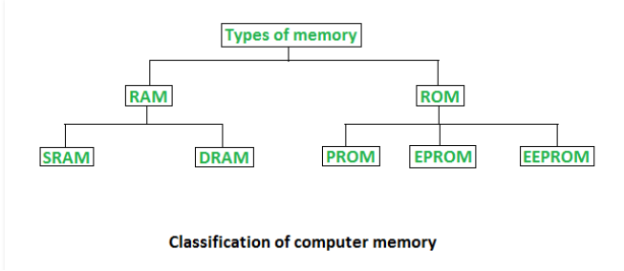
Memory is the most important component of a computer system since it allows it to accomplish simple tasks. There are two types of computer memory: primary memory (RAM and ROM) and secondary memory (hard drive,CD,etc.). Read Only Memory (ROM) is primary-non-volatile memory, while Random Access Memory (RAM) is primary-volatile memory.
1. Random Access Memory (RAM) –
The programmes and data that the CPU requires throughout the execution of a programme are kept in this memory, which is also known as read write memory, main memory, or primary memory.
Because the data is lost when the power is switched off, it is a volatile memory.
SRAM (Static Random Access Memory) and DRAM (Dynamic Random Access Memory) are the two forms of RAM (Dynamic Random Access Memory).
DRAM | SRAM |
1.Constructed of tiny capacitors that leak electricity | 1.Constructed of circuits similar to D flip-flops. |
2.Requires a recharge every few milliseconds to maintain its data. | 2.Holds its contents as long as power is available. |
3.Inexpensive | 3.Expensive
|
4.Slower than SRAM | 4.Faster than DRAM |
5.Can store many bits per chip | 5.Can not store many bits per chip |
6.Uses less power | 6.Uses more power |
7.Generates less heat | 7.Generates more heat |
8.Used for main memory | 8.Used for cache |
2. Read Only Memory (ROM) –
Contains critical information required to operate the system, such as the programme required to start the computer.
It isn't flammable.
It keeps all of its data at all times.
Used in embedded systems or in situations where the programming does not need to be changed.
Calculators and other peripheral devices use it.
ROM is divided into four types: ROM, PROM, EPROM, and EEPROM.
Types of Read Only Memory (ROM) –
- PROM (Programmable read-only memory) – It has the ability to be programmed by the user. The data and instructions in it cannot be modified once they have been programmed.
- EPROM (Erasable Programmable read only memory) – It is reprogrammable. Expose it to ultra violet light to wipe the data on it. Delete all prior data to reprogramme it.
- EEPROM (Electrically erasable programmable read only memory) – The data can be erased without the use of ultra violet light by creating an electric field. Only a piece of the chip can be erased.
Difference between RAM and ROM
RAM | ROM |
1.Temporary storage | 1.Permanent storage |
2.Store data in MBs | 2.Store data in GBs. |
3.Volatile | 3.Non-volatile |
4.Used in normal operations | 4.Used for startup process of computer |
5.Writing data is faster | 5.Writing data is slower |
4.2.2 What is the Difference Between RAM and ROM?
Your computer has both RAM and ROM, which stands for random access memory and read-only memory, respectively.
RAM is a type of volatile memory that stores the files you're working on for a short period of time. Non-volatile memory (ROM) is a type of memory that stores instructions for your computer indefinitely. Learn more about RAM.

Volatile and non-volatile memory
RAM is volatile memory, which means that when you restart or shut down your computer, the information temporarily held in the module is deleted. Because the data is stored electrically on transistors, it vanishes when there is no electric current. When you request a file or piece of information, it is either fetched from the computer's hard drive or from the internet. Because the information is saved in RAM, it is instantaneously available when you transition from one programme or page to another. The memory is wiped when the machine is turned off until the process is restarted. Users can quickly update, upgrade, or extend volatile memory.
Find out if your computer needs more memory.
Non-volatile memory (ROM) is information that is permanently stored on a chip. The memory does not rely on an electric current to save data; instead, binary code is used to write data to individual cells. Non-volatile memory is used for elements of the computer that do not change, such as the software's initial boot-up phase or the firmware instructions that allow your printer to function. The ROM is unaffected by turning off the machine. Users are unable to alter non-volatile memory.
4.2.3 RAM vs ROM: What's the Difference?
What is RAM?
RAM stands for Random Access Memory in its full form. When the power to the PC or laptop is turned off, the information saved in this type of memory is lost. The BIOS can be used to examine the information saved in RAM. It is also known as the computer system's primary memory, temporary memory, cache memory, or volatile memory.
What is ROM?
A Read-Only Memory (ROM) is the full version of the term. It is a form of memory that lasts forever. When the power supply is turned off, the content is not lost. The information in ROM is determined by the computer manufacturer, and it is permanently recorded at the time of production, and it cannot be altered by the user.
Various memory storage devices are compared.
Here's a comparison of several storage devices.
Storage | Speed | Cost | Capacity | Permanent |
Register | Fastest | Highest | Lowest | No |
Hard Disk | Moderate | Very Low | Very High | Yes |
RAM | Very fast | High | Low to Moderate | No |
ROM | Very Fast | High | Very Low | Yes |
CD-ROM | Moderate | Very Low | High | Yes |
4.3.1 Memory
Any physical device capable of temporarily storing information, such as RAM (random access memory), or permanently storing information, such as ROM (read only memory), is referred to as computer memory (read-only memory). Integrated circuits (ICs) are utilised in memory devices, which are used by operating systems, software, and hardware.
What does computer memory look like?
A 512 MB DIMM computer memory module is shown below. This memory module plugs into a computer motherboard's memory slot.

What happens to memory when the computer is turned off?
Because RAM is volatile memory, anything saved in RAM is lost when the computer loses power, as previously stated. For example, a document is stored in RAM while it is being worked on. It would be lost if it was stored to non-volatile memory (e.g., the hard drive) if the computer lost power.
Memory is not disk storage
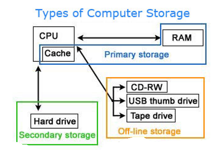
New computer users frequently become perplexed as to which elements of the machine are memory. Although both the hard drive and RAM are memory, RAM should be referred to as "memory" or "primary memory," while the hard drive should be referred to as "storage" or "secondary storage."
When someone asks how much memory your computer has, the answer is usually between 1 and 16 GB of RAM and several hundred gigabytes, if not a terabyte, of hard drive storage. In other words, your hard drive space is always greater than your RAM.
How is memory used?
When you open a programme, such as your Internet browser, it is loaded into RAM from your hard disc. This procedure enables the programme to interface with the processor at a faster rate. Anything you save to your computer, such as a photo or a video, is stored on your hard drive.
Why is memory important or needed for a computer?
Each component of a computer runs at a variable pace, and computer memory allows your computer to retrieve data rapidly. A computer would be substantially slower if the CPU had to wait for a secondary storage device, such as a hard disc drive.
4.3.2 Computer memory
Main memory
Electromechanical switches, or relays (see computers: The First Computer), and electron tubes were the first memory devices (see computers: The first stored-program machines). As main memory, the first stored-program computers utilised ultrasonic waves in mercury tubes or charges in special electron tubes in the late 1940s. These were the world's first random-access memories (RAM). In contrast to serial access memory, such as magnetic tape, RAM comprises storage cells that may be accessed directly for read and write operations, whereas serial access memory, such as magnetic tape, requires accessing each cell in sequence until the required cell is located.
Magnetic drum memory
In the 1950s, magnetic drums were utilised for both primary and auxiliary memory, with fixed read/write heads for each of several tracks on the outside surface of a revolving cylinder coated with a ferromagnetic substance, albeit data access was serial.
Magnetic core memory
Magnetic core memory, an arrangement of microscopic ferrite cores on a wire grid through which current may be routed to change individual core orientations, was created around 1952. Core memory was the primary form of main memory until it was supplanted by semiconductor memory in the late 1960s due to RAM's inherent advantages.
Semiconductor memory
Semiconductor memory is divided into two types. Flip-flops, a bistable circuit made up of four to six transistors, make up static RAM (SRAM). Once a bit is stored in a flip-flop, it remains there until the opposite value is stored in it. SRAM provides quick data access, but it is physically huge. It's mostly utilised in a computer's central processing unit (CPU) for small pieces of memory called registers, as well as for fast "cache" memory. Instead of storing each bit in a flip-flop, dynamic RAM (DRAM) stores each bit in an electrical capacitor, which is charged or discharged using a transistor as a switch. A DRAM storage cell is smaller than an SRAM storage cell because it contains fewer electrical components. However, accessing its value is more time consuming, and because capacitors eventually leak charge, stored values must be recharged 50 times per second. Nonetheless, DRAM is commonly utilised for main memory since it can carry multiple times as much DRAM as SRAM on the same size chip.
Addresses are assigned to storage cells in RAM. It's customary to divide RAM into 8- to 64-bit "words," or 1 to 8 bytes (8 bits = 1 byte). The size of a word refers to the maximum number of bits that can be transmitted between main memory and the CPU at one time. Every word and, in most cases, every byte has a unique address. Additional decoding circuits are required on a memory chip to choose the set of storage cells at a given address and either save or retrieve the value stored there. A modern computer's primary memory is made up of a number of memory chips, each of which can carry many megabytes (millions of bytes), with additional addressing hardware selecting the correct chip for each address. DRAM also necessitates circuits to detect and refresh its stored values on a regular basis.
It takes longer for main memories to obtain data than it does for CPUs to work on them. DRAM memory access, for example, typically takes 20 to 80 nanoseconds (billionths of a second), but CPU arithmetic operations can take as little as a nanosecond. This inequality can be addressed in a number of ways. CPUs have a limited amount of registers and need very fast SRAM to store current instructions and data. Cache memory is a bigger amount of quick SRAM on the CPU chip (up to several gigabytes). Data and instructions from main memory are copied into the cache, and because programmes frequently exhibit "locality of reference"—that is, they repeatedly execute the same instruction sequence and operate on sets of related data—memory references to the fast cache can be made once values are copied into it from main memory.
Decoding the address to select the proper storage cells takes up a lot of DRAM access time. Because of the locality of reference property, a set of memory addresses will be frequently accessed, and fast DRAM is designed to speed up access to successive addresses following the first. SDRAM (synchronous dynamic random access memory) and EDO (extended data output) are two examples of rapid memory.
Unlike SRAM and DRAM, nonvolatile semiconductor memories do not lose their contents when the power is switched off. Read-only memory (ROM), for example, is not rewritable once it has been produced or written. A transistor is present in each memory cell of a ROM chip for a 1 bit and none for a 0 bit. The bootstrap software that starts a computer and loads its operating system, or the BIOS (basic input/output system) that addresses external devices in a personal computer, are examples of programmes that are fundamental aspects of a computer's function (PC).
EPROM (erasable programmable ROM), EAROM (electrically alterable ROM), and flash memory are examples of rewritable nonvolatile memories, however rewriting takes significantly longer than reading. They are thus utilised as special-purpose memories where writing is rarely required—for example, they can be altered to fix faults or update functionality if utilised for the BIOS.
Auxiliary memory
Auxiliary memory units are one type of computer peripheral. They give up faster access speeds in exchange for more storage capacity and data consistency. Auxiliary memory stores programmes and data for later use It is used to save inactive programmes and archive data because it is nonvolatile (like ROM). Punched paper tape, punched cards, and magnetic drums were all early forms of supplementary storage. Magnetic discs, magnetic tapes, and optical discs have been the most frequent forms of supplementary storage since the 1980s. Auxiliary memory units are one type of computer peripheral. They give up faster access speeds in exchange for more storage capacity and data consistency. Auxiliary memory stores programmes and data for later use It is used to save inactive programmes and archive data because it is nonvolatile (like ROM). Punched paper tape, punched cards, and magnetic drums were all early forms of supplementary storage. Magnetic discs, magnetic tapes, and optical discs have been the most frequent forms of supplementary storage since the 1980s.
Magnetic disk drives
A magnetic substance, such as iron oxide, is used to cover magnetic discs. Hard discs, which are made of rigid aluminium or glass, and removable diskettes, which are made of flexible plastic, are the two sorts. The first magnetic hard drive (HD) was developed by IBM in 1956, and it consisted of 50 21-inch (53-cm) discs with a storage capacity of 5 megabytes. By the 1990s, the standard HD diameter for PCs had reduced to 3.5 inches (about 8.9 cm), with storage capacity exceeding 100 gigabytes (billions of bytes); the usual HD size for portable PCs (“laptops”) had decreased to 2.5 inches (about 8.9 cm) (about 6.4 cm). Diskettes have shrunk from 8 inches (approximately 20 cm) to the current norm of 3.5 inches since Alan Shugart invented the floppy disc drive (FDD) at IBM in 1967. (about 8.9 cm). Since the introduction of optical disc drives in the 1990s, FDDs have become outdated due to their limited capacity (usually less than two megabytes).
The entire assembly is known as a comb, and it consists of numerous discs, or platters, with an electromagnetic read/write head for each surface. The heads are controlled by a microcontroller in the drive, which also incorporates RAM for data transfer to and from the discs. The heads move around the disc surface as it spins at up to 15,000 RPM; the drives are hermetically sealed, allowing the heads to float on a thin film of air near the disk's surface. A small current is provided to the head to magnetise tiny areas on the disc surface for storage; similarly, as the head travels by, magnetised places on the disc generate currents in the head, allowing data to be read. FDDs work in a similar way, although the removable diskettes only rotate at a few hundred times each minute.
The read/write heads must be controlled very precisely since the data is stored in near concentric grooves. Refinements in head control have allowed for smaller and closer track packing—up to 20,000 tracks per inch (8,000 tracks per centimetre) at the turn of the century—resulting in a nearly 30 percent increase in storage capacity per year since the 1980s. RAID (redundant array of cheap discs) is a technology that combines many disc drives to store data redundantly for increased reliability and access speed. High-performance computer network servers employ them.
Magnetic tape
Magnetic tape, like the tape used in tape recorders, has been utilised for supplementary storage, especially for data preservation. Because tape is sequential-access memory, data must be read and written sequentially as the tape is unwound, rather than being retrieved directly from the desired spot on the tape, access time is much slower than that of a magnetic disc. Servers can also use vast collections of cassettes or optical discs, which are selected and loaded by robotic devices, similar to old-fashioned jukeboxes.
Optical discs
The optical compact disc, which was derived from videodisc technology in the early 1980s, is another form of mostly read-only memory. Data is recorded as tiny pits on a single spiral track on plastic discs ranging in diameter from 3 to 12 inches (7.6 to 30 cm), however the most frequent diameter is 4.8 inches (12 cm). A low-power laser and a photocell that generates an electrical signal from the fluctuating light reflected from the pattern of pits produce the pits, which are read by a low-power laser and a photocell. Optical discs are detachable and have significantly more memory capacity than diskettes; the larger ones may hold hundreds of gigabytes of data.
The CD-ROM is a common optical disc (compact disc read-only memory). It can store around 700 megabytes of data and uses an error-correcting code to rectify bursts of errors generated by dust or flaws. Software, encyclopaedias, and multimedia text with sounds and images are all distributed on CD-ROMs. CD-R (CD-recordable) or WORM (write-once read-many) is a type of CD-ROM that allows users to record data but not change it later. Rewritable CD-RW discs can be re-recorded. DVDs (digital video, or versatile, discs), originally designed for recording movies, store data more densely and with more powerful error correction than CD-ROM. DVDs, which are the same size as CDs, typically carry 5 to 17 terabytes of data—several hours of video or millions of text pages.
Magneto-optical discs
Hybrid storage media are magneto-optical discs. In reading, variable polarisation in the reflected light of a low-power laser beam is caused by spots with various magnetization directions. To write all 0s, a powerful laser beam heats each area on the disc, which is subsequently cooled under a magnetic field, magnetising each spot in one direction. The writing operation then reverses the magnetic field's direction to store 1s at the desired location.
Memory hierarchy
Although the distinction between main and auxiliary memory is useful in general, memory organisation in a computer is organised in a hierarchy of levels, starting with very small, fast, and expensive registers in the CPU and progressing to small, fast cache memory, larger DRAM, very large hard discs, and slow and inexpensive nonvolatile backup storage. Virtual memory, a system that provides programmes with huge address spaces (addressable memory) that may surpass the real RAM in the machine, spans these levels in memory consumption by modern computer operating systems. Virtual memory allots a piece of main memory to each application while storing the remainder of its code and data on a hard disc, transferring blocks of addresses to and from main memory as needed. Virtual memory is possible thanks to the speed of current hard discs and the same locality of reference principle that allows caches to perform well.
Coprocessor, a specialised processor found in some personal computers that performs tasks such as intensive mathematical calculations or graphical display processing. The coprocessor is frequently built to perform such jobs more efficiently than the main processor, resulting in much faster computer performance overall.
Flash memory
Computers and other electronic equipment use flash memory as a data storage medium. Flash memory, unlike prior kinds of data storage, is an EEPROM (electronically erasable programmed read-only memory) type of computer memory that does not require a power source to preserve data.
Masuoka Fujio, a Japanese engineer at the time working for Toshiba Corporation, devised flash memory in the early 1980s as a technique to replace existing data-storage medium such as magnetic tapes, floppy discs, and dynamic random-access memory (DRAM) chips. Ariizumi Shoji, a Masuoka coworker, developed the term flash after comparing the process of memory erasure, which can delete all the data on a complete chip at once, to a camera's flash.
Flash memory is made up of a grid with two transistors at each intersection, the floating gate and the control gate, separated by an oxide layer that insulates the floating gate. The two-transistor cell has a value of 1 when the floating gate is connected to the control gate. A voltage is applied to the control gate, which drives electrons through the oxide layer into the floating gate, changing the cell's value to 0. The floating gate stores the electrons, allowing the flash memory to maintain its data even after the power is switched off. To return the value to 1, a voltage is delivered to the cell. Large parts of a chip, known as blocks, or even the entire chip can be wiped at once when using flash memory.
Flash memory is commonly used in portable devices such as digital cameras, smartphones, and MP3 players. Flash memory is used to store data on USB devices (also known as thumb drives or flash drives) and memory cards. As flash memory became more affordable in the early twenty-first century, it began to replace hard discs in laptop computers.
4.3.3 Types of Computer Memory
Computer memory refers to the various forms of data storage technology that a computer can employ, such as RAM, ROM, and flash memory.
Some computer memory is designed to be extremely fast, allowing the central processor unit (CPU) to quickly retrieve data stored there. Other varieties are meant to be extremely low-cost, allowing enormous volumes of data to be stored there without breaking the bank.
Another difference in computer memory is that some types are non-volatile, meaning they can keep data for a long time even after the power is turned off. And then there are volatile varieties, which are generally speedier but lose all of the data they contain as soon as the power is turned off.
A computer system is made up of a mix of various types of computer memory, and the exact arrangement can be tweaked to achieve the best data processing speed, lowest cost, or a compromise between the two.
Types of Computer Memory: Primary and Secondary
Although there are many different types of memory in a computer, the most basic distinction is between primary memory, also known as system memory, and secondary memory, often known as storage.
The main distinction between primary and secondary memory is access speed.
Primary memory
Includes ROM and RAM, and is located close to the CPU on the computer motherboard, enabling the CPU to read data from primary memory very quickly indeed. It is used to store data that the CPU needs imminently so that it does not have to wait for it to be delivered.
Secondary memory
Data, on the other hand, normally housed in a separate storage device, such as a hard disc drive or solid state drive (SSD), that is connected to the computer system either directly or over a network. Secondary memory has a lower cost per gigabyte, but read and write speeds are much slower.
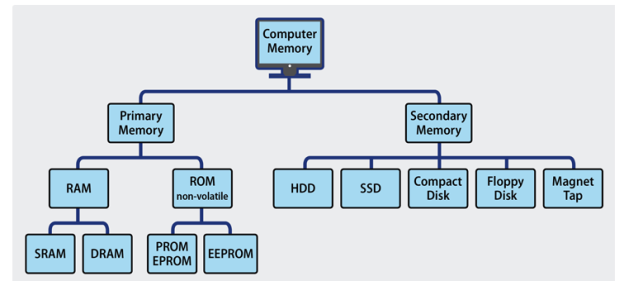
A diverse range of computer memory types has been used during the course of computer evolution, each with its own set of strengths and disadvantages.
Primary Memory Types: RAM and ROM
Primary memory can be divided into two categories:
1. RAM (random access memory) is a type of memory that is used to store data.
2. Read-only memory (ROM)
Let's take a closer look at both types of memory.
1) RAM Computer Memory
The abbreviation RAM refers to the fact that data stored in random access memory can be accessed in any order, as the name suggests. To put it another way, any random bit of data can be retrieved in the same amount of time as any other bit.
The most important things to know about RAM memory are that it is very fast, that it can be written to as well as read, that it is volatile (that is, all data stored in RAM memory is lost when it loses power), and that it is very expensive in terms of cost per gigabyte when compared to all other types of secondary memory. Most computer systems use both primary and secondary memory due to the relative high cost of RAM compared to secondary memory types.
Data that needs to be processed right away is relocated to RAM, where it can be read and updated rapidly, keeping the CPU from having to wait. When the data is no longer needed, it is moved to slower but less expensive secondary memory, and the RAM space that is freed up is filled with the next chunk of data to be used.
Types of RAM
- DRAM: The most popular type of RAM used in computers is DRAM, which stands for Dynamic RAM. Single data rate (SDR) DRAM is the oldest form, however modern systems employ quicker dual data rate (DDR) DRAM. DDR is available in numerous variants, including DDR2, DDR3, and DDR4, all of which are faster and more energy efficient than DDR. However, because the two versions are incompatible, DDR2 and DDR3 DRAM cannot be mixed in a computer system. Each cell of DRAM contains a transistor and a capacitor.
2. SRAM: SRAM stands for Static RAM, and it is a form of RAM that is faster than DRAM but more expensive and bulkier because each cell has six transistors. As a result, SRAM is typically only employed as a data cache within a CPU or as RAM in extremely high-end server systems. In a system 3, a modest SRAM cache of the most urgently needed data can result in significant speed benefits. SRAM is two to three times faster than DRAM, although it is more expensive and bulkier. SRAM is often sold in megabytes, whereas DRAM is sold in gigabytes.
3. DRAM consumes more energy than SRAM because it must be refreshed on a regular basis to ensure data integrity, but SRAM, while volatile, does not require constant refreshing while powered up.
2) ROM (Read Only Memory)
ROM stands for read-only memory, and it gets its name from the fact that data may be read from but not written to this type of computer memory. It is a form of computer memory that is located near the CPU on the motherboard and is extremely fast.
ROM is a sort of non-volatile memory, which implies that the data contained in it persists even after the computer is turned off and no power is applied to it. It's comparable to secondary memory in that it's utilised for long-term storing.
When a computer is turned on, the CPU can immediately begin reading data from the ROM without the need for drivers or other complicated software. The ROM typically contains "bootstrap code," which is a series of instructions that a computer must follow to become aware of the operating system stored in secondary memory and to load components of the operating system into main memory so that it can start up and become ready to use.
Simpler electronic devices use ROM to store firmware that executes as soon as the device is turned on.
Types of ROM
PROM, EPROM, and EEPROM are some of the numerous types of ROM accessible.
1. PROM PROM stands for Programmable Read-Only Memory, and it differs from genuine ROM in that a PROM is built in an empty state and then programmed later using a PROM programmer or burner, whereas a ROM is programmed (that is, data is written to it) during the production process.
2. EPROM EPROM stands for Erasable Programmable Read-Only Memory, and data saved in an EPROM may be erased and reprogrammed, as the name implies. Before re-burning an EPROM, it must be removed from the computer and exposed to ultraviolet light.
3. EEPROM (Electronic Flash Memory) The difference between EPROM and EEPROM, which stands for Electrically Erasable Programmable Read-Only Memory, is that the latter may be erased and written to by the computer system in which it is installed. EEPROM is not strictly read-only in this sense. However, because the write process is slow in many circumstances, it is usually reserved for updating programme code such as firmware or BIOS code on a sporadic basis.
Despite the fact that NAND flash memory (such as that found in USB memory sticks and solid state disc drives) is a kind of EEPROM, it is classified as secondary memory.
4.3.4 Secondary Memory Types
Secondary memory refers to a variety of storage devices that can be directly connected to a computer system. Hard disc drives and solid state drives are examples of this (SSDs)
Optical drives (CD or DVD)
Drives for tapes
Secondary memory also includes: Storage arrays connected via a storage area network, including 3D NAND flash arrays (SAN)
Storage devices that can be connected through a standard network (known as network attached storage, or NAS)
Cloud storage is also referred to as "secondary memory."
Differences between RAM and ROM
ROM:
1. The term "non-volatile" refers to a substance that is
2. Easy to read
3. Only used in little amounts
4. Cannot be written in a short period of time
5. It's where you keep your boot instructions or firmware.
6. When compared to RAM, per megabyte stored is relatively expensive.
RAM:
1. Fluctuating
2. Read and write quickly
3. Used as system memory to store data (including computer code) that the CPU must process as soon as possible.
4. In comparison to ROM, it is reasonably inexpensive per megabyte stored, but it is relatively expensive in comparison to secondary memory.
What Technology is Between Primary and Secondary Memory?
A novel memory medium dubbed 3D XPoint has been invented in the last year or two, with features that fall in between main and secondary memory.
3D XPoint is more expensive than secondary memory but faster, and less expensive but slower than RAM. It's also a sort of non-volatile memory.
Because of these qualities, it can be used as a replacement for RAM in systems that require large amounts of system memory but are too expensive to develop using RAM (such as systems hosting in-memory databases). The trade-off is that such systems do not benefit from all of RAM's performance benefits.
Because 3D XPoint is non-volatile, systems that utilise it for system memory can quickly recover from a power outage or other interruption, without having to read all of the data back into system memory from secondary memory.
Key takeaway:
Memory is a mechanism or system for storing data in a computer or other computer hardware and digital electrical devices for immediate use. The terms memory and major storage or main memory are frequently used interchangeably. The word store is an old synonym for memory.
4.4.1 Memory Organization and Addressing
Now we'll take a look at RAM, or Random Access Memory. This is the memory known as "primary memory" or "core memory," which refers to an earlier memory technology in which magnetic cores were utilised to store data on the computer.
The best way to think of primary computer memory is as an array of addressable units. The smallest unit of memory with independent addresses is called an addressable unit. Each byte (8 bits) in a byte-addressable memory unit has its own address, though the computer frequently groups the bytes into larger units (words, long words, etc.) and retrieves that group. In most modern computers, integers are manipulated as 32-bit (4-byte) entities, therefore they are retrieved four bytes at a time.
Byte addressing in computers became crucial, in this author's viewpoint, as a result of the adoption of 8-bit character codes. Many applications benefit from the ability to address single characters because they entail the movement of huge numbers of characters (coded as ASCII or EBCDIC). Word addressing is used by some computers, including the CDC-6400, CDC-7600, and all Cray machines. This is the outcome of a design decision taken when considering the fundamental objective of such computers, which is to perform huge computations using floating point values. The word size in these computers is 60 bits (why not 64? - I'm not sure), which allows for high precision in numeric simulations like fluid flow and weather forecasting.
Memory as a Linear Array
Consider a memory with N bytes of byte-addressable memory. As previously indicated, such a memory can be thought of as the logical equivalent of a C++ array, and is declared as byte memory [N] ; / Address ranges from 0 to (N – 1)
The machine on which these notes were written has 384 MB of main RAM, which is now considered standard but was originally considered enormous. N = 384•1048576 = 402,653,184 because 384 MB = 384•220 bytes and the memory is byte-addressable. The memory size is frequently a power of two or the sum of two powers of two; (256 + 128)•220 = 228 + 227 = 384 MB
When it comes to computer memory, the term "random access" suggests that memory can be accessed at any time with no performance penalty. While this may not be exactly accurate in these days of virtual memory, the basic concept remains the same: the time it takes to access an item in memory is independent of the address provided. In this way, it's analogous to an array in which the time it takes to retrieve a particular entry is independent of the index. A magnetic tape is a sequential access technology, which means that in order to get to an entry, you must first go through all of the previous entries.
Random-access computer memory is divided into two categories. These are the following:
RAM Read-Write Memory
ROM Read-Only Memory
The use of the term "RAM" to refer to a sort of random access memory that might be referred to as "RWM" has a lengthy history, which will be continuing in this course. The main reason is that the names "RAM" and "ROM" are simple to pronounce; try saying "RWM." Keep in mind that random access memory (RAM) and read-only memory (ROM) are the same thing.
Of course, there is no such thing as a pure Read-Only memory; data must be able to be written to the memory at some point in order for it to be read; otherwise, there will be no data in the memory to read. The term "Read-Only" mainly relates to how the CPU accesses data. All ROM variants have the property that standard CPU write operations cannot change their contents. All types of RAM (also known as Read-Write Memory) have the ability to update their contents using standard CPU write operations. Some types of ROM have their contents pre-programmed, while others, known as PROM (Programmable ROM), can have their contents modified using special devices known as PROM Programmers.
Registers associated with the memory system
Two registers and a number of control signals characterise all memory types, including RAM and ROM. Consider a memory with 2N words and M bits per word. Then there's the MAR (Memory Address Register), which is an N-bit register that specifies the memory address.
The MBR (Memory Buffer Register) is a multi-bit register that stores data for later use be written to the memory or simply read from it This is a registry also known as the MDR (Memory Data Register).
We tell the memory unit what to do with the control signals by recalling what we want it to perform. Consider RAM first (Read Write Memory). There are three duties for memory from the CPU's perspective.
Data is read from memory by the CPU. The contents of the memory are not altered.
Data is written to memory by the CPU. The contents of the memory are updated.
Memory is not accessed by the CPU. The contents of the memory are not altered.
Two control signals are required to indicate the three RAM unit possibilities. There is a standard set.
The memory unit has been selected.
- If 0 is set, the CPU writes to memory; if 1 is set, the CPU reads from it.
A truth table can be used to indicate the activities for a RAM. It's worth noting that when Select = 0,
Select | R/  | Action |
0 | 0 | Memory contents are not changed. |
0 | 1 | Memory contents are not changed. |
1 | 0 | CPU writes data to the memory. |
1 | 1 | CPU reads data from the memory. |
The memory is not being affected in any way. The CPU does not access it, and the contents do not change. When Select is set to 1, the memory is activated, and something occurs.
Now is the time to think about a ROM (Read Only Memory). There are just two duties for memory from the CPU's perspective.
Data is read from memory by the CPU.
Memory is not accessed by the CPU.
To indicate these two possibilities, we just need one control signal. The Select control signal is a natural choice because the signal makes no sense if the memory can't be written by the CPU. The ROM's truth table should be self-evident.
Select | Action |
0 | CPU is not accessing the memory. |
1 | CPU reads data from the memory. |
4.4.2 The Idea of Address Space
Now it's time to separate the concepts of address space and physical memory. The address space specifies the range of addresses (memory array indices) that can be created. Physical memory is typically smaller, either by design (see the topic of memory-mapped I/O below) or by chance.
2N distinct addresses are specified using a N–bit address. In this respect, the address can be thought of as an unsigned N–bit integer with a range of 0 to 2N – 1 inclusive. Another concern is how many address bits are required for M addressable things. The equation 2(N - 1) M 2N gives the result, which is best solved by guessing N.
A binary number stored in the Memory Address Register specifies the memory address (MAR). The range of addresses that can be created is determined by the number of bits in the MAR. 2N different addresses, numbered 0 through 2N – 1, can be specified using N address lines. This is referred to as the computer's address space.
We present three MAR sizes as an example.
Computer | MAR bits | Address Range |
PDP-11/20 | 16 | 0 to 65 535 |
Intel 8086 | 20 | 0 to 1 048 575 |
Intel Pentium | 32 | 0 to 4 294 967 295 |
The now-defunct Digital Equipment Corporation produced the PDP-11/20, an exquisite little machine. People noticed that its address range was too limited as soon as it was built.
The address space is, on average, substantially bigger than the physical memory accessible. My personal computer, for example, has a 232-byte address space (as do all Pentiums), but only 384MB = 228 Plus 227 bytes. The 32–bit address space would have been significantly greater than any quantity of physical memory until recently. Currently, a computer with a fully loaded address space, i.e. 4 GB of physical memory, may be ordered from a variety of vendors. The majority of high-end personal PCs come with 1GB of RAM
A portion of the address space in an architecture with memory-mapped I/O is allocated to addressing I/O registers rather than physical memory. The top 4096 (212) of the address space on the original PDP–11/20, for example, was dedicated to I/O registers, leading to the memory map
0 – 61439 is a range of addresses. Physical memory is available.
61535, 61440, 61440, 61440, 61440, 61440, 61440, I/O registers (61440 = 61536 – 4096) are available.
In a byte-addressable machine, word addresses are used.
Most modern computers have byte-addressable memories, which means that each byte in the memory has a unique address that may be used to address it. A word corresponds to a number of addresses in this addressing method.
Bytes at addresses Z and Z + 1 make up a 16–bit word at address Z
Bytes at addresses Z, Z + 1, Z + 2, and Z + 3 make up a 32–bit word at address Z.
Word addresses are constrained on many computers that use byte addressing.
An even address is required for a 16–bit word.
The address of a 32–bit word must be a multiple of four.
It's a good idea to stick to these word boundaries even if your computer doesn't demand it. Most compilers will do this for you.
Consider a machine having a 32-bit address space and byte-addressable memory. 232 − 1 is the highest byte address. We can deduce from this fact and the address allocation to multi-byte words that
(232 – 2) is the highest address for a 16-bit word, and
Because the 32-bit word addressed at (232 – 4) contains bytes at addresses (232 – 4), (232 – 3), (232 – 2), and (232 – 1), the highest address for a 32-bit word is (232 – 4).
4.4.3 Byte Addressing vs. Word Addressing
N address lines can be used to specify 2N separate addresses, numbered 0 through 2N – 1. As previously stated, N address lines can be used to define 2N separate addresses, numbered 0 through 2N – 1. We've moved on to enquiring about the size of the addressable items. Most current computers are byte-addressable, which means that the addressable item is 8 bits or one byte in size. Other options are available. We'll now look at the benefits and drawbacks of being able to address larger entities.
Consider a computer with a 16–bit address space as an example. There would be 65,536 (64K = 216) addressable entities on the system. The maximum memory size is determined by the addressable entity's size.
64 KB of byte addressable memory
128 KB, 16-bit Word Addressable
256 KB, 32-bit Word Addressable
The maximum memory size for a given address space is greater for larger addressable entities. This may be advantageous for some applications, but it is mitigated by the extremely huge address spaces we already have: 32 bits now, 64 bits soon.
When we consider programmes that process data one byte at a time, the benefits of byte-addressability become evident. In a byte-addressable system, accessing a single byte needs simply issuing a single address. In a 16-bit word-addressable system, computing the address of the word containing the byte, fetching that word, and finally extracting the byte from the two-byte word are all required steps. Although byte extraction procedures are well understood, they are less efficient than retrieving the byte directly. As a result, many current machines can be addressed in bytes.
4.4.4 Big-Endian and Little-Endian
The connection here is to a storey in Jonathan Swift's Gulliver's Travels about two groups of men fighting over whether the big end or the little end of a boiled egg should be broken. Swift's work A Modest Proposal is an outstanding example of biting satire; the student should be aware that he did not write pleasant stories for children, but instead focused on cutting satire.
Consider the 32–bit number stored at memory location Z, which is represented by the eight–digit hexadecimal number 0x01020304. This number will be stored in the four successive addresses Z, (Z + 1), (Z + 2), and (Z + 3) in all byte-addressable memory regions. The location of each of the four bytes differs between big-endian and little-endian addresses. Bits 31–24 are represented by 0x01, and bits 23–16 are represented by 0x02.
Bits 15–8 of the word are represented by 0x03, and bits 7–0 of the word are represented by 0x04.
The number 0x01020304 can be written in decimal notation as a 32-bit signed integer.
1•166 + 0•165 + 2•164 + 0•163 + 3•162 + 0•161 + 4•160 = 16,777,216 + 131,072 + 768 + 4 = 16,909,060. 1•166 + 0•165 + 2•164 + 0•163 + 3•162 + 0•161 + 4•160 = 16,777,216 + 131,072 + 768 + 4 = 16,909,060 If you want to think in bytes, this is (01)•166 + (02)•164 + (03)•162 + 04, which gives you the same result. It's worth noting that the number can be considered as having a "large end" and a "small end," as shown in the diagram below.

The “big end” of the number contains the most significant digits, while the “little end” contains the least important digits. Now we'll look at how these bytes are saved in byte-addressable memory. Remember that each byte in a byte-addressable memory has a unique address consisting of two hexadecimal numbers, and that a 32-bit (four-byte) entry at address Z fills the bytes at Z, (Z + 1), (Z + 2), and (Z + 3). Below are the hexadecimal values saved in these four byte addresses.
Address Big-Endian Little-Endian
Z 01 04
Z + 1 02 03
Z + 2 03 02
Z + 3 04 01
Consider the 16–bit number 0A0B, which is represented by the four hex digits 0A0B. Assume that the 16-bit word is located at W; that is, its bytes are located at W and (W + 1). 0x0A is the most significant byte, whereas 0x0B is the least significant byte. Below are the values for the two addresses.
Address Big-Endian Little-Endian
W 0A 0B
W + 1 0B 0A
The diagram below illustrates a graphical representation of these two ordering alternatives for bytes copied from a register into memory. We'll use a 32-bit register with bits numbered 31 through 0 as an example. Which end of the memory is placed first – at address Z? The “big end,” or most significant byte, is written first in big-endian. The “little end,” or least significant byte, is written first in little-endian.

There does not appear to be any benefit to one system over the other. Most people find big–endian more natural, and it makes reading hex dumps (listings of a sequence of memory addresses) easier, though a decent debugger will take care of it for everyone except the unlucky.
The IBM 360 series, Motorola 68xxx, and Sun SPARC are all big-endian computers.
The Intel Pentium and similar computers are examples of little-endian computers.
Most of us aren't immediately affected by the big-endian vs. Little-endian argument. Allow the computer to handle the bytes in whichever sequence it wants as long as the results are good. The only immediate impact on the majority of us will be when trying to transfer data from one machine to another. The fact that network interfaces for computers will translate to and from the network standard, which is big-endian, makes transfer over computer networks easier. The most challenging part will be trying to read various file kinds.
When computer data is “serialised,” or written out one byte at a time, the big-endian vs. Little-endian dispute shows up in file structures. This results in distinct byte orders for the same data, similar to the memory ordering. The file structure's orientation is frequently determined by the system on which the software was first built.
This is a brief list of file types extracted:
Windows BMP, MS Paintbrush, MS RTF, and GIF (little-endian)
Big-endian data types JPEG, MacPaint, Adobe Photoshop
Some apps support both orientations, with a flag in the header record indicating the order in which the file was written.
4.4.5 The Memory Hierarchy
Depending on the point we're trying to make, we employ a variety of logical models of our memory system. The most basic form of memory is a monolithic linear memory, which is a memory that is made up of a single unit (monolithic) and structured as a single-dimensional array (linear). As a logical model, this is adequate, but it misses a large number of critical concerns.
Consider a memory in which the smallest addressable unit is a M–bit word. For the sake of simplicity, we'll suppose that the memory has N = 2K words and that the address space has N = 2K words as well. The memory can be thought of as a one-dimensional array with a name like
Memory: M–bit word array [0.. (N – 1)].
The monolithic view of the memory is shown in the following figure.
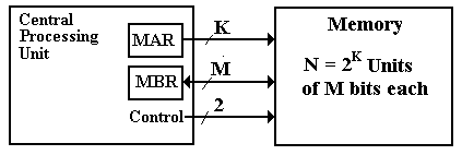
Figure: Monolithic View of Computer Memory
The CPU offers K address bits to access N = 2K memory entries, each with M bits, and at least two control signals to manage memory in this monolithic perspective.
The linear perspective of memory is a rational way of thinking about memory organisation. This viewpoint has the virtue of being straightforward, but it has the problem of accurately defining only long-since-obsolete technologies. It is, nevertheless, a consistent model worth mentioning. The linear model is depicted in the diagram below.
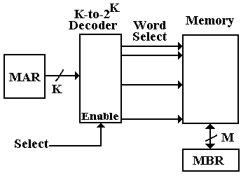
The aforementioned model has two flaws, one of which is a slight annoyance and the other of which is a "show–stopper."
The only small issue is the memory's speed; it will have the same access time as standard DRAM (dynamic random access memory), which is roughly 50 nanoseconds. We know we can do better than that, so we seek out other memory organisations.
The memory decoder's design is the "show–stopper" challenge. Consider two popular memory sizes in byte–oriented memory: 1MB (220 bytes) and 4GB (232 bytes).
A 20–to–1,048,576 decoder would be used for a 1MB memory, because 220 = 1,048,576.
A 32–to–4,294,967,296 decoder would be used in a 4GB memory, because 232 = 4,294,967,296.
With current technology, neither of these decoders can be produced at a reasonable cost. It is important to highlight that because other designs provide extra benefits, there is no incentive to complete such a design work.
Now we'll look at two design options that result in simple-to-manufacture systems with adequate performance at a fair cost. The first is a memory hierarchy that uses different levels of cache memory to provide faster access to main memory. Before delving into the concepts of cache memory, it's necessary to first explain two memory fabrication methodologies.
4.4.6 SRAM (Static RAM) and DRAM (Dynamic RAM)
Now we'll look at the technologies that are used to store binary data. The first topic is to create a list of requirements for binary memory implementation devices.
1) Two separate and well-defined states.
2) The gadget must be able to dependably swap states.
3) A spontaneous state shift must have a very low probability.
4) State transitions must be as quick as possible.
5) The device must be tiny and inexpensive in order for huge memory capacities to be viable.
In the second half of the twentieth century, a variety of memory technologies were developed. The majority of these are no longer in use. There are three that deserve special attention:
1) Memory at the Core (now obsolete, but new designs may be introduced soon)
2) RAM that is static
3) RAM that is dynamic
Core Memory
When it was initially utilised on the MIT Whirlwind in 1952, it was a significant advancement. A torus (small doughnut) of magnetic material serves as the basic memory element. A magnetic field in one of two directions can be contained within this torus. These two separate ways enable a two-state device, which is necessary for storing a binary number.
One characteristic of magnetic core memory has stuck with us: the phrase "core memory" is frequently used as a synonym for the computer's primary memory.
Two definitions are required when considering the next two technologies. Memory access time and memory cycle time are two of them. The access time is a measure of true interest. The nanosecond, or one billionth of a second, is the unit of measurement for memory times.
Memory access time is the time it takes for the memory to access data; more precisely, it is the time it takes for the memory address in the MAR to become stable and the data to become available in the MBR.
The minimal time between two independent memory accesses is known as memory cycle time. Because the memory cannot process an independent access while it is in the process of depositing data in the MBR, the cycle time must be at least as long as the access time.
Static RAM
The minimal time between two independent memory accesses is known as memory cycle time. Because the memory cannot process an independent access while it is in the process of depositing data in the MBR, the cycle time must be at least as long as the access time.
Dynamic RAM
DRAM stands for dynamic random access memory and is based on capacitors, which are circuit elements that hold electric charge. Dynamic RAM is less expensive than static RAM and may fit more tightly on a computer chip, allowing for greater memory capacities. DRAM has a slower access time than SRAM, ranging from 60 to 100 nanoseconds.
Our goal in memory design would be to produce a memory unit with SRAM-like performance but DRAM-like cost and package density. Thankfully, this is possible because to a design technique known as "cache memory," in which a fast SRAM memory serves as a front end for a bigger and slower DRAM memory. Because of a feature of computer programme execution known as "programme locality," this approach has been discovered to be advantageous. If a programme accesses a memory location, it is very likely that it will access that site again, as well as places with similar addresses. Cache memory is made possible by programme locality.
The Memory Hierarchy
In general, the memory hierarchy of a modern computer is as shown in the next figure.

Figure: The Memory Hierarchy with Cache and Virtual Memory
A multi-level memory system has a quicker primary memory and a slower secondary memory, according to our definition. The cache is the speedier primary memory, while the main memory is the secondary memory in cache memory. In this chapter, we'll disregard virtual memory.
It was common practise in early computer designs to include a single-level fast cache in order to boost computer performance. This cache was built on a memory chip that was physically close to the CPU. It became possible to add additional cache that was physically on the CPU chip as succeeding designs enhanced the circuit density on the CPU chip. The Intel Pentium designs now have a two-level cache, such as the following.
L1 cache of 32 KB (Level 1 cache with 16KB for instructions and 16KB for data)
L2 cache of 1 MB (Level 2 cache for both data and instructions)
Main memory: 256 MB
For a given technology, the argument for a two–level cache is based on the idea that smaller memories have a faster access time than bigger memories. It's easy to show that a two–cache (32 KB and 1MB) has a far faster effective access time than a monolithic cache of about 1MB.
4.4.7 Effective Access Time for Multilevel Memory
The success of a multilevel memory system is based on the notion of locality, as we previously established. The hit ratio, which is represented in the memory system's effective access time, is a measure of the system's effectiveness.
A multilayer memory system with primary and secondary memory will be considered. We can use what we've learned so far to both cache memory and virtual memory systems. We'll use cache memory as an example in this lesson. This is something that might be readily adapted to virtual memory.
An accessible item in a conventional memory system is referred to by its address. In a two-level memory system, the address is first examined in primary memory. We have a hit if the referenced item is in the primary memory; otherwise, we have a miss. The hit ratio is calculated by dividing the total number of memory accesses by the number of hits; 0.0 h 1.0. We calculate the effective access time as a function of the hit ratio for a quicker primary memory with an access time TP and a slower secondary memory with an access time TS. TE = h•TP + (1.0 – h)•TS is the formula to use.
RULE: In this formula we must have TP < TS. This inequality defines the terms “primary” and “secondary”. In this course TP always refers to the cache memory.
We'll use cache memory as an example, with a fast cache serving as a front-end for primary memory. Cache hits and cache misses are used in this scenario. In these cases, the hit ratio is also known as the cache hit ratio. Consider the following example: TP = 10 nanoseconds and TS = 80 nanoseconds. The formula for calculating effective access time is as follows:
TE = h10 + (1.0 – h)80. For sample values of hit ratio
Hit Ratio Access Time
0.5 45.0
0.9 17.0
0.99 10.7
The reason cache memory works is that the locality principle allows for high hit ratios; in fact, h 0.90 is a realistic figure. As a result, a multi-level memory structure operates virtually like a very large memory, but with the access latency of a smaller, faster memory. We've devised a method for speeding up our enormous monolithic memory, and we're now looking into methods for fabricating such a huge main memory.
4.4.8 Memory As A Collection of Chips
A group of memory chips makes up all modern computer memory. Interleaving is the technique of translating an address space into a number of smaller chips.
Consider a computer with 256 MB of byte-addressable memory, a 32–bit address space, and byte-addressable memory.
There is 228 bytes of RAM available. This computer is based on the author's personal computer, however the memory size has been changed to a power of two to simplify the example. The MAR addresses can be thought of as 32–bit unsigned integers with high order bit A31 and low order bit A0. We state that only 28-bit addresses are valid, ignoring issues of virtual addressing (essential for operating systems), and that a valid address has the following form.

All current computers have multiple chips in their memory that are combined to cover the range of permissible addresses. Assume that the fundamental memory chips in our case are 4MB chips. The 256 MB memory would be made up of 64 chips with the following address space:
6 bits to pick the memory chip (26 = 64) and 22 bits to pick the byte (222 = 4•220 = 4M) within the chip.
Which bits choose the chip and which bits are transferred to the chip is the question. High-order memory interleaving and low-order memory interleaving are two popular choices. Only low-order memory interleaving will be discussed, in which the lower-order address bits pick the chip and the higher-order bits pick the byte.

Low-order interleaving provides a number of performance benefits. This is because subsequent bytes are stored in different chips, so byte 0 is in chip 0, byte 1 is in chip 1, and so on. In our case,
Chip 0 contains bytes 0, 64, 128, 192, etc., and
Chip 1 contains bytes 1, 65, 129, 193, etc., and
Chip 63 contains bytes 63, 127, 191, 255, etc.
Assume the computer's memory and CPU are connected by a 128-bit data bus. It would be feasible to read or write sixteen bytes at a time using the low-order interleaved memory described above, resulting in a memory that is close to 16 times faster. It's worth noting that the gain in memory performance for such an arrangement is constrained by two factors.
1) The memory's chip count, which is 64 in this case.
2) The data bus width in bytes — in this case, 16 is the lower value.
A 6–to–64 decoder or a pair of 6–to–64 decoders could be used in a design to achieve such an address system.
To choose the chip and memory location within the chip, there are 3–8 decoders. The design with the larger decoder is shown in the next diagram.
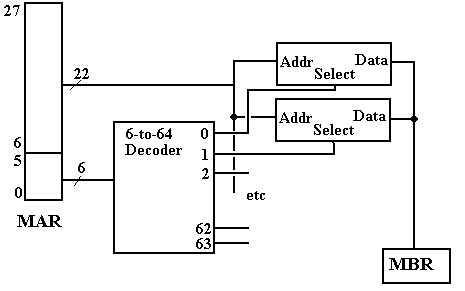
Figure: Partial Design of the Memory Unit
The high order bits of the address are received by each of the 64 4MB–chips. At any given time, only one of the 64 chips is active. If a memory read or write operation is in progress, just one of the chips will be selected, leaving the others dormant.
A Closer Examination of the Memory "Chip"
We've been able to minimise the problem of constructing a 32–to–232 decoder to that of developing a 22–to–222 decoder so far in our design. We've achieved the speed benefit that interleaving provides, but we still have the decoder issue. Now we'll look at the next step in memory design, which is the difficulty of making a 4MB chip that works.
The solution we'll utilise is to make the chip up of eight 4Mb (megabit) chips. The figures below depict the design that was used.

Figure: Eight Chips, each holding 4 megabits, making a 4MB “Chip”
Having one chip represent only one bit in the MBR has an immediate benefit. Because of the nature of chip breakdown, this is the case. If a ninth 4Mb chip is added to the mix, a basic parity memory may be created, with single bit errors being detected by circuitry (not shown) that feeds the nine bits selected into the 8-bit memory buffer register.
When we look at the decoder circuitry used in the 4Mb device, we can observe a bigger gain. It's logically equivalent to the 22–to–4194304 decoder we stated earlier, but it's made up of two 11–to–2048 decoders, which aren't hard to make.
Consider the 4Mb chip's 4194304 (222) bits as a two-dimensional array of 2048 rows (numbered 0 to 2047), each with 2048 columns (also numbered 0 to 2047). The situation is depicted in the diagram below.
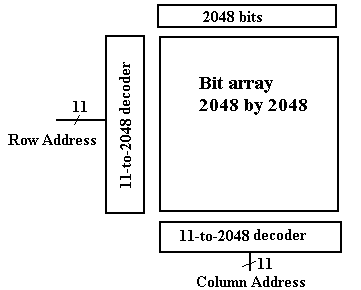
Figure: Memory with Row and Column Addresses
We now add one more feature, to be elaborated below, to our design and suddenly we have a really fast DRAM chip. For ease of chip manufacture, we split the 22-bit address into a 11-bit row address and an 11-bit column address. This allows the chip to have only 11 address pins, with two extra control (RAS and CAS – 14 total) rather than 22 address pins with an additional select (23 total). This makes the chip less expensive to manufacture.
We send the 11-bit row address first and then send the 11-bit column address. At first sight, this may seem less efficient than sending 22 bits at a time, but it allows a true speed-up. We merely add a 2048 SRAM buffer onto the chip and when a row is selected, we transfer all 2048 bits in that row to the buffer at one time. The column select then selects from this faster memory used as an on-chip buffer. Thus, our access time now has two components:
1) The time to select a new row, and
2) The time to copy a selected bit from a row in the SRAM buffer.
This design is the basis for all modern computer memory architectures.
4.4.7 SDRAM – Synchronous Dynamic Random Access Memory
As previously stated, memory's slowness in comparison to the CPU has long been a source of concern among computer designers. SDRAM – synchronous dynamic access memory – is one recent breakthrough that has been employed to overcome this problem.
Up to this point, we've just talked about standard memory types.
SRAM (Static Random Access Memory) is a type of static random access memory.
5–10 nanoseconds is a typical access time.
6 transistors were used, which was expensive and took up a lot of space.
DRAM (Dynamic Random Access Memory) is a type of random-access memory
50–70 nanoseconds is a typical access time.
One capacitor and one transistor were used to make this circuit: it was compact and inexpensive.
In a way, the desirable approach would be to make the entire memory to be SRAM. Such a memory would be about as fast as possible, but would suffer from a number of setbacks, including very large cost (given current economics a 256 MB memory might cost in excess of $20,000) and unwieldy size. The current practice, which leads to feasible designs, is to use large amounts of DRAM for memory. This leads to an obvious difficulty.
1) The access time on DRAM is almost never less than 50 nanoseconds.
2) The clock time on a moderately fast (2.5 GHz) CPU is 0.4 nanoseconds,
125 times faster than the DRAM.
The problem that arises from this speed mismatch is often called the “Von Neumann Bottleneck” – memory cannot supply the CPU at a sufficient data rate. Fortunately there have been a number of developments that have alleviated this problem. We have already discussed the idea of cache memory, in which a large memory with a 50 nanosecond access time can be coupled with a small memory with a 10 nanosecond access time and function as if it were a large memory with a 10.4 nanosecond access time. We always want faster.
The next development that we shall discuss is synchronous dynamic access memory, SDRAM for short. Although we have not mentioned it, earlier memory was asynchronous, in that the memory speed was not related to any external speed. In SDRAM, the memory is synchronized to the system bus and can deliver data at the bus speed. The earlier SDRAM chips could deliver one data item for every clock pulse; later designs called DDR SDRAM (for Double Data Rate SDRAM) can deliver two data items per clock pulse.
Modern computer designs, in an effort to avoid the Von Neumann bottleneck, use several tricks, including multi-level caches and DDR SDRAM main memory.
As an example, we quote from the Dell Dimension 4700 advertisement of July 21, 2004. The chip has two 16 KB L1 caches (an Instruction Cache and a Data Cache), 1MB L2 cache, and 512 MB of DDR SDRAM that operates with a 400 MHz bus (800 M transfers/sec) with 64 data lines – 8 bytes at a time, for a data rate of 6.4 GB/sec.
The main difference between level 1 (L1) cache and level 2 (L2) cache is that the L1 cache is on the CPU chip, while the L2 cache generally is on a different chip. For example, the IBM S390/G5 chip has 256 KB of L1 cache on the CPU chip and 4MB of L2 cache. It is likely that the existence of two (or more) levels of cache, rather than one large L1 cache, is due to two aspects of area constraints: area on the CPU chip that can be allocated to the L1 cache and the fact that larger SRAM memories tend to be slower than the smaller ones.
L1 cache memory is uniformly implemented as SRAM (Static RAM), while L2 cache memory may be either SRAM or SDRAM.
The SDRAM chip uses a number of tricks to deliver data at an acceptable rate. As an example, let’s consider a modern SDRAM chip capable of supporting a DDR data bus. In order to appreciate the SDRAM chip, we must begin with simpler chips and work up.
We begin with noting an approach that actually imposes a performance hit – address multiplexing. Consider an NTE2164, a typical 64Kb chip. With 64K of addressable units, we would expect 16 address lines, as 64K = 216. In stead we find 8 address lines and two additional control lines
 Row Address Strobe (Active Low)
 Column Address Strobe (Active Low)
This is how it goes. We structure the memory as a 256-by-256 square array, remembering that 64K = 216 = 28 • 28 = 256 • 256. Two addresses — the row address and the column address – uniquely identify each object in the memory.
The 8-bit address is interpreted in the following fashion.
 |
 | Action |
0 | 0 | An error – this had better not happen. |
0 | 1 | It is a row address (say the high order 8-bits of the 16-bit address) |
1 | 0 | It is a column address (say the low order 8-bits of the 16-bit address) |
1 | 1 | It is ignored. |
Here is that way that the NTE2164 would be addressed.
1) Assert  = 0 and place the A15 to A8 on the 8-bit address bus.
2) Assert  = 0 and place A7 to A0 on the 8-bit address bus.
For such a design, there are two design goals that are comparable.
1) The memory chip's pin count should be kept as low as possible. We have two options: 8 address pins, RAS, and CAS (10 pins) or 8 address pins, RAS, and CAS (10 pins).
There are 16 address pins in all, including an Address Valid pin (17 pins).
2) On the data bus, the number of address-related lines should be kept to a minimum.
The numbers are the same: 10 vs. 17.
We may now explore the next stage in memory speed-up with this design in mind. FPM–DRAM stands for Fast-Page Mode DRAM.
Quick-Page Mode Page mode in DRAM is an enhancement over traditional DRAM in which the row-address is fixed and data from several columns is read from the sense amplifiers. The information stored in the sense amps is organised into a "open page" that can be accessed easily. This reduces the time it takes to access the same row of the DRAM core.
The transition from FPM–DRAM to SDRAM logically entails making the DRAM interface synchronous to the data bus, with a clock signal propagated on that bus controlling it. The design problem now is figuring out how to make a memory chip that can respond quickly enough. The SDRAM core has the same fundamental design as a traditional DRAM. SDRAM sends data on one of the clock's edges, most commonly the leading edge.
Data at twice the normal rate By sending data at both edges of the clock, SDRAM (DDR–SDRAM) twice the bandwidth available from SDRAM.

Figure: DDR-SDRAM Transfers Twice as Fast
So far, we've used an SRAM memory as an L1 cache to reduce effective memory access time and Fast Page Mode DRAM to access a complete row from the DRAM chip quickly. The difficulty of making the DRAM chip faster continues to bother us. We'll have to speed up the chip a lot if we want to use it as a DDR-SDRAM.
The quantity of SRAM on a DRAM die is rising in modern DRAM designs. In most circumstances, a memory system will have at least 8KB of SRAM on each DRAM chip, allowing data to be transferred at SRAM speeds.
We now have two metrics to consider: delay and bandwidth.
The length of time it takes for the memory to produce the first element of a block is known as latency of data that is contiguous
The rate at which the memory can send data once the row address is known is known as bandwidth has been approved
Making the data bus "wider" – that is, able to transport more data bits at a time – can enhance memory bandwidth. The ideal size of the L2 cache turns out to be half the size of a cache line. So, what exactly is a cache line?
We must return to our explanation of cache memory in order to grasp the concept of a cache line. What happens if a memory read fails due to a cache miss? The byte that has been referenced must be recovered from main memory. By getting not just the required byte but also a number of neighbouring bytes, efficiency is increased.
Memory in the cache is grouped into cache lines. Assume we have an L2 cache with a 16-byte cache line size. 8-byte chunks of data would be transmitted into the L2 cache.
Let's say you need a byte with the address 0x124A and it's not in the L2 cache. The 16 bytes with addresses spanning from 0x1240 to 0x124F would be placed into a cache line in the L2 cache. This might be accomplished in two 8-byte transfers.
Assume the memory is 8-way interleaved, with chips numbered 0 through 7, with bytes 1240 and 1248 on chip 0 and 1241 and 1249 on chip 1, and so on. We also assume that each of the eight memory chips has its own set of eight data lines, resulting in a total bus width of 64 bits. The following is how we fill the cache line.
1) Assert the address on the address lines and wait for the memory delay to be calculated.
2) Use the full bus speed to transfer the first batch of 8 bytes at the same time.
3) Use the full bus speed to transfer the following batch of 8 bytes at the same time.
On each clock edge, the DDR–SDRAM would then transfer 8 bytes, for a total of 16 bytes per clock pulse. A synchronous bus running at 400 MHz would then transport data at a rate of 16 bytes per second, or 6.4 gigabits per second.
We'll wrap up this section of the debate by looking at some specifications for a memory chip that, as of July 2004, appeared to be cutting-edge. Micron DDR2 SDRAM is available in three different models.
MT46H64M4 64 MEG x 4
MT47H32M8 32 MEG x 8
MT47H16M16 16 MEG x 16
One of two bus clock periods can be used to synchronise each of these chips.
For a 200 MHz bus, this equates to 5 nanoseconds, or 400 M transfers per second in DDR.
For a 266.7 MHz bus, this translates to 3.75 nanoseconds, or 533 M transfers per second in DDR.
Each chip has 256 Mb of internal memory, which is configured as a 4-bank DRAM. This can be 4 banks of 4, 8, or 16-bit entries, depending on the chip selection. N is the number to dial. A single read or write operation on the device consists of a single 4N-bit-wide, one-clock-cycle data transfer at the DRAM core and four N-bit-wide transfers at the I/O pins.
A modern data bus might be 64 bits wide, allowing 8 bytes to be transferred at once. A bus with the above technologies would have bandwidths of either
The transport rate is 8 bytes per second.
• 400 M transfers per second = 3200 MB per second = 3.2 GB per second, or
The transport rate is 8 bytes per second.
• 533 M transfers per second = 4264 MB per second = 4.3 GB per second
4.4.9 Memory Organization in Computer Architecture
The term "memory unit" refers to a grouping of storage units or devices. The binary information is stored in bits in the memory unit. Memory/storage is generally divided into two categories:
● Volatile Memory: When the power is turned off, the data is lost.
● Non-Volatile Memory: This is a permanent storage device that does not lose data even if the power is turned off.
The access time of auxiliary memory is typically 1000 times that of main memory, putting it at the bottom of the hierarchy.
The primary memory is in the middle because it has an input/output processor (I/O) that allows it to interface directly with the CPU and auxiliary memory devices.
When the CPU requires a programme that is not in main memory, it is retrieved from auxiliary memory. Auxiliary memory is used to store programmes that are not currently in use in main memory, freeing up space in main memory for other programmes.
Program data that is currently being executed in the CPU is stored in the cache memory. The access time ratio between cache memory and main memory is roughly 1 to 710 milliseconds.

4.4.10 Memory Access Methods
Each memory type is made up of a number of different memory locations. To read data from any memory, you must first locate it, and then read the data from that location. The methods for retrieving data from memory locations are as follows:
- Random Access: Main memories are random access memories with a unique address for each memory location. Any memory location in any sequence can be reached in the same amount of time using this unique address.
- Sequential Access: This approach allows you to access memory in a sequential or sequential order.
- Direct Access: Information is stored in tracks in this manner, with each track having its own read/write head.
4.5.1 Memory and I/O Interfacing
A CPU is coupled to several memory chips and I/O devices.
A schematic diagram for connecting memory chips and I/O devices to a CPU is shown in the diagram below.
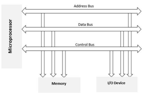
Memory Interfacing
The microprocessor sends out the address of a memory region or an I/O device when we execute any instruction. A decoding circuit selects the appropriate memory chip or I/O device.
Memory requires some signals to read from and write to registers, while the microprocessor sends out signals to read and write data.
The memory requirements must be matched with the microprocessor signals during the interfacing process. As a result, the interfacing circuit should be constructed to match the memory signal needs with the signals of the CPU.
I/O interfacing
As we all know, the keyboard and displays are utilised to communicate with the rest of the world. As a result, we must link the keyboard and displays with the microprocessor. This is referred to as I/O interfacing. We use latches and buffers to connect the keyboards and displays to the microprocessor for this form of interface.
The fundamental disadvantage of this interface, however, is that the microprocessor can only execute one function.
4.5.2 8279 Programmable Keyboard
The Intel 8279 is a keyboard interface device that can be programmed. Microprocessor kits and microprocessor-based systems include data input and display as standard features.
The 8279 was created to work with Intel's 8-bit microprocessors.
The 8279 is divided into two sections: the keyboard and the display.
The keyboard section's job is to connect the keyboard to the CPU, which serves as an input device. It can also be used to connect to toggle or thumb switches.
The display section's purpose is to power alphanumeric displays or indication lights. The microprocessor bus is directly attached to it.
The microprocessor is no longer required to scan the keyboard or update the display.
Some important Features are:
1. Multiple keyboard display activities at the same time
2. Mode of the scanned sensor
3. Scanned keyboard mode is the third option.
4. FIFO keyboard with 8 characters
5. Input mode with strobes
6. Contact debounce with 2-key lock out or N-key roll ove
7. Display with a single 16-character lin
8. Numerical display with dual 8 or 16 digit
9. Disrupt output when a key is pressed
10. From the CPU, you can programme scan timing and mode.
4.5.3 8257 DMA Controller
The accumulator is used to transport data from fast I/O devices to the memory or from the memory to I/O devices. The Direct Memory Access (DMA) approach is favoured in this case. Data is transmitted directly from an I/O device to RAM or from RAM to an I/O device in the DMA data transfer mechanism.
The device requests that the CPU maintain its address, data, and control buses using a DMA controller, allowing it to move data directly to and from memory. Only after receiving the HLDA signal from the CPU is the DMA data transmission started.
How DMA operations are performed?
The operations that a DMA does are as follows:
o To transport data between the device and the memory, the device must first send a DMA request (DRQ) to the DMA controller.
o The DMA controller sends the CPU a Hold Request (HRQ) and waits for the HLDA.
o When the CPU receives the HLDA signal, it relinquishes control of the bus and responds to the HOLD request through the HLDA signal.
o Now that the CPU is in the HOLD state, the DMA controller must manage the operations between the CPU, memory, and I/O devices through the buses.
4.5.4 Intel 8257
0 The Intel 8257 is a DMA controller that may be programmed.
o It's a programmable Direct Memory Access (DMA) controller with four channels.
o It's a 40-pin I.C. Package that requires a +5V supply to work.
o It is capable of three operations: read, write, and verify.
o Each channel has two 16-bit registers: the DMA address register and the byte counter register.
Each channel has a 64kb data transfer capacity and can be set independently.
o It has two modes of operation: Master and Slave.
Architecture 4.5.5 8257
The Intel 8257's architecture is depicted in the graphic below:
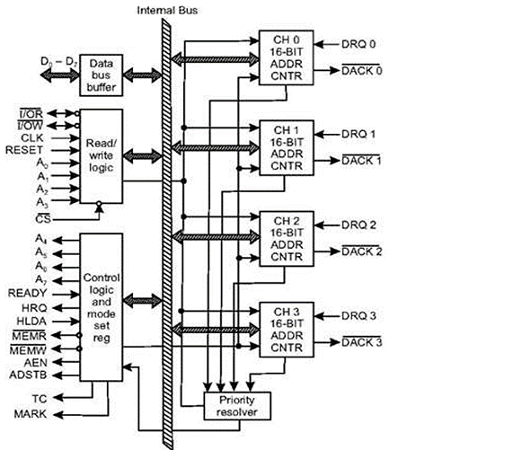
4.5.6 8257 Pin Description
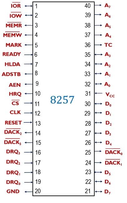
DRQ0 - DRQ3: DMA request lines are what they're called. The DMA request is sent on one of these lines by an I/O device. A HIGH condition on the line triggers a DMA request.
DACK0 - DACK3: DMA acknowledgment lines are what they're called. One of these lines is used by the Intel 8257 to transmit an acknowledge signal to an I/O device, telling it that it has been selected for DMA data transmission. A LOW recognises the I/O device on the line.
A0 - A7: These are the lines for addressing people. Lines A0 - A3 are bidirectional. The 8257 in master mode generates four LSBs of 16-bit memory addresses on these lines. These lines are all the input lines in slave mode. One of the registers to be read or programmed is selected by the inputs. In master mode, the A4 - A7 lines create tristated outputs that carry 4 through 7 of the 16-bit memory address created by the Intel 8257.
This is a series of data lines, D0 through D7. These are bidirectional lines with three states. During controller programming, the CPU uses these data lines to send data to the DMA address register, the byte count register, and the mode set register.
AEN: Enable the address latch.
A HIGH on this line locks the 8MSBs of the address sent on the D-bus into the Intel 8212 attached for this purpose.
CS: It's a chip pick option.
I/O read (I/OR). It is a two-way street. During the DMA write cycle, it is used to read data from the I/O device in output mode.
(I/OW): (I/O) (I/O) (I/O) (I/O) (I/ It is a two-way street. During the DMA read cycle, it permits data to be transferred to the I/O device in output mode. Data is moved from the memory to the hard drive.
MEMR stands for "memory read."
MEMW stands for Memory Erase Memory Write.
Byte Count (TC) is a term that refers to the number of bytes (Terminal count).
MODULO 128 MARK MODULO 128 MARK MODULO 128 MARK MODULO 128 M
CLK stands for Clock.
Hold request (HRQ)
Hold acknowledge (HLDA)
4.5.7 Microprocessor - I/O Interfacing Overview
We'll talk about memory and IO interfacing with the 8085 in this chapter.
The communication path between two components is known as the interface. Memory interfacing and I/O interfacing are the two forms of interfacing.
Block Diagram of Memory and I/O Interfacing
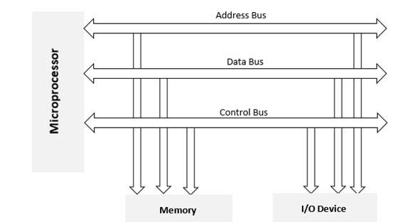
8085 Interfacing Pins
The list of 8085 pins utilised for interacting with other devices is as follows:
A15 - A8 are the first five letters of the alphabet (Higher Address Bus)
2. Lower Address/Data Bus (AD7 - AD0)
3. A.L.E.
RD is number four.
WR No. 5
6. GETTING READY
Ways of Communication − Microprocessor with the Outside World?
There are two methods through which the microprocessor can communicate with the outside world.
Serial Communication Interface (SCI) and Parallel Communication Interface (PCI) are two types of communication interfaces.
Serial Communication Interface - In this method of communication, the interface receives a single byte of data from the CPU and serially transmits it to the other system.
Parallel Communication Interface − The interface receives a byte of data from the microprocessor and transfers it bit by bit to the other systems in a parallel (or simultaneous) method, and vice versa.
4.5.8 External memory interfacing in 8085: RAM and ROM
We've spoken about how the 8085 reads and writes data from and to memory several times in this 8085 course. However, unlike microcontrollers, which have some built-in memory, microprocessors, with the exception of a few registers, do not have their own memory. So, where does 8085 get its data from and write it to?
We'll need to use external memory chips because the 8085 doesn't have much internal memory.
Memory support in 8085
The address bus of an 8085 microprocessor is 16 bits. Each bit can accept one of two values: 0 or 1. So, on a 16-bit address bus, the maximum number of addresses that may be created is 256. And each distinct address relates to a memory block of 8 bits or 1 byte in size.

As a result, we can state that the 8085 can support memory chips up to 64 kB in size. We can also interconnect a memory chip with a smaller size. We can also connect multiple memory chips to a single 8085 CPU as long as their total size does not exceed 64 kB. Let's figure out how to accomplish all of this.
4.5.9 Memory interfacing – Problem statement
Interface a 1kB EPROM and a 2 kB RAM with microprocessor 8085. The address allotted to 1 kB EPROM should be 2000H to 22FFH. You can assign the address range of your choice to the 2 kB RAM.
Understanding the pins of the specified memory chips is the first step in solving this challenge.
Pin diagram of memory chips
Except for the WR pin, which is present in RAM but not in a ROM, RAM and ROM have the identical pins. Let's take a look at the pins one by one.
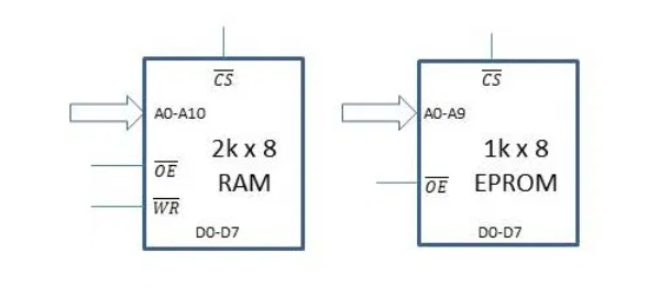
Data pins: Because each memory location contains eight bits, the memory chip has eight data lines D0-D7 attached to it.
Address pins: The number of address pins depends on the size of the memory. In this case, a memory of size 1 kB x 8 will have 210 different memory locations. Hence, it will have ten address lines A0 to A9. Similarly, the 2 kB RAM will have 211 different memory locations. So, there are 11 address lines A0-A10.
CS pin: When this pin is enabled, the memory chip recognises that the CPU is attempting to communicate with it and responds appropriately. This signal must be generated for each chip based on the range of addresses assigned to them. Essentially, we choose a chip only when it is required. This is done through the Chip Select (CS) pin.
OE pin: The memory chip can output data onto the data bus when this active-low output enable pin is enabled.
WR pin: When this active-low memory write pin is activated, data from the data bus is written to the memory chip at the address bus's defined location.
VCC and GND pins: These pins are used to power the integrated circuits. These pins will not be shown in the diagram for clarity.
In 8085, there are three different types of buses: address buses, data buses, and control buses. The memory chip will be attached to each of these buses.
4.5.10 Connecting Control Signals
In the memory chips, there are two pins for control signals – OE (Output Enable) and WR (Memory Write). These will be connected to the control signals generated using a 3 to 8 decoder. To read about the generation of control signals, you can read our post on Demultiplexing of Bus and Generating Control Signals. The circuit for generating control signals is shown below.

Four control signals are generated when we input the WR, RD and IO/M signals from the 8085 to the 3:8 decoder – IOR, IOW, MEMR and MEMW. Since we are dealing with memory, we will just need MEMR and MEMW signals.
While reading from a memory chip, it’s output should be enabled. So, MEMR will be connected to the OE pin. Similarly, for writing to a memory chip, MEMW will be connected to the WR pin of the RAM. After completing these two connections, we are done with the control signals except CS. We will deal with that in a bit.
Data Bus interfacing
There are eight lines comprising the data bus of both 8085 and the memory chips. The interfacing of the data bus is the simplest part. We just connect corresponding lines (D0-D7 from 8085) to the corresponding pins (D0-D7 of the memory chip).
Address bus Interfacing
A 2kB RAM with 11 address lines is available. As a result, the first 11 lines of the 8085's address bus will be connected to the 2kB RAM's corresponding address lines. Similarly, the first 10 lines of the 8085's address bus will be connected to the 1kB EPROM's equivalent lines. The chip select (CS) signal will be generated using the remaining address lines.
Generating the chip select signal
This is a little tough, but it's the most crucial component of the solution. Let's take it one step at a time to get a sense of how to generate the chip select signal for a memory with a certain size and address range.
Let's make a list of the 1kB EPROM's starting and ending addresses.
The most significant bit is A15, and the least significant bit is A0. The EPROM can be placed anywhere between 2000H to 22FFH (as given in the question.) To convert them to binary, follow these steps:
2000H = 0011 0000 0000 0000
22FFH = 0011 0011 1111 1111
Address bit number | A15 | A14 | A13 | A12 | A11 | A10 | A9 | A8 | A7 | A6 | A5 | A4 | A3 | A2 | A1 | A0 |
Starting address | 0 | 0 | 1 | 1 | 0 | 0 | 0 | 0 | 0 | 0 | 0 | 0 | 0 | 0 | 0 | 0 |
Ending Address | 0 | 0 | 1 | 1 | 0 | 0 | 1 | 1 | 1 | 1 | 1 | 1 | 1 | 1 | 1 | 1 |
From the above table, we can observe that ten bits from A0 to A9 are changing. These ten bits are directly connected to the address lines of the memory chip.
These ten bits take the value of either 0 or 1 to form addresses. The first address is 00 0000 0000, and the second address is 00 0000 0001, the third is 00 0000 0010 and so on. The last address will be 11 1111 1111.
Meanwhile, bits A11 to A15 remain unchanged and have no impact on the memory chip's addressing mechanism. As a result, we can deduce that the values of bits A15-A11 (0011 00) in the preceding table are unique and unchangeable for this memory chip. The address will not correspond to this memory chip if even one of these bits changes. As a result, we can utilise the A15-A11 values to uniquely identify this memory chip, which is exactly what the CS signal is designed to do.
We can say that when A15 = A14 = A11 = A10 = 0 and A13 = A12 = 1, then our memory chip should be selected. Now, we need to design the logic to generate the CS signal. The resulting Boolean equation of CS will be:
CS = Complement of (A15* . A14* . A13 . A12 . A11* . A10*)
This equation can be implemented using NAND Gate. The final chip select logic for 1kB EPROM is illustrated below.

We must now create a chip select signal for the second memory chip, which is a 2kB RAM chip. The procedure is very similar to the last one, however it differs in two ways:
The amount of RAM available varies. As a result, instead of 10, there are 11 address lines.
We don't have an address range to work with here. We are given the freedom to make our own decisions.
We connect the first 11 address lines of the 8085 microprocessor to the 11 address lines of the 2kB RAM, just as we did in the prior scenario. These bits will generate 2 * 1024 distinct addresses based on their values of 0 and 1. From 000 0000 0000 to 111 1111 1111, the address bits A10-A0 will vary.
What about the address bits that are left? They don't play a part in addressing the memory in this 2kB RAM, though. As a result, we can set them to a certain value without impacting anything else. Let's make them 0000 0. As a result, the chip's address range is 0000 0000 0000 0000 through 0000 0111 1111 1111. The address range will be 0000H to 07FFH in hexadecimal.
Address bit number | A15 | A14 | A13 | A12 | A11 | A10 | A9 | A8 | A7 | A6 | A5 | A4 | A3 | A2 | A1 | A0 |
Starting address | 0 | 0 | 0 | 0 | 0 | 0 | 0 | 0 | 0 | 0 | 0 | 0 | 0 | 0 | 0 | 0 |
Ending Address | 0 | 0 | 0 | 0 | 0 | 1 | 1 | 1 | 1 | 1 | 1 | 1 | 1 | 1 | 1 | 1 |
Here, we utilise a similar method. The remaining bits A15-A11 are used to form a chip select signal that uniquely identifies this chip. CS = Complement of (A15*. A14*. A13*. A12*. A11*) will be the boolean equation.
The following figure shows how to execute this equation using a NAND Gate to generate the CS signal.

4.5.11 The final circuit
It's time to finish the circuit now that we have the chip choose logic and have agreed on all of the connections. The entire external memory interface circuit can be divided into five sections:
Microprocessor 8085
Address/data bus demultiplexing
Control signals are generated.
Chip select signals are generated.
Chips for memory
The complete circuit with all five pieces indicated above merged into a single circuit is shown in the photographs below. In the first diagram, only the connections are depicted. The circuit's many subsections are labelled in the schematic that follows.
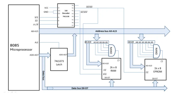
The technique of connecting the external memory to the 8085 CPU is depicted in the diagram above. If you have any questions on the topic, please leave a comment below and we will respond as soon as possible.
4.6.1 Introduction:
A memory map is a large table, essentially a database, that contains all of the information on how a computer system's memory is organised. A memory map functions similarly to a massive office organiser. Each computer file in the map has its own unique memory location, ensuring that no other data can accidentally overwrite or destroy it.
A computer's operating system (OS) must constantly be able to access the relevant areas of its memory at the correct moments in order for it to work effectively. The memory map tells the operating system how much memory is available when a computer initially boots up (starts). The memory map ensures that data is always written to and read from the correct locations as the machine runs. The memory map also ensures that debuggers on the computer may map memory locations to actual data.
The OS might (and presumably would) write data to and read data from the wrong places if there was no memory map or if an existing memory map became corrupted. As a result, when data was read, it didn't always correspond to the correct files or programmes. The problem would most likely begin tiny and undetectable, increase over time, and only become apparent after significant damage to stored data and programmes had occurred. In the end, some or all of the apps might fail to execute, resulting in the loss of numerous vital data files.
4.6.2 Overview of Memory-Mapping
What Is Memory-Mapping?
Memory-mapping is a technique for mapping a section of a file on disc to a range of addresses within an application's address space. After that, the application may access files on disc in the same way that it can access dynamic memory. When compared to utilising functions like fread and fwrite, this speeds up file reads and writes.
Benefits of Memory-Mapping
Efficiency, faster file access, the ability to share memory between applications, and more efficient coding are the main advantages of memory-mapping.
Faster File Access
Using memory maps to access files is faster than using I/O operations like fread and fwrite. Rather of allocating, copying into, and subsequently deallocating data buffers held by the process, data is read and written utilising the operating system's virtual memory capabilities.
When the map is originally created, MATLAB® does not access data from the disc. When a certain part of the memory map is accessed, it only reads or writes the file on disc, and it only reads that specific area. This allows for speedier access to the mapped data at random.
Efficiency
Data in a file can be accessed as if it had been read into an array in the application's address space when a file is mapped into memory. MATLAB just allocates address space for the array at first; it does not read data from the file until the mapped region is accessed. As a result, memory-mapped files allow applications to access data segments in extraordinarily large files without having to first read the full file into memory.
Efficient Coding Style
Memory-mapping allows you to access file data using regular MATLAB indexing procedures in your MATLAB application. You can read the contents of a file that has been mapped to memory using the same MATLAB statements that you used to read variables from the MATLAB workspace. In the presently active workspace, the contents of the mapped file show as an array. To read or write data from the file, you just index into this array. As a result, you don't need to invoke the fread and fwrite functions explicitly.
If y is the data to be written to a file and x is a memory-mapped variable in MATLAB, then writing to the file is as simple as
x.Data = y;
Sharing Memory Between Applications
As demonstrated in the diagram below, memory-mapped files can also be used to share data between apps. This is accomplished by mapping chunks of the same file to each programme. This function can be used to move big data sets between MATLAB and other programmes.
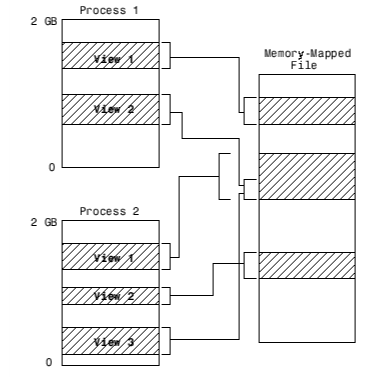
When to Use Memory-Mapping
The amount of benefit you gain from mapping a file to memory is mostly determined on the file's size and format, the manner data in the file is used, and the computer platform you're using.
When Memory-Mapping Is Most Useful
Memory-mapping is most effective with binary files and in the following situations:
1. If you have a huge file that you wish to access one or more times at random.
2. For short files that you only want to read once and then access regularl
3. For data that you'd like to share between different apps
4. Working with data in a file as if it were a MATLAB array
When the Advantage Is Less Significant
Memory-mapping benefits are not completely utilised in the following sorts of files:
Memory-mapping is not possible with formatted binary files like HDF or TIFF, which require specialised readers. It can be difficult to describe the information included in these files. You can't directly retrieve data from the mapped segment; instead, you must create arrays to retain the data.
For the data in text or ASCII files to be meaningful, you must transform the text in the mapped region to an appropriate type. This necessitates the use of more address space.
Larger files over a few hundred megabytes take a significant amount of the virtual address space required by MATLAB to process your programme. When working with large mapping files, MATLAB may display more out-of-memory issues. If MATLAB has been running for a while, or if the memory used by MATLAB becomes fragmented, this is more likely.
Maximum Size of a Memory Map
The maximum amount of data you can map with a single instance of a memory map is 2 gigabytes on 32-bit computers and 256 terabytes on 64-bit platforms due to operating system and MATLAB constraints. If you need to map more than this, you can either make additional maps for different parts of the file or shift the window of a single map to different parts of the file.
Byte Ordering
Memory-mapping only works with data that has the same byte ordering scheme as your operating system's native byte ordering. Data written on a Linux system, for example, can be read on a Windows system since both Linus Torvalds' Linux® and Microsoft® Windows® systems employ little-endian byte ordering. You can use the computer function to find out what your current system's native byte ordering is.
4.6.3 Memory Mapping
The map() system call offers mapping in the caller process's virtual address space, which maps files or devices into memory. There are two forms of this.
● File mapping or File-backed mapping – This mapping connects the virtual memory of the process to the files. This indicates that reading or writing to those memory locations causes the file to be read or written. The default mapping type is this.
● Anonymous mapping – This mapping, which is not backed by any file, maps the area of the process' virtual memory. The value of the contents is set to zero. This mapping is comparable to dynamic memory allocation (malloc()) and is utilised for certain allocations in some malloc() implementations.
● Memory from one process mapping may be shared with other processes' mappings. When two processes map the same section of a file, they share the same pages of physical memory in one of two ways.
● When a child process is established, it inherits the mappings of the parent process, and these mappings relate to the same physical memory pages as the parent process. Different pages for the child process would be created whenever the data in the child process changed.
● Depending on the mapping type, each process can view changes to the page contents made by other processes when two or more processes share the same pages. There are two types of mappings: private and shared.
● Private Mapping (MAP_PRIVATE) – Other processes are not aware of changes to the contents of this mapping, and the mapping is not saved to the underlying file.
● Shared Mapping (MAP_SHARED) − Other processes can see changes to the contents of this mapping, and the mapping is saved to the underlying file.
#include <sys/mman.h>
Void *mmap(void *addr, size_t length, int prot, int flags, int fd, off_t offset);
On success, the above system call delivers the mapping's starting address; on failure, it returns MAP FAILED.
The virtual address addr can be supplied by the user or created automatically by the kernel (upon passing addr as NULL). The specified field length necessitates the mapping size in bytes. PROT NONE, PROT READ, PROT WRITE, PROT EXEC are memory protection values that denote regions that cannot be accessed, read, written, or executed, respectively. This value can be a single value (PROT NONE) or a combination of the three flags (ORd) (last 3). MAP PRIVATE or MAP SHARED are the mapping types indicated by the field flags. The column ‘fd' denotes the file descriptor that identifies the file to be mapped, and the field ‘offset' denotes the file's beginning point; if the entire file is to be mapped, offset should be zero.
#include <sys/mman.h>
Int munmap(void *addr, size_t length);
If the system call succeeds, it returns 0; if it fails, it returns -1.
Munmap is a system call that executes the unmapping of a previously memory mapped region. The fields addr and length specify the initial address of the mapping and the size in bytes of the mapping to be unmapped, respectively. The mapping and unmapping would normally be done for the entire mapped region. If this has to be different, it should be shrunk or cut into two pieces. This call has no effect if the address has no mappings, in which case it returns 0. (success).
Consider the following scenario:
Step 1 − Write into file Alpha Numeric characters as shown below –
0 | 1 | 2 | … | 25 | 26 | 27 | 28 | 29 | 30 | 31 | 32 | 33 | 34 | 35 | 36 | 37 | 38 | … | 59 | 60 | 61 |
A | B | C | … | Z | 0 | 1 | 2 | 3 | 4 | 5 | 6 | 7 | 8 | 9 | A | b | c | … | x | y | z |
Step 2 – The mmap() system call is used to map the contents of a file into memory. After mapping into memory, this would return the initial address.
Step 3 – Because it avoids utilising the expensive read() system function, you can access the file contents using array notation (or pointer notation). Avoid numerous copies between user space, kernel space buffers, and the buffer cache by using memory mapping.
Step 4 – Continue reading the contents of the file until the user inputs “-1.” (signifies end of access).
Step 5 − Clean-up tasks include unmapping the mapped memory region (munmap()), closing the file, and deleting it.
/* Filename: mmap_test.c */
#include <stdio.h>
#include <sys/stat.h>
#include <sys/types.h>
#include <fcntl.h>
#include <unistd.h>
#include <stdlib.h>
#include <sys/mman.h>
Void write_mmap_sample_data();
Int main() {
Struct stat mmapstat;
Char *data;
Int minbyteindex;
Int maxbyteindex;
Int offset;
Int fd;
Int unmapstatus;
Write_mmap_sample_data();
If (stat("MMAP_DATA.txt", &mmapstat) == -1) {
Perror("stat failure");
Return 1;
}
If ((fd = open("MMAP_DATA.txt", O_RDONLY)) == -1) {
Perror("open failure");
Return 1;
}
Data = mmap((caddr_t)0, mmapstat.st_size, PROT_READ, MAP_SHARED, fd, 0);
If (data == (caddr_t)(-1)) {
Perror("mmap failure");
Return 1;
}
Minbyteindex = 0;
Maxbyteindex = mmapstat.st_size - 1;
Do {
Printf("Enter -1 to quit or ");
Printf("enter a number between %d and %d: ", minbyteindex, maxbyteindex);
Scanf("%d",&offset);
If ( (offset >= 0) && (offset <= maxbyteindex) )
Printf("Received char at %d is %c\n", offset, data[offset]);
Else if (offset != -1)
Printf("Received invalid index %d\n", offset);
} while (offset != -1);
Unmapstatus = munmap(data, mmapstat.st_size);
If (unmapstatus == -1) {
Perror("munmap failure");
Return 1;
}
Close(fd);
System("rm -f MMAP_DATA.txt");
Return 0;
}
Void write_mmap_sample_data() {
Int fd;
Char ch;
Struct stat textfilestat;
Fd = open("MMAP_DATA.txt", O_CREAT|O_TRUNC|O_WRONLY, 0666);
If (fd == -1) {
Perror("File open error ");
Return;
}
// Write A to Z
Ch = 'A';
While (ch <= 'Z') {
Write(fd, &ch, sizeof(ch));
Ch++;
}
// Write 0 to 9
Ch = '0';
While (ch <= '9') {
Write(fd, &ch, sizeof(ch));
Ch++;
}
// Write a to z
Ch = 'a';
While (ch <= 'z') {
Write(fd, &ch, sizeof(ch));
Ch++;
}
Close(fd);
Return;
}
Output
Enter -1 to quit or enter a number between 0 and 61: 3
Received char at 3 is D
Enter -1 to quit or enter a number between 0 and 61: 28
Received char at 28 is 2
Enter -1 to quit or enter a number between 0 and 61: 38
Received char at 38 is c
Enter -1 to quit or enter a number between 0 and 61: 59
Received char at 59 is x
Enter -1 to quit or enter a number between 0 and 61: 65
Received invalid index 65
Enter -1 to quit or enter a number between 0 and 61: -99
Received invalid index -99
Enter -1 to quit or enter a number between 0 and 61: -1
4.7.1 Serial in Serial Out (SISO) Shift Register
Serial In Serial Out (SISO) shift registers are a type of shift register in which data is loaded and retrieved from the shift register in serial mode. Figure depicts an n-bit synchronous SISO shift register that is responsive to the clock pulse's positive edge. At the input of the first flip-flop, the data word to be stored is fed bit by bit. Furthermore, all other flip-flops' inputs (save the first, FF1) are driven by the outputs of the ones before them, for example, the input of FF2 is controlled by the output of FF1. Finally, the data saved in the register is serially accessed at the output pin of the nth flip-flop.

Initially, all of the register's flip-flops are cleared by applying a high voltage to their clear pins. Following that, the input data word is serially supplied to FF1.
As soon as the first leading edge of the clock emerges, the bit occurring at the D1 pin (B1) is stored into FF1. B1 is saved in FF2 during the second clock tick, while a new bit is entered into FF1 (B2).
Every rising edge of the clock pulse causes a similar shift in data bits. This means that the data in the register shifts one bit to the right for every single clock pulse. As a result, the design in Figure is known as a right-shift SISO shift register. The first bit of an input word appears at the output of the nth flip-flop for the nth clock tick after the data transfer has been explained. When more clock cycles are applied, the serial output is the next set of bits from the input data word (Table). Figure depicts the waveforms related to the same.
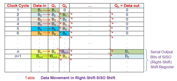
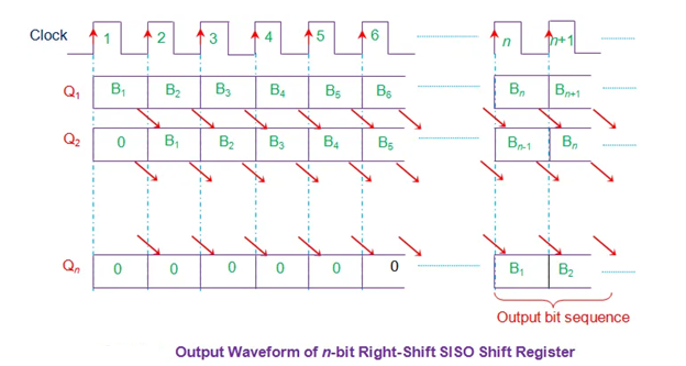
A left-shift SISO shift-register can exist in the same way as the right-shift SISO shift-register depicted. The operating idea stays the same, with the exception that data will be moved from right to left.

4.7.2 Shift Registers: Serial-in, Serial-out
For each stage, serial-in, serial-out shift registers delay data by one clock time.
Each register will have a bit of data stored in it. The length of a serial-in, serial-out shift register can range from one to 64 bits, with higher lengths possible when registers or packages are cascaded.
A single stage shift register receiving data that isn't synced with the register clock is shown below.
When the clock goes from low to high, the “data in” at the D pin of the type D FF (Flip-Flop) does not change levels.
To improve the reliability of a digital logic circuit, we may want to synchronise the data to a system-wide clock in the circuit board.

The apparent point (as shown in the diagram below) is that whatever "data in" is present at a type D FF's D pin is transferred from D to output Q at clock time.
Because our example shift register contains positive edge sensitive storage elements, as the clock transitions from low to high, the output Q follows the D input, as represented by the up arrows in the diagram above.
Because the data is stable well before and after the clock edge, it is clear what logic level is present at clock time.
In multi-stage shift registers, this is almost never the case. However, this was a simple example to begin with. We're just interested in the positive clock edge, which runs from low to high.
It is possible to disregard the dropping edge. At the clock time above, it is quite apparent to notice Q following D.
In the diagram below, the "data in" appears to change as the positive clock edge approaches.
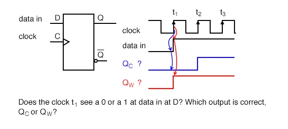
What does the type D FF observe at clock time? Since “data in” appears to change at clock time t1 above, what does the type D FF observe at clock time?
The short, simplistic explanation is that it sees the data that was present at D before the clock started ticking.
At clock time t1, that is what is transferred to Q. QC is the proper waveform. If Q is not already zero at t1, it will be at t2.
Until time t2, when Q climbs high, the D register does not see a one.

Since data, above, present at D is clocked to Q at clock time, and Q cannot change until the next clock time, the D FF delays data by one clock period, provided that the data is already synchronized to the clock. With a one-clock-period delay, the QA waveform is the same as "data in."
Following is a more thorough look at what the type D Flip-input Flop's sees at clock time.
Take a look at the diagram below. We need more information to figure out what the D FF sees because “data in” appears to alter at clock time (above).
We can infer certain conclusions based on data sheet information if the "data in" comes from another shift register stage of the same kind D FF.
Data sheets, which were previously only available in a collection called a data book, are used by manufacturers of digital logic to provide information on their parts.
Although data booklets are still available, the manufacturer's website is the most up-to-date source.
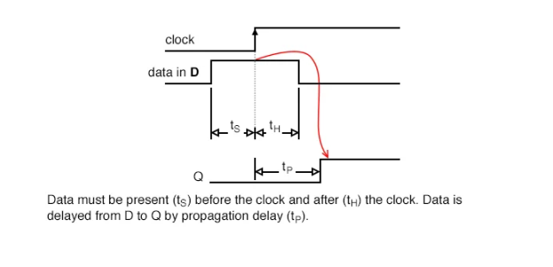
The following data was extracted from the CD4006b data sheet for operation at 5VDC, which serves as an example to illustrate timing. [*]
● tS=100ns
● tH=60ns
● tP=200-400ns typ/max
The setup time is tS, and the time data must exist before the clock time. Data must be present at D 100ns before the clock in this example.
Furthermore, after the clock time, the data must be held for a hold time of tH=60ns. To reliably clock data from D to Q of the Flip-Flop, these two requirements must be met.
If the data at D comes from another shift register stage, meeting the setup time of 60ns is not an issue because it has been there for the entire preceding clock period.
A clock frequency of 1 Mhz, for example, has a clock period of 1000 seconds, which is plenty of time.
Data will be present for 1000s prior to the clock, which is far longer than the needed tS of 60ns.
Because D coupled to Q of another stage cannot change faster than the propagation delay of the preceding stage, tP=200ns, the hold time tH=60ns is reached.
As long as the propagation delay of the previous D FF is longer than the hold time, the hold time is reached.
For the CD4006b, data at D pushed by another stage Q will not change faster than 200ns.
To recapitulate, if Flip-Flops are cascaded into a multi-stage shift register, output Q follows input D at virtually clock time.
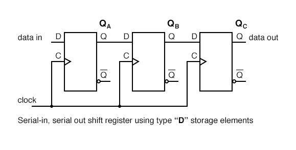
To build a three-stage shift register, three type D Flip-Flops are cascaded Q to D and the clocks paralleled.

To create an alternate variant of the shift register above, Type JK Flip Flops were cascaded Q to J, Q' to K with clocks in parallel.
The last stage of a serial-in/serial-out shift register has a clock input, a data input, and a data output.
The other stage results are generally unavailable. It would be a serial-in, parallel-out shift register otherwise.
The waveforms below can be used with either of the two variants of the serial-in, serial-out shift register described above.
A three-stage shift register temporarily stores 3-bits of data and delays it by three clock cycles from input to output, as seen by the three pairs of arrows.
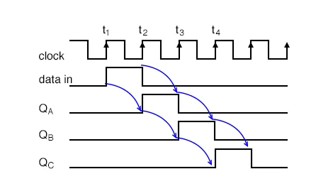
A “data in” of 0 is clocked from D to Q of all three stages at clock time t1. D of step A, in particular, notices a logic 0, which is timed to QA and remains there until time t2.
A “data in” of 1 is timed from D to QA at clock time t2. A 0 from the preceding stages is timed to QB and QC at stages B and C.
A “data in” of 0 is clocked from D to QA at clock time t3. Due to “data in” being zero, QA becomes low and stays low for the remaining clocks. Due to a 1 from the previous round, QB goes high at t3. Due to a low from the previous stage, QC is still low after t3.
Due to the high feed to D from the previous stage QB, QC finally goes high at clock t4. 0s have been shifted into all previous stages. All logic 1s will have been moved out, replaced by 0s, after the next clock pulse at t5.
4.7.3 Serial-in/serial-out devices:
We'll take a closer look at the following parts from Texas Instruments that are available as integrated circuits.
Follow the links for complete device info sheets.
18-bit serial-in/ serial-out shift register CD4006b
64-bit serial-in/ serial-out shift register CD4031b
Dual 64-bit serial-in/ serial-out shift register CD4517b
The following serial-in/ serial-out shift registers are 4000 series CMOS (Complementary Metal Oxide Semiconductor) family parts.
As a result, they'll work with a 3- to 15-volt VDD positive power source. The VSS pin is connected to the ground.
The shift clock's highest frequency, which fluctuates with VDD, is a few megahertz.

The 18-bit CD4006b has two stages of 4-bits and two more stages of 5-bits, as well as a 4-bit output tap.
As a result, the 5-bit stages can function as 4-bit shift registers.
The output of one shift register must be cascaded to the input of another, and so on, until all stages generate a single shift register, as shown below.
Below is a picture of a CD4031 64-bit serial-in/ serial-out shift register.
There are a few pins that aren't connected (nc). From the 64th stage, Q64 and Q'64, both Q and Q' are available.
There is also a Q64 that is “delayed” by half a clock cycle from a half stage. A data selector, located near the shift register's data input, is a key feature.
The "mode control" alternates between data 1 and data 2. If “mode control” is set to high, data from “data 2” will be picked for input to the shift register.
When the “mode control” is logic low, the “data 1” option is chosen. The two diagrams below provide examples of this.
The “data 2” above is connected to the shift register's Q64 output. The Q64 output is sent back to the shifter data input D when “mode control” is set to high.
Data will flow back and forth from the output to the input. As illustrated above, the data will repeat every 64 clock pulses.
The question is how this data pattern ended up in the shift register in the first place.

The CD4031 "data 1" is picked for input to the shifter when "mode control" is set to low.
Because the lower data selector gate is deactivated, the output, Q64, is not recirculated.
By disabled, we mean that the lower NAND gate's logic low "mode select" inverted twice to a low prohibits any signal on the lower pin (data 2) from reaching the gate output.
As a result, it is deactivated.
Above is a CD4517b dual 64-bit shift register. The taps at the 16th, 32nd, and 48th stages should be noted.
That means that one of the 64-bit shifters can be used to configure shift registers of those widths.
Of course, the 64-bit shifters can be cascaded to make a shift register with 80, 96, 112, or 128 bits.
When cascading the two shifters, the clocks CLA and CLB must be paralleled. For routine shifting operations, WEB and WEB are grounded.
DA and DB are the data inputs to shift registers A and B, respectively.
Let's say we need a 16-bit shift register.
Is it possible to set this up with the CD4517b? Why not make a 64-shift register out of the same component?
For section B, we have a CD4517b wired as a 16-bit shift register.
CLB is the section B clock. CLB is the time stamp for the data. And the data that has been delayed by 16 clocks is taken from Q16B. The write enable, WEB, is anchored.
For the independent section A, we demonstrate the identical CD4517b wired as a 64-bit shift register.
The section A clock is CLA. CLA is where the data is entered. Q64A collects data that has been delayed by 64-clock pulses. Section A's write enable, WEA, is grounded.
Applications of shift Registers –
1. Shift registers are used to store temporary data.
2. Data transport and manipulation are also done with shift registers.
3. To add time delay to digital circuits, serial-in serial-out and parallel-in parallel-out shift registers are utilised.
4. The serial-in parallel-out shift register is employed in communication lines where demultiplexing of a data line into numerous parallel lines is necessary.
5. To convert parallel data to serial data, a Parallel in Serial out shift register is utilised.
4.8.1 Shift Registers: Serial-in, Parallel-out (SIPO) Conversion
A serial-in, parallel-out shift register is similar to the serial-in, serial-out shift register in that it shifts data into internal storage elements and shifts data out at the serial-out, data-out, pin.
It is different in that it makes all the internal stages available as outputs. Therefore, a serial-in, parallel-out shift register converts data from serial format to parallel format.
An Example of Using Serial-in, Parallel-out Shift Register
After the fourth clock pulse, four data bits are shifted in by four clock pulses over a single wire at data-in, and the data is available concurrently on the four Outputs QA to QD.
The serial-in, parallel-out shift register's practical application is to transfer data from serial format on a single wire to parallel format on several wires.
Let's use the four outputs to light up four LEDs (light emitting diodes). (QA QB QC QD ).
The serial-in, parallel-out shift register's details are quite straightforward. It has the appearance of a serial-in, serial-out shift register with taps on each stage output.
At SI, serial data enters (Serial Input). The initial data bit in appears at SO (QD) in the above picture after a number of clocks equal to the number of stages.
There is no SO pin in general. If the following package exists, the last stage (QD above) serves as a SO and is cascaded to it.
Serial-in, Parallel-out vs. Serial-in, Serial-out Shift Register
Why do manufacturers sell both types of shift registers if a serial-in, parallel-out shift register is so identical to a serial-in, serial-out shift register?
Why not just give a shift register with serial input and parallel output?
They only offer the serial-in, parallel-out shift register if it has no more than 8 bits, according to the answer.
It's worth noting that serial-in, serial-out shift registers are available in widths ranging from 18 to 64 bits, rather not just 8 bits.
Offering a 64-bit serial-in, parallel-out shift register with that many output pins is not feasible. For the above shift register, see the waveforms below.
CLR', an active low signal, has cleared the shift register prior to any data, clearing any type D Flip-Flops within the shift register.
At the SI input, take note of the serial data 1011 pattern. The clock CLK is used to synchronise this data.
If it's being shifted in from another shift register, such as a parallel-in, serial-out shift register, this would be the case (not shown here).
The data 1 at SI is shifted from D to Q of the first shift register stage on the first clock at t1. This initial data bit is at QB after t2.
It goes to QC after t3. It's at QD after t4. The first data bit has been moved all the way to the last stage QD by four clock pulses.
After the fourth clock, the second data bit, a 0, is at QC. At QB, the third data bit, a 1, is located. Another 1 is at QA for the fourth data bit.
As a result, the serial data input pattern 1011 is included (QD QC QB QA). It can now be found on all four outputs.
From immediately after clock t4 to just before t5, it will be available on the four outputs.
Because the QD stage is shifted out on the subsequent clocks t5 to t8, this parallel data must be used or saved between these two times, otherwise it will be lost.
Serial-in, Parallel-out Devices
Let's take a closer look at Texas Instruments' serial-in, parallel-out shift registers, which are available as integrated circuits.
Follow the links for complete device info sheets.
8-bit serial-in/parallel-out shift register SN74ALS164A
SN74AHC594 serial-in/parallel-out 8-bit shift register with output register SN74AHC594 serial-in/parallel-out 8-bit shift register with output registe
8-bit serial-in/parallel-out shift register with output register SN74AHC595
8-bit serial-in/parallel-out shift register with output register, CD4094
With the exception of the two serial inputs A and B, the 74ALS164A is nearly identical to our previous diagram.
To activate the other input, the unused input should be pulled high. We don't illustrate all of the stages in the above diagram.
All of the outputs, as well as the pin numbers, are shown on the ANSI symbol below.
The intrinsic functions of the CLK input to the control section of the above ANSI symbol are C1, control of anything with a prefix of 1, and C2.
This would be data clocking in at 1D. The second function, indicated by the arrow behind the slash (/), is to shift data right (down) within the shift register.
The eight outputs are located below the control section, to the right of the eight registers. To accommodate the A&B input, the first stage is wider than the others.
The internal logic diagram for the 74AHC594 was adapted from the TI (Texas Instruments) data page. A serial-in, parallel-out shift register is built into the type "D" FFs on the top row.
This part works like the previously specified devices. The outputs of the shift register portion of the device (QA' QB' to QH' ) feed the type "D" FFs in the lower half in parallel. QH' (pin 9) is shifted out to any cascaded device package that is available.
The data will be transferred from D to Q of the lower FFs with a single positive clock edge at RCLK. The output register receives all 8 bits in parallel (a collection of storage elements).
The output register's job is to keep the data output constant as new data is shifted into the upper shift register section.
If the outputs control relays, valves, motors, solenoids, horns, or buzzers, this is required. When driving LEDs, this functionality may not be required if flicker while shifting is not an issue.
The 74AHC594 features two clocks: one for the shift register (SRCLK) and one for the output register (OUTRCK) ( RCLK). SRCLR and RCLR can both clear the shifter and the output register.
When driving relays, motors, or other devices, it is preferable to put the outputs in a known state upon power-on. The waveforms below exhibit shifting and latching of data.
The waveforms above demonstrate 4-bit data shifting into the first four stages of the 74AHC594, followed by parallel transfer to the output register.
In reality, the 74AHC594 is an 8-bit shift register, and shifting in 8 bits of data would take 8 clocks in the regular mode of operation.
The 4-bits we show, on the other hand, save space while adequately illustrating the operation.
With SRCLR'=0, we clear the shift register half a clock before t0. Prior to moving, SRCLR' must be released high.
The output register is cleared just before t0 by RCLR'=0. It is also made public ( RCLR'=1).
Between clocks t0 and t4, serial data 1011 is delivered at the SI pin. Clocks t1 t2 t3 t4 appearing at internal shift stages QA' QB' QC' QD' move it in.
This information is available between the stages of t4 and t5. On these internal shifter stages after t5, the desired data (1011) will be unavailable.
Between t4 and t5, we use a positive going RCLK to send data 1011 to the QA QB QC QD register outputs.
As more data (0s) moves in during subsequent SRCLKs, this data will be frozen (t5 to t8). Until another RCLK is applied, there will be no change in the data.
The 74AHC595 is identical to the ‘594 except that the RCLR' is replaced by an OE', which enables a tri-state buffer at each of the eight output register bits.
Although the output register cannot be cleared, OE'=1 can disconnect the outputs.
During a system power-up, external pull-up or pull-down resistors could be used to force any relay, solenoid, or valve driver to a specified condition.
After the system has been powered up and data has been shifted and latched into the ‘595, the output enable (OE'=0) might be asserted to drive the relays, solenoids, and valves with valid data, but not before that.
The suggested ANSI symbols for these devices are shown above. The 3 prefix of 2,3D indicates that C3 clocks data into the serial input (external SER).
The arrow after C3/ denotes the shift register being shifted right (down) eight steps to the left of the ‘595symbol below the control section.
The 2,3D and 2D prefixes indicate that R2 (external SRCLR') can reset these stages.
R1 (external RCLR) may reset the output register, which is to the right of the shift register section, according to the 1,4D prefix.
The output register cannot be reset by the ‘595, which has an EN at external OE.' The EN, on the other hand, allows for tristate (inverted triangle) output buffers.
Both the ‘594' and the ‘595' have a right-pointing triangle that shows internal buffering. C4 is used to clock both the ‘594 and ‘595 output registers, as indicated by 4 of 1,4D and 4D, respectively.
The CD4094B is a latching shift register with a voltage range of 3 to 15 VDC that replaces the 74AHC594 devices.
CLOCK, C1, as implied by the 1 prefix of 1D, shifts data in at SERIAL IN.
As evidenced by the /(right-arrow) of C1/(arrow) at the CLOCK input, it is also the clock of the right shifting shift register (left half of the symbol body).
The clock for the 8-bit output register to the right of the symbol body is STROBE, C2. C2 is the clock for the output register, as shown by the 2 of 2D.
The output latch's inverted triangle shows that the output is tristated, with EN3 enabling it.
Because any enable (EN) is known to control the tristate outputs, the three preceding the inverted triangle and the three of EN3 are frequently omitted. The shift register stage's non-latched outputs are QS and QS'.
A subsequent device's SERIAL IN could be used to cascade QS.
4.8.2 Practical Applications
The serial-in, parallel-out shift register is used to send data from a microprocessor to a remote panel indicator in real life.
Alternatively, another remote output device that accepts data in serial format.
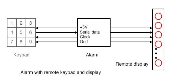
With the inclusion of the remote display, the figure "Alarm with remote key pad" from the parallel-in, serial-out section is replicated here.
As a result, we can see the status of the alarm loops connected to the main alarm box, for example.
If the Alarm finds an open window, it can notify us by sending serial data to the remote display.
Both the keypad and the display would likely be placed within the same remote enclosure, apart from the main alarm box. In this section, however, we will only look at the display panel.
We could just run eight wires to the eight LEDs, along with two wires for power and ground, if the display was on the same board as the Alarm.
On a long route to a remote panel, these eight wires are far less desired. Using shift registers, we just need to run five wires- clock, serial data, a strobe, power, and ground.
Even if the panel is only a few inches from the main board, reducing the number of wires in a connecting connection to improve dependability may be desired.
Also, we may use up all of a microprocessor's available pins and must resort to serial approaches to increase the number of outputs.
To receive data from microprocessors, several integrated circuit output devices, such as Digital to Analog converters, have serial-in, parallel-out shift registers.
The approaches shown here can be used on those sections as well.
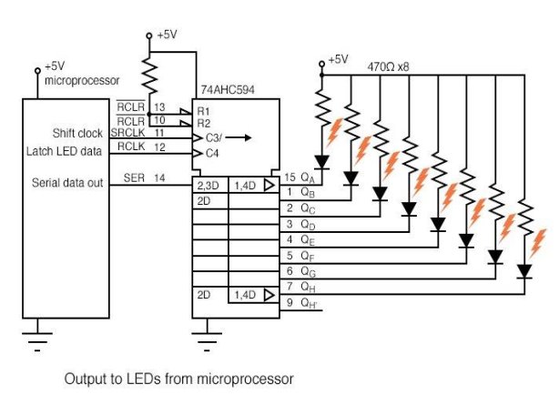
Although it requires an extra pin, RCLK, to parallel load the shifted-in data to the output pins, we chose the 74AHC594 serial-in, parallel-out shift register with output register.
This extra pin keeps the outputs from changing while the data is being transferred. LEDs don't have much of a problem with this. However, driving relays, valves, motors, and other similar devices would be problematic.
The microprocessor would begin by executing code that outputs 8 bits of data. On the "Serial data out" pin, one bit would be output, controlling the distant 74AHC594's SER.
The microprocessor then drives SRCLK of the ‘595 shift register with a low to high transition on “Shift clock.”
The data bit at SER is shifted from “D” to “Q” of the first shift register stage by this positive clock.
Because of the internal 8-bit output register between the shift register and the output pins, this has no effect on the QA LED at this moment (QA to QH).
Finally, the microprocessor reduces the value of “Shift clock.” The change of one bit into the ‘595 is now complete.
To complete the shifting of 8 bits of data from the microprocessor into the 74AHC594 serial-in, parallel-out shift register, repeat the previous technique seven more times.
The microprocessor must make a low to high transition on RCLK, the output register clock, to transfer the 8-bits of data from the internal ‘595 shift register to the output.
This updates the LEDs with updated information. In preparation for the next 8-bit data transfer, the RCLK must be brought back low.
Until the operation in the previous two paragraphs is repeated for a new 8-bits of data, the data at the output of the ‘595 will stay.
New data can be moved into the internal shift register of the ‘595 without altering the LEDs. Only when the RCLK rising edge is applied will the LEDs be updated with new data.
What if we require more than eight LEDs to be driven? Simply connect another 74AHC594 SER pin to the present shifter's QH'.
The SRCLK and RCLK pins should be parallel. Before creating an RCLK to feed both devices, the microprocessor would need to send 16 bits of data using 16 clocks.
We could be using 7-segment LEDs for the discrete LED indicators we've shown. There are, however, LSI (Large Scale Integration) devices that can drive multiple 7-segment digits.
This gadget accepts serial data from a CPU and uses multiplexing to drive more LED segments than it has pins.
4.8.3 The Shift Register
Another form of sequential logic circuit that can be used to store or transport binary data is the Shift Register.
The data on its inputs is loaded into this sequential device, which subsequently moves or "shifts" it to its output once every clock cycle, hence the name Shift Register.
A shift register is made up of many single-bit "D-Type Data Latches," one for each data bit, either a logic "0" or "1," coupled in a serial type daisy-chain arrangement, with the output of one latch becoming the input of the next, and so on.
Data bits can be fed in or out of a shift register serially, that is, one after the other from the left or right, or in a parallel configuration, all at the same time.
The number of individual data latches required to build up a single Shift Register device is normally dictated by the number of bits to be stored with the most common being 8-bits (one byte) wide formed from eight distinct data latches.
Shift Registers are used in calculators and computers for data storage or data transfer. They are typically used to store data such as two binary numbers before they are added together, or to transform data from serial to parallel or parallel to serial formats. A single shift register's individual data latches are all driven by the same clock ( Clk ) signal, making them synchronous devices.
Shift register ICs typically have a clear or reset connection, allowing them to be "SET" or "RESET" as needed. Shift registers generally function in one of four modes, with the basic data transfer through a shift register being:
Serial-in to Parallel-out (SIPO) - the register is filled one bit at a time with serial data, with the stored data available in parallel form at the output.
Serial-in to Serial-out (SISO) - under clock control, data is serially shifted "IN" and "OUT" of the register, one bit at a time in either a left or right direction
Parallel-in to Serial-out (PISO) - parallel data is concurrently loaded into the register and serially moved out of the register one bit at a time under clock control.
Parallel-in to Parallel-out (PIPO) - the parallel data is loaded into the register at the same time and transferred to their respective outputs at the same time using the same clock pulse.
The following graphic depicts the effect of data movement from left to right through a shift register:

A shift register's directional movement of data can be to the left (left shifting), to the right (right shifting), left-in but right-out (rotation), or both left and right shifting within the same register, resulting in bidirectional data movement. It is assumed in this course that all data shifts to the right (right shifting).
4.8.4 Basic Data Movement Through A Shift Register
Clock Pulse No | QA | QB | QC | QD |
0 | 0 | 0 | 0 | 0 |
1 | 1 | 0 | 0 | 0 |
2 | 0 | 1 | 0 | 0 |
3 | 0 | 0 | 1 | 0 |
4 | 0 | 0 | 0 | 1 |
5 | 0 | 0 | 0 | 0 |
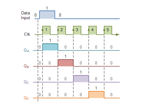
The 4-bits of data ( 0-0-0-1 ) are saved in the register after the fourth clock pulse has ceased and will remain there till the clocking of the register has finished. In actuality, the register's input data can be a variety of logic "1" and "0" combinations. The standard 8-bit 74LS164 or the 74LS594 are two SIPO ICs that are widely available.
Universal Shift Register
Many high-speed bi-directional “universal” type Shift Registers are now available, such as the TTL 74LS194, 74LS195, or the CMOS 4035, which are 4-bit multi-function devices that can be used in serial-to-serial, left shifting, right shifting, serial-to-parallel, parallel-to-parallel, or as a parallel-to-parallel multifunction data register, hence their name “Universal.”
These universal shift registers may execute any combination of parallel and serial input to output operations, but they require extra inputs to indicate the desired function as well as to pre-load and reset the device. The TTL 74LS194 is a widely used universal shift register, as shown below.
4-bit Universal Shift Register 74LS194
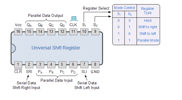
Universal shift registers are a type of digital gadget that can be used in a variety of situations. They can be designed to respond to actions that need temporary memory storage or information delay, such as the SISO or PIPO configuration modes, or to transfer data in a serial or parallel format from one place to another. In arithmetic operations, universal shift registers are widely used to shift data to the left or right for multiplication or division.
Shift Register Tutorial Summary
Then to summarise a little about Shift Registers
1. A simple Shift Register can be constructed with only D-type flip-Flops, one for each data bit.
2. Each flip-output flop's is connected to the D input of the flip-flop on the right.
3. Shift registers store data in memory that is relocated or "shifted" to its proper location on each clock pulse.
4. The contents of the register are shifted one bit to the left or right with each clock pulse.
5. In a series input (SI) arrangement, the data bits can be loaded one at a time or concurrently in a parallel arrangement (PI).
6. For a series output (SO), data can be removed one bit at a time; for a parallel output, data can be deleted all at once (PO).
7. Data conversion between serial and parallel, or parallel to serial, is one application of shift registers.
8. Shift registers are labelled as SIPO, SISO, PISO, PIPO, or a Universal Shift Register, which combines all functionalities into a single device.
In the next Sequential Logic Circuits tutorial, we'll look at what occurs when the output of the last flip-flop in a shift register is linked directly to the input of the first flip-flop, resulting in a closed loop circuit that constantly recirculates data. As a result, another sort of sequential logic circuit known as a Ring Counter is created, which is employed as a decade counter and divider.
4.9.1 Shift Registers: Parallel-in, Serial-out (PISO) Conversion
Parallel-in/ serial-out shift registers provide all of the functions of serial-in/ serial-out shift registers, plus they simultaneously input data to all stages.
The parallel-in/serial-out shift register saves data, shifts it clock by clock, and delays it by the number of stages multiplied by the clock period.
Furthermore, parallel-in/ serial-out means that we can load data into all stages in parallel before any shifting takes place.
This is a method for converting data from parallel to serial format. The data bits are present simultaneously on individual wires, one for each data bit, as seen below in a parallel manner.
The data bits are presented consecutively in time on a single wire or circuit in serial mode, as shown in the block diagram below for "data out."
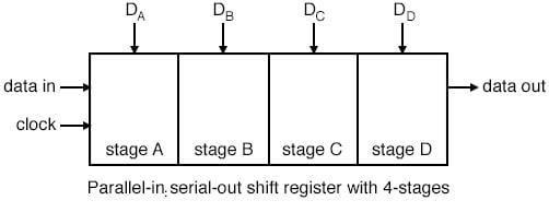
Parallel-in/ serial-out shift registers perform all of the tasks of serial-in/ serial-out shift registers, but they also input data to all stages at the same time.
Data is saved, shifted clock by clock, and delayed by the number of stages multiplied by the clock period in the parallel-in/serial-out shift register.
In addition, parallel-in/ serial-out means that data can be loaded into all stages in parallel before any shifting occurs.
This is a way for transforming parallel data to serial data. The data bits are present in a parallel way on individual wires, one for each data bit, as shown below.
In serial mode, the data bits are presented in temporal order on a single wire or circuit, as shown in the block diagram below for "data out."
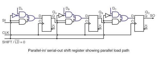
When SHIFT/LD' is logic low, the parallel load path is shown above. The top NAND gates that serve DA DB DC are enabled, and data is passed to the D inputs of type D Flip-Flops QA QB DC.
The data will be clocked from D to Q of the three FFs on the next positive going clock edge. At the same moment, three bits of data will be loaded into QA QB DC.
The form of parallel load as described, in which data loads on a clock pulse, is referred to as synchronous load since data loading is synced with the clock.
This must be distinguished from asynchronous loading, which is controlled by the preset and clear pins of the Flip-Flops and does not require the use of a clock.
Within a single device, only one of these load mechanisms is used, with synchronous load becoming more typical in newer devices.
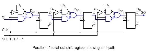
When SHIFT/LD' is logic high, the shift path is given above. The bottom AND gates of the pairs supplying the OR gate are activated, allowing us to connect SI to DA, QA to DB, QB to DC, and QC to SO in a shift register. Data will be right shifted out to SO on subsequent clock pulses as a result of clock pulses.
The waveforms below show both parallel loading and serial shifting of three bits of data. At DA DB DC, parallel data is transformed to serial data at SO.
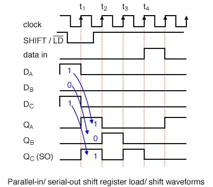
The waveforms above represent what we previously defined using words for parallel loading and shifting.
We'll use the parallel inputs DAA DBB DCC as an example. The SHIFT/LD' then goes low, allowing data to be loaded rather than shifted.
Due to setup and hold requirements, it must be low for a brief time before and after the clock pulse. It's a lot bigger than it needs to be.
It is, however, easier to make it wide with synchronous logic. We could have made the active low SHIFT/LD' almost two clocks wide, low almost a clock before t1, and high almost a clock before t3.
The crucial factor is that it must be low around clock time t1 in order for the clock to load the data in parallel.
Note that the data 101 at DA DB DC is timed from D to Q of the Flip-Flops at time t1, as indicated at QA QB QC
This is the synchronised parallel loading of data with the clock.
Now that the data has been imported, we can shift it if SHIFT/LD' is set to high, which it was before t2.
The data 0 at QC is shifted out of SO at t2, resulting in a waveform that is identical to the QC waveform. If nothing is attached to SO, it is either transferred into another integrated circuit or lost.
The data at QB is transferred to QC with a 0 value. The 1 at QA has been moved to QB. QA becomes 0 when “data in” is a 0. QA QB QC = 010 after t2.
QA QB QC = 001 after t3. This 1, which was previously only found in QA after t1, is now also found in SO and QC.
If an external integrated circuit exists, the last data bit is moved out to it. All data from the parallel load is lost after t4.
We see the shifting in of a data 1 present on the SI, serial input at clock t5.
Q: Why do shift registers have SI and SO pins?
A: These connections enable us to cascade shift register stages to create larger shifters than are possible in a single IC package. Serial connections to and from other ICs, such as microprocessors, are also possible.
Let's take a closer look at Texas Instruments' parallel-in/ serial-out shift registers, which are available as integrated circuits.
4.9.2 Parallel-in/serial-out devices
- Synchronous load SN74ALS166 parallel-in/ serial-out 8-bit shift register
- Asynchronous load SN74ALS165 parallel-in/ serial-out 8-bit shift register
- Synchronous load CD4014B parallel-in/ serial-out 8-bit shift register
- Synchronous load SN74LS647 parallel-in/ serial-out 16-bit shift register
The SN74ALS166 pictured above is the most accurate representation of the prior parallel-in/ serial-out shifter figures.
Let's have a look at the modest alterations to our diagram above. To begin with, there are eight stages. Only three are shown.
On the data sheet linked above, all eight steps are depicted. The data inputs A, B, C, and so on are labelled A, B, C, and so on by the manufacturer.
SH/LD' is the name of the SHIFT/LOAD control. It's shortened from our prior nomenclature, but the concept remains the same: parallel load if the load is low, shift if the load is excessive.
On the ALS166, the shift input (serial data in) is SER rather than SI. CLKINH, an inhibit signal, controls the clock CLK.
The clock is inhibited or deactivated if CLKINH is high. Otherwise, this "actual section" is identical to what we've already examined in depth.
On the data sheet, the ANSI (American National Standards Institute) symbol for the SN74ALS166 is shown above.
It's easier to hide the specifics within a symbol if we know how the part works. Symbols come in a variety of shapes and sizes.
The ANSI symbol has the advantage that the labels give suggestions about how the part works.
The control part of the ANSI symbol is the large notched block at the top of the ‘74ASL166. R has predicted that there will be a reset.
M1 (Shift), M2 (Load), and C3/1 (arrow) are the three control signals (inhibited clock). The clock serves two purposes.
The first is C3, which is used to shift parallel data wherever the prefix 3 appears. Second, anytime M1 is affirmed, as represented by the 1 of C3/1 (arrow), the data is moved to the right, as represented by the arrow.
These two functions are separated by a slash (/). The external inputs A, B, C, and H identify the 8-shift phases, as indicated by the title SRG8.
The internal 2, 3D implies that M2 [Load] and C3 clock control data, D. We can deduce that the parallel data is loaded synchronously with the clock C3 in this scenario.
To accommodate the input SER, the topmost level at A is a broader block than the rest.
M1 [Shift] and C3 clock control SER, according to the legend 1, 3D. As a result, when shifting rather than parallel loading, we expect to clock in data at SER.
The ANSI/IEEE basic gate rectangular symbols are shown above for comparison to the more common shape symbols so that we can figure out what the CLKINH and CLKpins on the previous ANSI SN74ALS166 symbol imply.
On the SN74ALS166 ANSI symbol, the CLK and CLKINH feed an OR gate. => on the rectangular inset symbol denotes OR.
A clock is indicated by the long triangle at the output. If there had been an arrow in the bubble, it would have signalled a shift on the negative clock edge (high to low).
The register shifts on the positive (low to high transition) clock edge since there is no bubble with the clock arrow.
The long arrow going right after the legend C3/1 implies a shift right, which is down the symbol.
The data sheet above reproduces part of the underlying logic of the SN74ALS165 parallel-in/ serial-out, asynchronous load shift register.
For the whole diagram, go to the link at the top of this page. Until now, we haven't looked at asynchronous data loading.
To begin, the loading is achieved by applying appropriate signals to the Flip-Flops' Set (preset) and Reset (clear) inputs.
The top NAND gates feed the FFs' Set pins and also cascade into the lower NAND gate, which feeds the FFs' Reset pins.
The signal travelling from the Set pin to the Reset pin is inverted by the bottom NAND gate.
To enable the upper and lower NAND gates, SH/LD' must first be brought low.
If SH/LD' was changed to a logic high instead of a logic low, the inverter feeding a logic low to all NAND gates would force a High out, releasing all FFs' "active low" Set and Reset pins.
The FFs could not be loaded because there would be no way to do so.
We can feed a data 1 to parallel input A, which inverts to a zero at the higher NAND gate output, setting FF QA to a 1 with SH/LD' kept low.
The 0 on the Set pin is sent to the bottom NAND gate, which inverts it to a 1, freeing the QA Reset pin.
As a result, data A=1 sets QA=1. The loading is asynchronous with respect to the clock because none of this requires it.
If we can't wait for a clock to parallel load data or generating a single clock pulse is difficult, we employ an asynchronous loading shift register.
The sole difference between feeding a data 0 to parallel input A and feeding a data 1 to parallel input A is that the data 0 inverts to a 1 out of the top gate, freeing Set.
This 1 at Set is inverted to a 0 at the lower gate, causing Reset to be pulled to a Low and QA=0 to be reset.
The internal controls C1 [LOAD] and C2 clock from the OR function of the SN74ALS166 are shown in the ANSI symbol above (CLKINH, CLK).
8-stage shifter, according to SRG8. Shifting right or down is indicated by the arrow after C2. As shown by internal label 2D, SER input is a clock function.
C1 [LOAD], represented by internal label 1D, is a function of the parallel data inputs A, B, C, and H.
Because of the half-arrow inverter at the input, C1 is asserted when sh/LD' =0.
Compare this to the prior synchronous ANSI SN75ALS166, which controlled the parallel data inputs via the clock. The ANSI Data labels differ from one another.
When LD/SH'=0 on the CD4014B, M1 is asserted. When LD/SH'=1, M2 is claimed.
When M2 is engaged, Clock C3/1 is utilised for parallel loading data at 2, 3D, as shown by the 2,3 prefix labels.
The internal 2,3 prefix labels for pins P3 through P7 are the same as for P2 and P8. The 1,3D prefix at SER denotes that M1 and clock C3 are required for serial data entry.
When M1 is active, as indicated by the 1 in the C3/1 arrow, right shifting occurs.
The CD4021B is similar to the CD4021A, with the exception that it supports asynchronous parallel data loading, as indicated by the lack of a 2 prefix in the data label 1D for pins P1, P2, and P8.
Prefix 2 in label 2D at input SER, of course, indicates that data is clocked into this pin. The clock is controlled by LD/SH', as seen by the OR gate inset.
The internal label SRG 16 on the SN74LS674 implies a 16-bit shift register.
1,2 M3 is the MODE input to the control area at the top of the symbol. As indicated by the 1,2 preceding M3, internal M3 is a function of input MODE and G1 and G2.
The AND function of any such G inputs is indicated by the base label G. G1/2 EN is the internal designation for input R/W.
This is an enable EN for tristate devices used elsewhere in the symbol (controlled by G1 AND G2).
It's worth noting that CS (pin 1) is internal G2. To get internal clock C4, chip select CS' is ANDed with input CLK.
The clock arrow's bubble indicates that activity is on the negative clock edge (high to low transition).
The slash (/) is a separator, signifying that the clock has two purposes. C4 indicates control of anything with a 4 prefix before the slash.
The 3' (arrow) after the slash denotes shifting. When M3 is de-asserted (MODE=0), the 3' of C4/3' denotes shifting. Shift right is indicated by the long arrow (down).
External inputs P0-P15, pins P0-P15, are located below the control section in the data section (7-11, 13-23).
M3 and the clock C4 govern loading of parallel data, as shown by the prefix 3,4 of internal label 3,4D.
Data is represented by the letter D. Although not expressly stated out, this label is presumed to apply to all parallel inputs.
On the right of the P0 (pin7) stage, look for the label 3',4D. The complemented-3 shows that M3=MODE=0 inputs (shifts) SER/Q15 (pin5) at clock time, using clock C4 (4 of 3',4D).
To put it another way, with MODE=0, we shift data from the serial input into Q0 (pin 6). At clock time, all other stages move right (down).
The triangle pointing right at the bottom of the symbol represents a buffer between Q and the output pin.
A tri-state gadget is indicated by the triangle pointing down. We previously indicated that enable EN, which is actually G1 AND G2 from the control section, controls the tristate.
The tri-state is disabled if R/W=0, and data can be shifted into Q0 via SER (pin 6), which we neglected earlier. MODE=0, R/W'=0, and CS'=0 are genuinely required.
The internal logic of the SN74LS674 is provided in the link in the bullet list at the beginning of the section, as well as a table describing the function of the control signals.
If R/W'=1, the tristate is enabled, and Q15 shifts out SER/Q15 (pin 6) and recirculates to the Q0 stage through 3',4D.
We assumed CS' was low, resulting in clock C4/3' and G2 being used to enable the tri-state.
4.9.3 Practical Applications
Reading data into a microprocessor is one application of a parallel-in/ serial-out shift register.
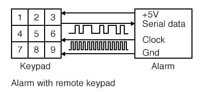
A remote keypad is used to operate the alarm system described above. To power the remote keypad, the alarm box provides +5V and ground.
The alarm sends shift clocks to the remote keypad, which returns serial data revealing the status of the keys via a parallel-in/ serial-out shift register every few tens of milliseconds.
As a result, we found nine key switches connected by four wires. If we had to run a circuit for each of the nine keys, how many wires would we need?
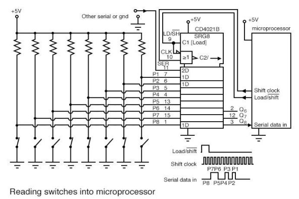
A parallel-in/ serial-out shift register can be used to read numerous switch closures into a microprocessor using only a few pins.
On an 8-pin package, some low-end microprocessors only have 6-I/O (Input/Output) pins.
Alternatively, we may have used the majority of the pins on an 84-pin package. The quantity of wires going around a circuit board, machine, vehicle, or structure may be reduced.
Our system's reliability will improve as a result of this. Manufacturers who minimise the amount of wires in an automobile generate a more reliable product, according to reports.
In any case, reading 8-bits of data from the switches in the diagram requires only three CPU pins.
Because it is easier to handle data loading without having to generate a single parallel load clock, we picked an asynchronous loading device, the CD4021B.
With a resistor on each input, the parallel data inputs of the shift register are brought up to +5V.
When the microprocessor shifts the LD/SH' line from low to high, then back low in preparation of shifting, all 1s will be loaded into the shift register if all switches are open.
Any switch closures will result in logic 0s being applied to the parallel inputs. The LD/SH'=1 created by the microprocessor software will parallel load the data pattern at P1-P7.
For each of the eight bits, the microprocessor generates shift pulses and reads a data bit.
This operation can be done entirely in software, or it can be done in hardware using one or more serial interfaces on bigger microprocessors.
The microprocessor makes a 0 to 1 transition on the Shift clock line when LD/SH'=0, and then reads a data bit from the Serial data in line. This is done for each of the eight bits.
If more switch contacts need to be read, another similar CD4021B circuit can be used to drive the SER line of the shift register.
The microprocessor will then generate 16-shift pulses. It'll most likely be driven by something else compatible with this serial data format, such as an analogue to digital converter, a temperature sensor, a keyboard scanner, or a serial read-only memory, for example.
Limit switches on a machine's carriage, an over-temperature sensor, a magnetic reed switch, a door or window switch, an air or water pressure switch, or a solid state optical interrupter are examples of switch closures.
4.9.4 Parallel in Serial Out (PISO) Shift Register
Data is loaded into Parallel In Serial Out (PISO) shift registers in parallel format and retrieved serially. In addition to the fundamental register components (flip-flops) fed with clock and clear pins, Figure depicts a PISO shift register with a control-line and combinational circuit (AND and OR gates).

The SH/LD control line is used to select the shift register's functionality between shift and load at any given time. This is because when the SH/LD line is set to low, all combinational circuits' A2 AND gates become active, while the A1 gates become dormant.
As a result, the bits of the input data word (Data in) that appear as inputs to the gates A2 are sent on as OR gate outputs at each combinational circuit. At the appearance of the first leading edge of the clock, the various bits of the Data in are loaded/stored into respective flip-flops (except the bit B1 which gets directly stored into FF1 at the first clock tick). This means that at the same clock tick, all the bits of the input data word are stored in the register components.
The SH/LD line is then driven high, activating the gates A1 of the combinational circuits and deactivating the gates A2. This enables the output bit of each flip-flop (save the last flip-flop FFn) to appear as the output of the OR gate driving the very-next flip-flop, i.e. the output bit of FF1 (Q1) appears as the output of OR gate 1 (O1) connected to D2; Q2 = output of O2 = D3, and so on. If the rising edge of the clock pulse appears at this point, Q1 appears at Q2, Q2 occurs at Q3, and so on. Qn-1 shows up at Qn.
This is nothing more than a one-bit right-shift of the data stored in the register. Similarly, one bit escapes the PISO shift register through the output pin of the nth flip-flop (Data out = Qn of FFn), which is nothing but the serial output, for each of the additional clock pulses applied. As a result, obtaining the whole n-bit input data word as a serial output of the PISO shift register needs n clock cycles.
Table depicts the PISO shift register's truth table, which emphasises the loading and retrieval processes, whereas Figure depicts the associated wave patterns.
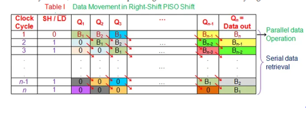
The data bits within the register can be shifted from right to left by minimally altering the design of Figure, resulting in a left-shift PISO shift-register. The core functioning idea, however, has not changed.
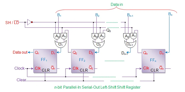
4.10.1 Shift Registers in Digital Logic
A single bit of binary data can be stored in a flip flop (1or 0). However, numerous flip flops are required to store several bits of data. To hold n bits of data, N flip flops must be connected in a specific order. A register is a device that is used to store this type of data. It consists of a series of flip flops used to hold numerous bits of data.
With the use of shift registers, the information held in these registers can be transferred. A shift register is a collection of flip flops that can hold multiple bits of information. By applying clock pulses to the bits contained in such registers, they can be made to move within the registers and in and out of the registers. By connecting n flip-flops, each of which holds a single bit of data, an n-bit shift register can be created.
"Shift left registers" are the registers that shift the bits to the left.
"Shift right registers" are the registers that shift the bits to the right.
Shift registers are basically of 4 types. These are:
1. Shift register with serial in and serial out.
2. Shift register with serial in parallel out.
3. Shift register (Parallel In Serial Out)
4. Shift register with parallel in parallel out.
Serial-In Serial-Out Shift Register (SISO) –
Serial-In Serial-Out shift register is a shift register that accepts serial input (one bit at a time through a single data line) and outputs serial data. The data leaves the shift register one bit at a time in a serial pattern because there is only one output, hence the term Serial-In Serial-Out Shift Register.
A serial-in serial-out shift register is shown in the logic circuit below. The circuit is made up of four D flip-flops connected in a serial fashion. Because each flip flop receives the same clock signal, they are all synchronised with one another.

The above circuit is an example of a shift right register, which accepts serial data from the flip flop's left side. A SISO's principal function is to act as a delay element.
Serial-In Parallel-Out shift Register (SIPO) –
Serial-In Parallel-Out shift registers allow serial input (one bit at a time through a single data line) and provide parallel output.
A serial-in-parallel-out shift register is shown in the logic circuit below. The circuit is made up of four D flip-flops that are connected together. To RESET the flip flops, the clear (CLR) signal is connected to them in addition to the clock signal. The first flip flop's output is connected to the next flip flop's input, and so on. Because each flip flop receives the same clock signal, they are all synchronised with one another.
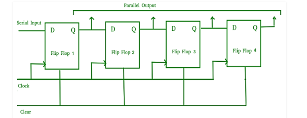
The above circuit is an example of a shift right register, which takes serial data from the flip flop's left side and produces a parallel output. Because the principal application of the SIPO register is to transform serial data into parallel data, they are utilised in communication lines when demultiplexing of a data line into several parallel lines is necessary.
Parallel-In Serial-Out Shift Register (PISO) –
Parallel-In Serial-Out shift registers allow parallel input (data is delivered independently to each flip flop and in a simultaneous manner) and provide a serial output.
A parallel-in-serial-out shift register is shown in the logic circuit below. The circuit is made up of four D flip-flops that are connected together. The clock input is connected to all of the flip flops directly, while the input data is connected to each flip flop individually via a multiplexer at the input of each flip flop. The preceding flip flop's output and parallel data input are connected to the MUX's input, while the MUX's output is connected to the next flip flop. Because each flip flop receives the same clock signal, they are all synchronised with one another.
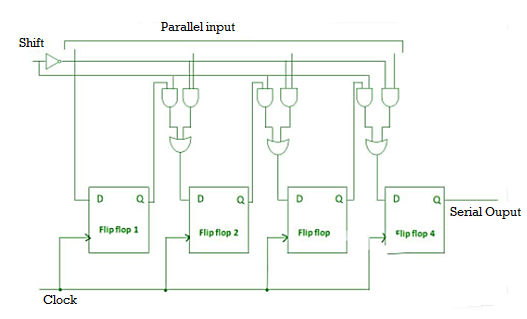
To convert parallel data to serial data, a Parallel in Serial Out (PISO) shift register is utilised.
Parallel-In Parallel-Out Shift Register (PIPO) –
Parallel-In parallel-Out shift register is a shift register that allows parallel input (data is delivered independently to each flip flop and in a simultaneous manner) and also provides a parallel output.
A parallel-in-parallel-out shift register is shown in the logic circuit below. The circuit is made up of four D flip-flops that are connected together. All four flip flops are connected to the clear (CLR) and clock signals. Because no serial shifting of data is necessary, there are no interconnections between the individual flip-flops in this sort of register. Data is delivered to each flip flop separately as input, and output is similarly gathered independently from each flip flop.
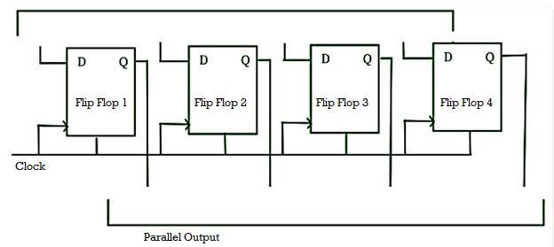
A PIPO shift register, like a SISO shift register, is utilised as a temporary storage device and also works as a delay element.
Bidirectional Shift Register –
Shifting a binary integer to the left by one place is equivalent to multiplying by 2; shifting a binary number to the right by one place is comparable to dividing by 2. We'll need a register that can shift data in either way to conduct these operations.
Bidirectional shift registers are registers that can shift data right or left depending on the mode. If you choose 1 (high), the data will be shifted to the right, and if you choose 0 (low), the data will be shifted to the left.
A bidirectional shift register is shown in the logic circuit below. The circuit is made up of four D flip-flops that are connected together. The input data is connected to two ends of the circuit, with only one active gate depending on the mode selected.
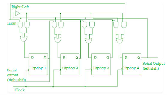
Shift Register Counter –
Shift Register Counters are shift registers that have their outputs wired back to their inputs to produce certain sequences. There are two types of these:
1. Ring Counter –
A ring counter is a shift register counter in which the output of the first flip flop is connected to the output of the second flip flop, and so on, with the output of the last flip flop being fed back to the input of the first flip flop. As long as clock pulses are applied, the data pattern within the shift register will circulate.
A Ring Counter is shown in the logic circuit below. The circuit is made up of four D flip-flops that are connected together. The data pattern will repeat every four clock pulses because the circuit consists of four flip flops, as illustrated in the truth table below:
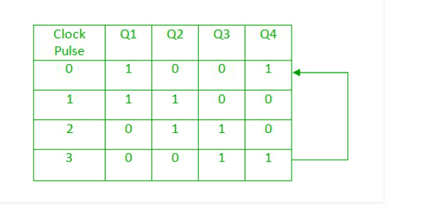
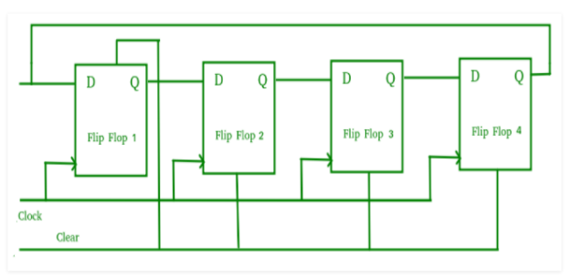
Ring counters are commonly utilised since they are self-decoding. To determine what state the counter is in, no further decoding circuit is required.
2. Johnson Counter
A Johnson counter is essentially a shift register counter in which the first flip flop's output is connected to the second flip flop's output, and so on, with the inverted output of the last flip flop being fed back to the first flip flop's input. Twisted ring counters are another name for them.
A Johnson Counter is shown in the logic circuit below. The circuit is made up of four D flip-flops that are connected together. A mod-2n counter is an n-stage Johnson counter that produces a count sequence of 2n different states. The data pattern will repeat every eight clock pulses because the circuit consists of four flip flops, as shown in the truth table below:
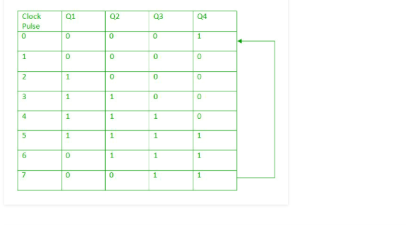

The fundamental advantage of the Johnson counter over the ring counter is that it only requires n flip-flops to circulate a given data and generate a sequence of 2n states.
Applications of shift Registers –
1. Shift registers are used to store temporary data.
2. Data transport and manipulation are also done with shift registers.
3. To add time delay to digital circuits, serial-in serial-out and parallel-in parallel-out shift registers are utilised.
4. The serial-in parallel-out shift register is employed in communication lines where demultiplexing of a data line into numerous parallel lines is necessary.
5. To convert parallel data to serial data, a Parallel in Serial out shift register is utilised.
4.10.2 Shift Registers – Types, Applications
Introduction
A single bit of binary data, such as 1 or 0, can be stored in a flip flop. However, numerous flip flops are required to store several bits of data. Because a single flip flop can only store one bit of information, n flip flops are connected in a specific way to store n bits of information. A register is a device in digital electronics that is used to store information.
In order to build registers, flip flops are used. A register is a collection of flip flops that can hold numerous bits of information. A set of 16 flip flops, for example, is required to store 16 bit data in a computer. A register's input and outputs might be serial or parallel, depending on the application.
Registers hold data bits in a series termed "Byte" or "Word," where a Byte is an 8-bit collection and a Word is a 16-bit collection (or 2 Bytes).
A Register is an arrangement in which a number of flip flops are connected in series. The stored data can be transferred between the registers, which are referred to as "Shift Registers." Every clock cycle, a shift register stores the data and shifts it towards the output.
Basically shift registers are of 4 types. They are
- Serial In Serial Out shift register
- Serial In parallel Out shift register
- Parallel In Serial Out shift register
- Parallel In parallel Out shift register
Serial in Serial Out Shift Register
The input to this register is serial, meaning it receives data one bit at a time through a single data line, and the output is also serial. The data can only be shifted to the left or right. As a result, it's known as a SISO shift register (Serial in Serial Out).
The shift register moves the data bits to the left as the data is fed from the right bit by bit. A four-bit SISO shift register has only three connections and four flip flops.
"Shift left registers" are the registers that shift the bits to the left.
"Shift right registers" are the registers that shift the bits to the right.
Example: If we pass the data 1101 to the data input, the shifted output will be 0110.

This is the simplest of the four types of registers. The serial data is attached to the left or right most flip flop because the clock signal is wired to all four flip flops. The first flip flop's output is connected to the next flip flop's input, and so on. The shift register's final output is collected at the farthest flip flop.
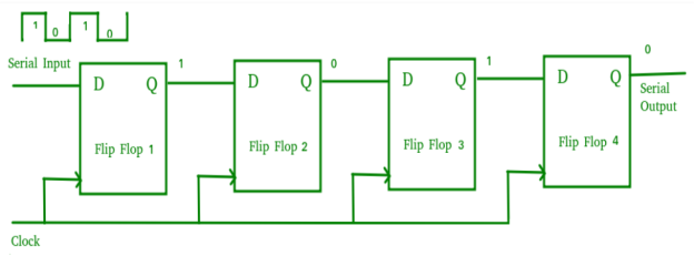
The shift right register is shown in the diagram above, feeding the serial data input from the left side of the flip flop arrangement.
When the clock signal is applied and the serial data is delivered to this shift register, only one bit at a time will be available at the output in the order of the input data. The SISO shift register is used as a data storage device that is only used temporarily. The major function of a SISO, however, is to operate as a delay element.
Serial in Parallel Out shift register
The input to this register is given in serial and the output is collected in parallel
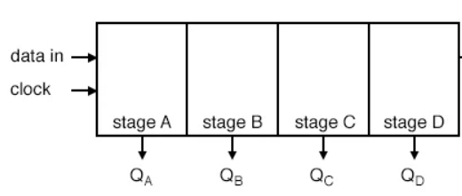
The clear (CLR) signal is connected to all four flip flops in addition to the clock signal to RESET them, and serial data is linked to the flip flop on either end (depending on shift left register or shift right register). The first flip flop's output is connected to the next flip flop's input, and so on. A common clock connects all of the flip flops.
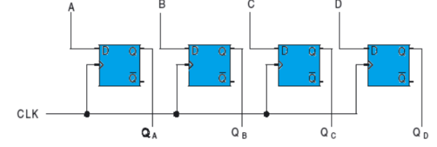
The output of the Serial in Parallel out (SIPO) shift register is gathered at each flip flop, unlike the serial in serial out shift registers. The outputs of the first, second, third, and fourth flip flips are Q1, Q2, Q3, and Q4, respectively.
Serial in Parallel out shift registers are used to convert serial data into parallel data. As a result, they're used in communication lines where demultiplexing a data line into multiple parallel lines is necessary.
Parallel in Serial out shift register
The data is fed into this register in parallel, that is, data is fed into each flip flop separately, and the output is gathered in serial at the final flip flop's output.

The clock input is connected directly to all of the flip flops, while the input data is connected to each flip flop individually via a mux (multiplexer) at the input. Individual parallel inputs to the shift register are D1, D2, D3, and D4. The output is serially gathered in this register.
.
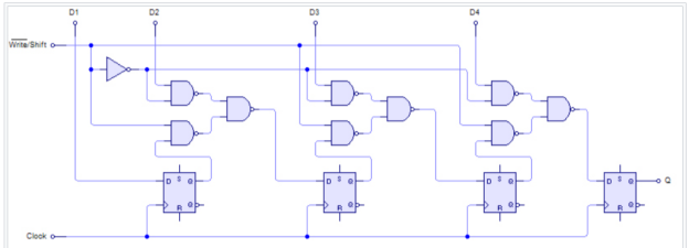
The preceding flip flop's output and parallel data input are connected to the MUX's input, while the MUX's output is connected to the next flip flop. Parallel data is converted to serial data using a Parallel in Serial Out (PISO) shift register. As a result, they're employed in communication lines that combine numerous data lines into a single serial data line.
Parallel in Parallel out shift register
The input is delivered in parallel, and the output is also gathered in parallel in this register. All four flip flops are connected to the clear (CLR) and clock signals. Data is delivered to each flip flop separately as input, and output is similarly gathered independently from each flip flop.
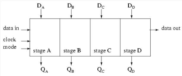
The four-stage parallel in parallel out register is depicted in the diagram above. The parallel outputs are Qa, Qb, Qc, and Qd, while the parallel inputs are Pa, Pb, Pc, and Pd. None of the four flip flops are connected to each other.
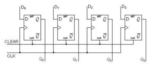
Similar to a SISO shift register, a Parallel in Parallel out (PIPO) shift register is utilised as a temporary storage device as well as a delay element.
4.10.3 Ring Counter
It is built as a feedback path by connecting the output of the first flip flop to the output of the next one, and the output of the last flip flop to the first one as input. As a result, this is referred to as a "Ring Counter."

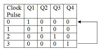
The first flip flop is connected to the high input, that is, its input is set to logic 1, and its output is connected to the input of the second flip flop, and so on.
Finally, the first flip flop receives the output of the last flip flop as input. When the first clock pulse is applied to the arrangement, the second stage input becomes 1 and the remainder inputs become 0. The input 1 is rotated around the ring in this manner.
Other Type of Registers
We also have other sorts of registers in addition to the ones listed above. Below is a list of them.
1. Shift register that can be used in both directions.
2. A shift register that is universal.
These registers are also employed in a variety of digital electronics applications.
Bidirectional Shift Register
Shifting a binary integer to the left by one position is the same as increasing the original value by two. Similarly, shifting a binary integer one position to the right is the same as dividing the original value by two.
As a result, a shift register with the ability to shift bits in either direction is required to conduct certain mathematical operations. Bidirectional Shift Register can help with this.
The above-mentioned shift registers are all Unidirectional Shift Registers, which means they only shift data to the right or left.
“The register in which the data can be shifted either left or right,” says the bidirectional shift register. This register has a right or left shift mode input, a clock signal, and two serial Data lines, one for input and the other for output.
The shift left and right actions will be controlled by the mode input. The data will be shifted right if the mode input is set to high (1). If the mode input is low (0), the data will be moved to the left. Below is a circuit for a bidirectional shift register utilising D flip flops.
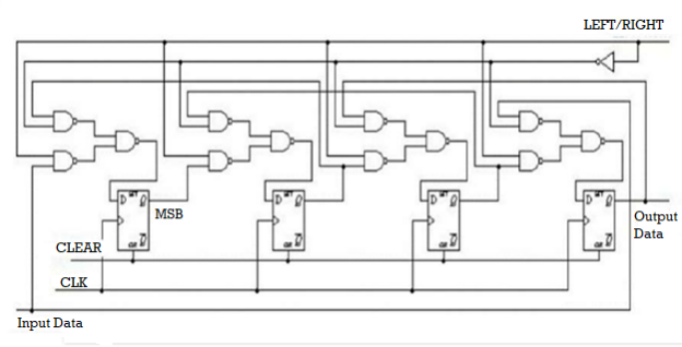
The circuit's input serial data is connected at both ends (to AND gates 1 and 8). Only one AND gate (either 1 or 8) is active depending on whether the mode input is high or low.
The serial data stream is AND1 – OR 1 – FF 1 – Q1 – AND 2 – OR 2 – FF 2 – Q2 – AND 3 – OR 3 – FF 3 – Q3 – AND 4 – OR 4 – FF 4 – Q4 when the mode input is high (Right / Left' = 1). (Serial Data OUT).
The serial data path is active when the mode input is low (Right / Left' = 0).
AND7 – OR 3 – FF 3 – Q3 – AND 6 – OR 2 – FF 2 – Q2 – AND 5 – OR 1 – FF 1 – Q1 – AND 8 – OR 4 – FF 4 – Q4 – AND 7 – OR 3 – FF 3 – Q3 – AND 6 – OR 2 – FF 2 – Q2 – AND 5 – OR 1 – FF 1 (Serial Data OUT).
Universal Shift Register
The universal shift register is defined as "a register that may be used to shift data in both directions, such as left and right, as well as load parallel data."
The three types of operations that this register can do are listed below.
1. Loading in parallel
2. Making a left turn
3. Shifting to the right.
This means the universal shift register can both store and send data in simultaneously. Similarly, by using shift left and shift right operations, data can be stored and transferred in a serial route.
Simply put, the universal shift register will input data in either serial or parallel and produce output in either serial or parallel, depending on our needs. It's known as the Universal Shift Register because it can perform left and right shifts, serial to serial, serial to parallel, parallel to serial, and parallel to parallel operations.
Construction
Take a look at the universal shift register logic gate representation below. The mode input is connected directly to the MUX input, while the reversed mode input (through the NOT gate) is routed to the upper stage flip flops' inputs.
The inputs D1, D2, D3, and D4 are connected in parallel, as are the outputs Q1, Q2, Q3, and Q4. For both left and right shift, it features a serial input pin that feeds data into the register. Below is a logic diagram for a four-bit universal shift register.

The circuit diagram of a 4 bit bidirectional universal shift register is shown.
Operation
1. To load the data in parallel, the mode input is set to high (MODE = 1). The mode input is wired to low (MODE = 0) for serial shifting.
2. The universal shift register will operate/behave as a bidirectional shift register when the mode pin is connected to GROUND.
3. To shift the data to the right, the serial input pin is linked to the AND gate – 1 of the first flip flop.
4. The input is connected to AND gate – 8 of the last flip flop; through input D, to shift the data to the left.
5. When S0 and S1 are both 0, the universal shift register is locked, which implies no operations are done.
6. When S0 = 1 and S1 = 0, the data is shifted to the right, resulting in a shift right operation.
7. When S0 = 0 and S1 = 1, the data is shifted to the right, resulting in a shift left operation.
When S0 and S1 are both zero, the register performs a PARALLEL LOAD operation.
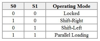
Because they have a 41 MUX at the input, the universal shift register will work in all of the modes listed above.
Applications of Shift Registers
Registers are employed in digital electrical devices such as computers for a variety of purposes.
1. Temporary data storage
2. Data transfer
3. Data manipulation
4. As counters.
Computers employ shift registers as memory elements. All digital systems must store huge amounts of data efficiently; to do so, we employ storage elements such as RAM and other types of registers.
Registers are used to perform several operations in digital systems, such as division and multiplication. Data is conveyed using serial shift registers and other similar devices.
Digital clocks, frequency counters, and binary counters are examples of counters.
For time delays, serial in – serial out registers are utilised.
The data is converted from serial to parallel form using serial in – parallel out registers. As a result, these are also known as "Serial to Parallel Converters."
The data is converted from parallel to serial form using parallel in – serial out registers. As a result, they're also known as "parallel to serial converters."
Delay Line
Greetings! The most common application of shift registers is the delay line. To add time delay to digital circuitry, a serial in serial out shift register is utilised. The following formula can be used to compute the time delay.
Δt = N * 1 / fc
N stands for the number of stages / flip flops, while fC stands for the clock frequency.
As a result, at output, an input pulse is delayed by t. The clock signal frequency or flip flops in the shift register regulate the amount of time delay.
4.11.1 Ring Counter
A counter is a computerised gadget that counts things. Flip-flops are bi-stable devices that are commonly used to create these. Generally, D or JK type flip-flops are used to construct counters, regardless of the type they are. This applies to ring counters as well. In reality, the type of connection that occurs between the flip-flops dictates the type of counter that is constructed.
Assume that we have connected all of the flip-flops in a series, with the output of the previous flip-flop feeding into the input of the next flip-flop. Let's also connect the last flip-output flop's to the first flip-flop in the chain as an input.
The resulting circuit is a ring counter with a length equal to the number of cascaded flip-flops. Figure depicts such an arrangement employing n D flip-flops, which is essentially an n-bit ring counter.
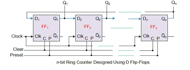
The preset (P) pin is used to load a specific bit pattern into the counter, while the clear (C) pin is used to clear all of the flip-flops in the chain. Ring counters are commonly loaded with a pattern in which all of the bits are zeros except for one, which is why they are also known as one-hot counters. A 4-bit ring counter, for example, will be loaded with the bit pattern 0001.
Because the last flip-output flop's is coupled to the first flip-flop, this bit pattern rotates within the counter by altering its position once for each clock pulse. This type of data movement causes the bit pattern to be repeated every n clock cycles, where n is the length of the counter.
Table shows one example of data transfer for a 4-bit ring counter pre-fed by the bit pattern 1000. The bit-pattern that was first given repeats every four clock pulses, as can be seen here. Figure illustrates the related waveforms.
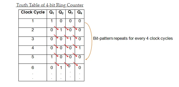
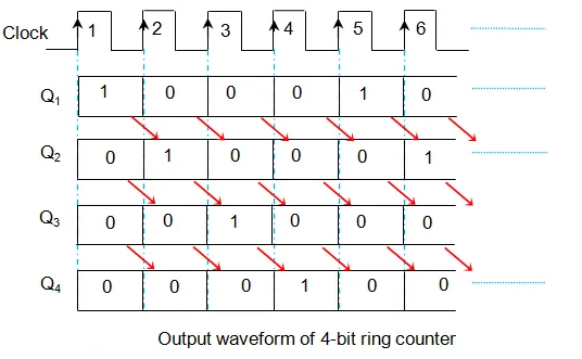
Merit
At any given time, ring counters have only one bit high. Unlike other counters that involve additional logic circuitry, they are easily decodable in nature.
Demerit
Instead of 2n valid states, an n-bit ring counter has only n valid states. They are inefficient in terms of state utilisation as a result of this.
4.11.2 Ring Counter in Digital Logic
Shift resisters are commonly used in ring counters. The ring counter is nearly identical to the shift counter. The main difference is that in a ring counter, the output of the last flip-flop is connected to the input of the first flip-flop, whereas in a shift resister, it is taken as output. Except for that, everything else is the same.
The number of states in the Ring counter equals the number of flip-flops utilised.
So we'll need four flip-flops to make a 4-bit Ring counter.
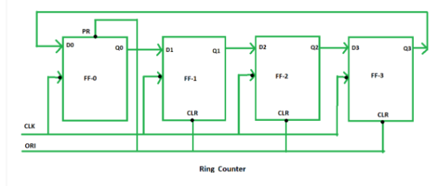
The clock pulse (CLK) is applied to all of the flip-flops at the same time in this diagram. As a result, it's a synchronised counter.
We also use Overriding input (ORI) for each flip-flop here. The ORIs are Preset (PR) and Clear (CLR).
When PR is 0 and the output is 1, the result is 1. When CLR is 0, the output is also 0. PR and CLR are both active low signals that always operate at a value of 0.
Q = 1 PR = 0 PR = 0 PR = 0 PR = 0
CLR = 0; Q = 0; CLR = 0; Q = 0; C
These two numbers are always the same. They are unaffected by the input D value or the Clock pulse (CLK).
Working –
In FF-0, ORI is tied to Preset (PR), whereas in FF-1, FF-2, and FF-3, it is tied to Clear (CLR). As a result, output Q = 1 is generated at FF-0, whereas output Q = 0 is generated by the rest of the flip-flop. Pre-set 1 is the output Q = 1 at FF-0 that is utilised to build the ring in the Ring Counter.
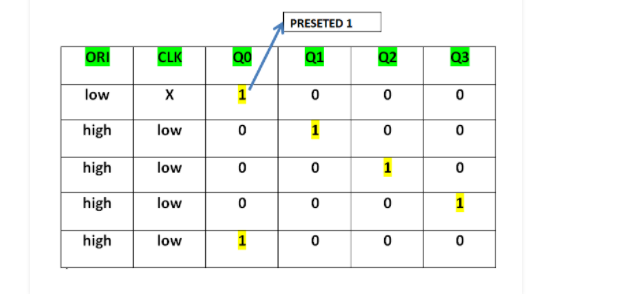
This Preseted 1 is created by setting ORI to zero and setting the time Clock (CLK) to don't care. After that, the ORI was set to high and a low clock pulse signal was applied as the clock (CLK) was triggered on the negative edge. The preset 1 is then transferred to the next flip-flop with each clock pulse, forming Ring.
We can deduce from the above table that the 4-bit Ring Counter has four states.
The following are the four states:
1 0 0 0
0 1 0 0
0 0 1 0
0 0 0 1
Using four D flip-flops, a 4-bit Ring Counter can be created.
Types of Ring Counter – There are two types of Ring Counter:
1. Straight Ring Counter –
One Hot Counter is another name for it. The output of the last flip-flop is connected to the input of the first flip-flop in this counter. The major feature of this Counter is that it circles the ring with a single one (or zero) bit.
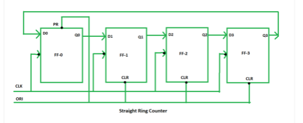
Here, we use Preset (PR) in the first flip-flop and Clock (CLK) for the last three flip-flop.
2. Twisted Ring Counter –
It's also known as a Johnson counter, a switch-tail ring counter, or a walking ring counter. It circulates a stream of ones followed by zeros around the ring by connecting the complement of the output of the final shift register to the input of the first register.
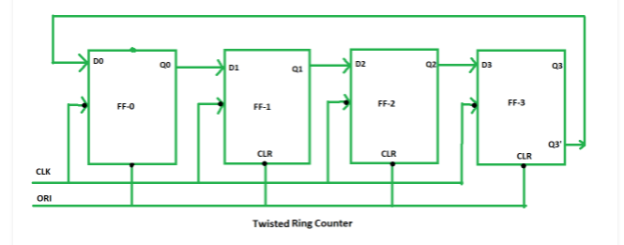
4.11.3 Digital Counters
A counter is a circuit that operates in a consecutive manner. The term "counter" refers to a digital circuit that counts pulses. The most common use of flip-flops is on the counter. A clock signal is applied to a collection of flip-flops. There are two sorts of counters.
- Asynchronous or ripple counters.
- Synchronous counters.
Asynchronous or ripple counters
Figure shows the logic diagram of a 2-bit ripple up counter. We're using a toggle (T) flip-flop. However, we can use the JK flip-flop with J and K permanently connected to logic 1. External clock is applied to flip-flop A's clock input, and the QA output is applied to the clock input of the following flip-flop, FF-B.
Logical Diagram

Operation
S.N. | Condition | Operation |
1 | Initially let both the FFs be in the reset state | QBQA = 00 initially |
2 | After 1st negative clock edge | FF-A will toggle and QA will equal 1 as soon as the first negative clock edge is applied. The clock input of the FF-B is connected to QA. FF-B treats QA as the positive clock edge because it has shifted from 0 to 1. Because FF-B is a negative edge triggered FF, there is no change in QB. After the first clock pulse, QBQA = 01
|
3 | After 2nd negative clock edge | When the second negative clock edge arrives, FF-A toggles again, and QA = 0. For FF-B, the change in QA operates as a negative clock edge. As a result, it will toggle, and QB will be 1. After the second clock pulse, QBQA = 10. |
4 | After 3rd negative clock edge | When the 3rd negative clock edge arrives, FF-A toggles again, and QA changes from 0 to 1. Because this is a favourable going change, FF-B ignores it and remains dormant. As a result, QB does not change and remains at 1. QBQA = 11 after the third clock pulse. |
5 | After 4th negative clock edge | When the 4th negative clock edge arrives, FF-A toggles again, and QA changes from 0 to 1. For FF-B, this negative change in QA functions as a clock pulse. As a result, it toggles QB from 1 to 0. After the fourth clock pulse, QBQA = 00. |
Truth Table
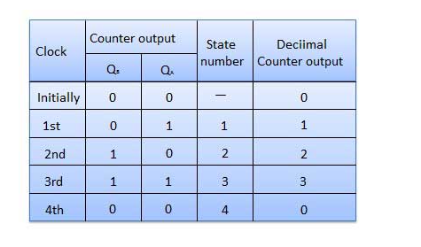
Synchronous counters
A synchronous counter is one in which the "clock" pulses are applied to all of the flip-flops in the counter at the same time.
2-bit Synchronous up counter
FF-JA A's and KA inputs are connected to logic 1. As a result, FF-A will function as a toggle flip-flop. QA is coupled to the JB and KB inputs.
Logical Diagram
Operation
S.N. | Condition | Operation |
1 | Initially let both the FFs be in the reset state | QBQA = 00 initially. |
2 | After 1st negative clock edge | FF-A will toggle and QA will change from 0 to 1 as soon as the first negative clock edge is applied. However, when a negative clock edge is applied, QA, JB = KB = 0. As a result, FF-B will remain in its current state. As a result, QB will remain at zero. After the first clock pulse, QBQA = 01 |
3 | After 2nd negative clock edge | FF-A toggles again when the second negative clock edge arrives, and QA switches from 1 to 0. However, QA was 1 at the time. As a result, JB = KB= 1 and FF-B toggle. As a result, QB goes from 0 to 1. After the second clock pulse, QBQA = 10. |
4 | After 3rd negative clock edge | When the third falling clock edge is applied, FF-A toggles from 0 to 1, but FF-B does not change state. After the third clock pulse, QBQA = 11. |
5 | After 4th negative clock edge | QA will change from 1 to 0 when the next clock pulse is applied, and QB will also shift from 1 to 0. After the fourth clock pulse, QBQA = 00. |
Classification of counters
The synchronous and asynchronous counters are classed as follows, depending on how the counting proceeds:
- Up counters
- Down counters
- Up/Down counters
- UP/DOWN Counter
An UP/DOWN counter is created by combining the up and down counters. A mode control (M) input allows you to choose between up and down mode. To achieve the up/down function, a combinational circuit must be built and employed between each pair of flip-flops.
Type of up/down counters
- UP/DOWN ripple counters
- UP/DOWN synchronous counter
- UP/DOWN Ripple Counters
All of the FFs in the UP/DOWN ripple counter operate in toggle mode. As a result, either T flip-flops or JK flip-flops must be worn. The clock is received directly by the LSB flip-flop. However, the clock for each subsequent FF is derived from the previous FF's (Q = Q bar) output.
● UP counting mode (M=0) – If up counting is to be achieved, the Q output of the preceding FF is connected to the clock of the next stage. The mode choose input M is set to logic 0 (M=0) for this mode.
● DOWN counting mode (M=1) − If M = 1, the previous FF's Q bar output is connected to the following FF. This will operate the counter in the counting mode.
Example
The ripple counter is a 3-bit binary up/down counter.
1. Three FFs are required because the data is 3-bit.
2. UP/DOWN As a result, a mode control input is required.
3. For a ripple up counter, the previous FF's Q output is connected to the following FF's clock input.
4. To make a ripple up counter, connect the Q output of the previous FF to the clock input of the next one.
5. For a ripple down counter, the previous FF's Q bar output is connected to the following FF's clock input.
6. Let the mode control input M govern the selection of Q and Q bar output of the preceding FF, so that if M = 0, UP counting occurs. As a result, connect Q to CLK. Counting down if M = 1. As a result, connect Q bar to CLK.
Block Diagram
Operation
S.N. | Condition | Operation |
1 | Case 1 − With M = 0 (Up counting mode) | When M = 0 and M bar = 1, the AND gates 1 and 3 in fig. Are activated, while the AND gates 2 and 4 are disabled. As a result, QA is connected to FF-clock B's input, while QB is attached to FF-clock C's input. These connections are the same as for a standard up counter. As a result, with M = 0, the circuit functions as an up counter. |
2 | Case 2: With M = 1 (Down counting mode) | When M = 1, AND gates 2 and 4 in the diagram are enabled, whereas AND gates 1 and 3 are disabled. As a result, QA bar is connected to FF-clock B's input while QB bar is connected to FF-clock C's input. A down counter will result from these connections. As a result, with M = 1, the circuit functions as a down counter. |
4.11.5 Modulus Counter (MOD-N Counter)
The MOD-4 counter is a 2-bit ripple counter, and the MOD-8 counter is a 3-bit ripple counter. An n-bit ripple counter is known as a modulo-N counter in general. Where 2n is the MOD number.
Type of modulus
- 2-bit up or down (MOD-4)
- 3-bit up or down (MOD-8)
- 4-bit up or down (MOD-16)
Application of counters
- Frequency counters
- Digital clock
- Time measurement
- A to D converter
- Frequency divider circuits
- Digital triangular wave generator.
Key takeaway:
A twisted ring counter, also known as a switch-tail ring counter, walking ring counter, Johnson counter, or Möbius counter, circulates a stream of ones followed by zeros around the ring by connecting the complement of the output of the final shift register to the input of the first register.
Create a four-bit ring counter using JK-FF and a timing diagram for it. The Q output of each stage of a flip flop is connected to the D output of the following stage in a Johnson Ring Counter. The last flip flop's complement output is connected to the rear of the first flip flop's input.
4.12.1 Asynchronous Counter
What is a Counter?
A counter is a gadget that can count the number of times a given event has occurred. This counter, which is based on a clock signal, may count and store the number of times any particular event or process has occurred in a digital logic system or computer. A sequential digital logic circuit with a single clock input and numerous outputs is the most common sort of counter. Binary or binary coded decimal numbers are represented by the outputs. Each clock pulse either increases or decreases the number of pulses.
What is Asynchronous?
The term asynchronous refers to the lack of synchronisation. Something that is neither present nor absent at the same moment. Asynchronous means regulating the operation time by sending a pulse only when the previous operation is done rather than transmitting it at regular intervals in a computer or telecommunication stream.
Asynchronous Counter
We now know what the term "counter" means and what the term "asynchronous" means. Asynchronous clock input can be used to count an asynchronous counter. Flip-flops can be used to make simple counters. Because the count is dependent on the clock signal, changing state bits are used as the clock signal for succeeding flip-flops in an asynchronous counter. The clock pulse ripples through the counter because the Flip-flops are serially coupled. It's often referred to as a ripple counter because of the ripple clock pulse. An asynchronous counter has a total of 2n - 1 counting states.
Asynchronous Truncated Counter and Decade Counter
Because Asynchronous counters, such as the MOD-16 with a resolution of 4-bit, have a maximum output number, it is also possible to utilise a basic Asynchronous counter in a setup where the counting state is less than the maximum output number. Modulo counters, often known as MOD counters, are one of those counters. The counter is setup in such a way that it resets to zero at a pre-determined value and has truncated sequences.
So, a complete sequence counter counts up to a certain number of resolutions (n-bit Resolution), and a truncated counter counts fewer than the maximum number.
The Asynchronous Truncated Counter can be used with combinational logic to take use of the asynchronous inputs in the flipflop.
The output of the Modulo 16 asynchronous counter can be adjusted with additional logic gates to provide a decade (divided by 10) counter output, which is useful in counting standard decimal values or in arithmetic circuits. Decade Counters are the name for this type of counter.
When the output reaches a decimal value of 10, Decade Counters must be reset to zero.
If we count 0-9 (10 steps) the binary number will be –
Number Count | Binary Number | Decimal Value |
0 | 0000 | 0 |
1 | 0001 | 1 |
2 | 0010 | 2 |
3 | 0011 | 3 |
4 | 0100 | 4 |
5 | 0101 | 5 |
6 | 0110 | 6 |
7 | 0111 | 7 |
8 | 1000 | 8 |
9 | 1001 | 9 |
As a result, the counter must be reset when the output hits 1001 (BCD = 9). We must pass this condition back to the reset input to reset the counter. A BCD or Binary-coded Decimal counter is one that counts from 0000 (BCD = 0) to 1001 (BCD = 9).
4.12.2 Timing Diagram of Asynchronous Decade Counter and its Truth Table
In the diagram above, a basic Asynchronous counter with four JK Flip-Flops and one 74LS10D NAND gate is utilised as a decade counter. On each clock pulse, the Asynchronous counter counts up from 0000 (BCD = 0) to 1001 (BCD = 9). Each JK flip-flop output generates a binary digit, which is then sent into the next flip-flop as a clock input. The output D, which is the Most Significant bit, and the output A, which is the Least Significant bit, are both in Logic 1 in the final output 1001, which is 9 in decimal. These two outputs are connected across the input of the 74LS10D. The output of the 74LS10D switches from Logic High or 1 to Logic Low or 0 when the next clock pulse is received.
When the 74LS10D changes its output, the 74LS73 J-K Flip-flops are reset since the NAND gate's output is wired to the 74LS73 CLEAR input. When the flip-flops were reset, the outputs from D to A were all reset to 0000, and the NAND gate output was reset to Logic 1. The upper circuit in the illustration becomes Modulo-10, or a decade counter, with this setup.
The Truth table of Decade counter is shown in the next table-
Clock Pulse | Decimal Value | Output - D | Output – C | Output – B | Output - A |
1 | 0 | 0 | 0 | 0 | 0 |
2 | 1 | 0 | 0 | 0 | 1 |
3 | 2 | 0 | 0 | 1 | 0 |
4 | 3 | 0 | 0 | 1 | 1 |
5 | 4 | 0 | 1 | 0 | 0 |
6 | 5 | 0 | 1 | 0 | 1 |
7 | 6 | 0 | 1 | 1 | 0 |
8 | 7 | 0 | 1 | 1 | 1 |
9 | 8 | 1 | 0 | 0 | 0 |
10 | 9 | 1 | 0 | 0 | 1 |
11 | 0 | 0 | 0 | 0 | 0 |
The below image is showing the timing diagram and the 4 outputs status on the clock signal. The reset pulse is also shown in the diagram.
Creating the Asynchronous Counter, Example, and Usability
Using the same way as for truncating counter output, we can change the Asynchronous counter's counting cycle. We can alter the input connection across the NAND gate or add additional logic gates configurations for alternative counting cycles.
The largest modulus that can be accomplished with n numbers of flip-flops is 2n, as we previously discussed. If we wish to make a truncated asynchronous counter, we should discover the lowest power of two that is either higher or equal to the modulus we require.
For example, if we wish to count from 0 to 56 or mod – 57 and then repeat from 0, the highest number of flip-flops necessary is n = 6, which results in a modulus of 64. The modulus will not be sufficient to count the numbers from 0 to 56 if we choose fewer flip-flops. If we use n = 5, the maximum MOD will be 32, which is not enough for the count.
To get MOD-128 or more specified counter, we can cascade two or more 4-bit ripple counters and configure each one as “divided by 16” or “divided by 8” arrangements.
In the 74LS section, the 7493 IC might be designed in such a way that we achieve a “divide by 128” frequency divider by configuring one 7493 chipset as a “divided by 16” counter and cascading another 7493 chipset as a “divided by 8” counter.
Other ICs, such as the 74LS90, have a programmable ripple counter or divider that may be adjusted to divide by 2, 3, 5, or other combinations.
The 74LS390, on the other hand, is a versatile option that may be utilised for massive division by a number ranging from 2 to 50,100 and other combinations.
4.12.3 Frequency Dividers
One of the most effective use of the asynchronous counter is as a frequency divider. We can reduce the frequency of a high-frequency clock to a useful, stable value that is significantly lower than the actual high-frequency clock. In the case of digital electronics, timing-related applications, digital clocks, and interrupt source generators, this is quite beneficial.
Assume we're using a traditional NE555 timer IC, which is a Monostable/Astable Multivibrator that runs at 260 kHz and has a +/- 2% stability. We can easily add an 18-bit ripple counter that is “Divided by 2” to create a 1 Hz reliable output that can be used to generate 1-second of delay or 1-second of pulse for digital clocks.

This is a simple circuit that divides the frequency using a ripple counter to produce stable frequency or timing from an unstable source. Other than signal generators, more exact crystal oscillators may provide precise high frequency.
Advantages and Disadvantages of Asynchronous Counter
Type D flip-flops make it simple to create asynchronous counters. They can be built using a “divide by n” counter circuit, which provides a lot more flexibility for applications that require a huge counting range, and the truncated counter can generate any modulus number count.
Despite these advantages, Asynchronous counter has significant drawbacks and restrictions.
When using the Asynchronous counter, resynchronizing the flipflops necessitates the use of additional re-synchronizing output flip-flops. Additionally, when the truncated sequence count is not equal to, further feedback logic is required.
When counting a large number of bits, the chain system caused the propagation delay between consecutive stages to become excessively significant, making it difficult to eliminate. Synchronous counters are faster and more trustworthy in this case. When high clock frequencies are applied across the Asynchronous Counter, there are additional counting mistakes.
4.12.4 Asynchronous Decade Counter
Starting at 0000 and counting higher on each trailing edge of the input clock signal until it reaches output 1001, this form of asynchronous counter is used (decimal 9). Both QA and QD outputs are now equal to logic "1." The output of the 74LS10 NAND gate changes state from logic "1" to logic "0" when the next clock pulse is applied.
Because the NAND gate's output is connected to all of the 74LS73 J-K Flip-flops' CLEAR ( CLR ) inputs, this signal causes all of the Q outputs to be reset to binary 0000 on the count of ten. Because the flip-flops have just been reset, outputs QA and QD are now both equal to logic "0," the NAND gate's output returns to a logic level "1," and the counter resets to 0000. We now have a decade counter, or Modulo-10.
Decade Counter Truth Table
Clock Count | Output bit Pattern | Decimal Value | |||
QD | QC | QB | QA | ||
1 | 0 | 0 | 0 | 0 | 0 |
2 | 0 | 0 | 0 | 1 | 1 |
3 | 0 | 0 | 1 | 0 | 2 |
4 | 0 | 0 | 1 | 1 | 3 |
5 | 0 | 1 | 0 | 0 | 4 |
6 | 0 | 1 | 0 | 1 | 5 |
7 | 0 | 1 | 1 | 0 | 6 |
8 | 0 | 1 | 1 | 1 | 7 |
9 | 1 | 0 | 0 | 0 | 8 |
10 | 1 | 0 | 0 | 1 | 9 |
11 | Counter Resets its Outputs back to Zero | ||||
Decade Counter Timing Diagram
The above circuit might easily be extended to different counting cycles by simply modifying the connections to the NAND gate inputs or by utilising other logic gate combinations based on the similar principle of truncating counter output sequences.
So, for example, a scale-of-twelve (modulo-12) can be readily created by simply taking the inputs to the NAND gate from the outputs at "QC" and "QD," keeping in mind that the binary equivalent of 12 is 1100 and that output "QA" is the least significant bit (LSB).
Because the highest modulus that can be implemented with n flip-flops is 2n, you should choose the lowest power of two that is larger than or equal to your desired modulus when building truncated asynchronous counters.
Let's pretend we want to count from 0 to 39, or mod-40, and then do it again. Then the greatest number of flip-flops necessary would be six, n = 6, resulting in a maximum MOD of 64, as five flip-flops would be insufficient, yielding a MOD-32.
If we were to make a “divide-by-128” counter for frequency division, we'd have to cascade seven flip-flops because 128 = 27. We would still need four ICs to complete the circuit if we used dual flip-flops like the 74LS74.
One simple approach is to utilise two TTL 7493s as 4-bit ripple counters and divisions. One 7493 might be setup as a "divide-by-16" counter and the other as a "divide-by-8" counter because 128 = 16 x 8. As indicated, the two ICs are cascaded together to make a "divide-by-128" frequency divider.
Standard IC asynchronous counters, such as the TTL 74LS90 programmable ripple counter/divider, can be programmed as a divide-by-2, divide-by-5, or any combination of the two. The 74LS390 is a versatile dual decade driver IC with a wide range of "divide-by" options, including divide-by-2, 4, 5, 10, 20, 25, 50, and 100.
Frequency Dividers
Because of the ripple counter's capacity to truncate sequences into a "divide-by-n" output, counters, particularly ripple counters, can be used as frequency dividers to lower a high clock frequency to a more acceptable value for use in digital clocks and timing applications. Consider the case when we need a precise 1Hz timing signal to run a digital clock.
A common 555 timer chip set as an Astable Multivibrator might easily output a 1Hz square wave signal, but the manufacturers data sheet states that the 555 timer has a normal 1-2 percent timing error depending on the manufacturer, which is not good at low frequencies like 1Hz.
However, the data sheet also states that the 555 timer's maximum operating frequency is around 300kHz, and that a 2% mistake at this high frequency, though still significant at roughly 6kHz maximum, is tolerable. We may easily produce a precision 1Hz timing signal by using a higher timing frequency, such as 262.144kHz, and an 18-bit ripple (Modulo-18) counter, as illustrated below.
4.12.5 1Hz timing signal from a 18-bit asynchronous ripple counter

Of course, this is a very simplified example of how to produce accurate timing frequencies, but precision frequency generators can be produced for a wide range of applications, from clocks and watches to event timing and even electronic piano/synthesizer or music type applications, using high frequency crystal oscillators and multi-bit frequency dividers.
Unfortunately, due to the internal circuitry of the gate, one of the main disadvantages of asynchronous counters is that there is a slight delay between the arrival of the clock pulse at its input and its presence at its output.
This delay is known as the Propagation Delay in asynchronous circuits, earning the asynchronous ripple counter the nickname "propagation counter," and in some high-frequency applications, this delay can cause misleading output counts.
In big bit ripple counter circuits, the difference in time between the input signal and the counted output signal can be quite significant if the delays of the individual stages are added up to create a cumulative delay at the end of the counter chain. As a result, the Asynchronous Counter is rarely employed in high-frequency counting circuits involving huge amounts of bits.
Due to its clocking sequence, the counter's outputs do not have a set time relationship with one another and do not occur at the same moment. To put it another way, the output frequencies become available one by one, creating a domino effect. The maximum working frequency of an asynchronous counter chain decreases as more flip-flops are added, ensuring accurate counting. Synchronous Counters were created to solve the problem of propagation delay.
Then, to summarise some of the benefits of asynchronous counters, consider the following:
1. Non-synchronized Toggle or D-type flip-flops can be used to make counters.
2. They're dubbed "Asynchronous Counters" since the flip-flops' clock inputs aren't all driven by the same clock signal.
3. A change in state from the preceding flip-flops output is required for each output in the chain.
4. Asynchronous counters are sometimes known as ripple counters because the data seems to "ripple" from one flip-output flop's to the next's input.
5. “Divide-by-n” counter circuits can be used to implement them.
6. Any modulus number count can be produced using truncated counters.
7. Asynchronous Counters' Drawbacks:
8. It's possible that an extra "re-synchronizing" output flip-flop is required.
9. Extra feedback circuitry is necessary to count a truncated sequence that is not equal to 2n.
10. When a high number of bits are counted, the propagation delay between stages may become unacceptably long.
11. They're known as "Propagation Counters" because of this delay.
12. At high clocking frequencies, counting errors occur.
13. Because all flip-flops use the same clock signal, synchronous counters are faster and more reliable.
In the following tutorial about >Counters, we'll look at the Synchronous Counter, and see how the clock input of each flip-flop in the chain is connected to all of the flip-flops in the chain, allowing them to be clocked at the same time.
4.12.6 Different types of Asynchronous counters
There are many types of Asynchronous counters available in digital electronics. They are
- 4 bit synchronous UP counter
- 4 bit synchronous DOWN counter
- 4 bit synchronous UP / DOWN counter
4. Asynchronous 4-bit UP counter
In the diagram above, a 4 bit asynchronous UP counter with D flip flop is depicted. It has the ability to count numerals from 0 to 15. The clock inputs of all flip flops are cascaded, and each flip flop's D input (DATA input) is connected to one of the flip flop's state outputs.
Each active edge or positive edge of the clock signal will toggle the flip flops. The first flip flop is connected to the clock input. The clock signal is input to the other flip flops in the counter via Q' output of the previous flip flop. When the clock signal has a positive edge, the output of the first flip flop will change.
The flip flops in the asynchronous 4-bit up counter are connected in toggle mode, thus if the clock input is connected to the first flip flop FF0, the output after one clock pulse is 20.
The clock input of the next flip flop is triggered by the rising edge of the Q output of each flip flop. It sets the next clock frequency to half of the input frequency. The count of the 4 bit UP counter is represented by the Q outputs of each individual flip flop (Q0, Q1, Q2, Q3) (8).
The operation of an asynchronous up counter is described below.
Assume that the flip flops' four Q outputs are originally set to 0000. When the rising edge of the clock pulse is applied to the FF0, the output Q0 changes to logic 1 and the output Q0 changes to logic 0 with the following clock pulse. This signifies that the clock pulse's output state toggles (from 0 to 1) for one cycle.
Because the clock input of FF1 is connected to the Q' of FF0, the clock input of the second flip flop becomes 1. As a result, the output of FF1 is high (i.e. Q1 = 1), indicating a value of 20. As a result, the following clock pulse will cause Q0 to become high once more.
As a result, both Q0 and Q1 are now high, making the four-bit output 11002. When we apply the fourth clock pulse, it toggles the FF2 and sets the Q0 and Q1 to low states. As a result, the output Q2 will be 00102. Because this is a four-bit up counter, the output is a binary sequence ranging from 0 to 15, or 00002 to 11112. (0 to 1510).
For example, if the present count = 3, then the up counter will calculate the next count as 4.
Asynchronous 4-bit DOWN counter
In the diagram above, a 4 bit asynchronous DOWN counter is displayed. The UP counter can be easily modified. The DOWN counter is a four-bit counter that counts numbers from 15 to 0 downwards. All flip flops' clock inputs are cascaded, and each flip flop's D input (DATA input) is connected to logic 1.
At each active edge (positive edge) of the clock signal, the flip flops will toggle. The first flip flop is connected to the clock input. The clock signal is input to the other flip flops in the counter from Q output of the previous flip flop, rather than Q' output.
The four-bit down counter's count is represented by Q0, Q1, Q2, and Q3. When the positive edge of the clock signal occurs, the output of the first flip flop changes. If the current count is 3, for example, the up counter will calculate the following count as 2. The input clock will cause the next flip-output flop's (count) to shift.
The operation of the down counter is the polar opposite of that of the up counter. Every clock pulse at the input reduces the number of flip flops in the circuit. As a result, the down counter counts from 15, 14, 13,...0, or 11112 to 00002.
Although asynchronous, clock-based counters are used in both up and down counters, they are not extensively used due to their unreliability at high clock speeds.
4.12.7 What is clock ripple?
Clock ripple is the sum of the time delays of individual clock pulses that drive the circuit. In each flip flop, the logic gates will cause propagation delay, as shown in the diagram below.
Blue lines reflect the propagation delays of logic gates. Each of them will add to the delay of the next flip flop, and the total delay of the circuit is known as the propagation delay.
Each time the outputs of all flip-flops change at distinct time intervals and for different clock signal inputs, a new value appears at the output. For example, at clock pulse 8, the output should shift from 11102 (710) to 00012 (810) after a 400-700 nanosecond delay (Nano Seconds).
The sequence will change for clock pulses other than 8.
Although this drawback prevents the circuit from being used as a reliable counter, it is still useful as a simple and effective frequency divider, as each flip-flop in the chain divides the frequency by two. It's all about clock ripple in this case.
4.12.8 Asynchronous 3-bit up/down counters
We may create an asynchronous up/down counter by combining the concepts of UP and DOWN counters. Below is a three-bit asynchronous up/down counter.
It can count in either ways, up to down or down to up, based on the clock signal input.
UP Counting
If the UP and down inputs are 1 and 0, the non inverted output of FF 0 will be passed to the clock input of FF 1 via the NAND gates between the first and third flip flops. Similarly, the clock input of FF 2 will receive the Q output of FF 1. As a result, the UP/down counter does up counting.
DOWN Counting
If the DOWN and UP inputs are 1 and 0, the inverted output of FF 0 will be passed to the clock input of FF 1 through the NAND gates between the first and third flip flops. Similarly, the clock input of FF 2 will receive the Q output of FF 1. As a result, the UP/down counter counts down.
Because the addition propagation delay is added to the NAND gate network, the up/down counter is slower than an up counter or a down counter.
4.13.1 Decade Counter (BCD Counter)
BCD or Decade Counter Circuit
A binary coded decimal (BCD) counter is a ten-digit serial digital counter. It also resets with each new clock input. It's also known as a "Decade counter" because it can cycle through 10 different output combinations. 0000, 0001, 0010, 1000, 1001, 1010, 1011, 1110, 1111, 0000, 0001, and so on can be counted by a BCD counter.
A four-bit binary counter can be used as a decade counter by skipping any six of the sixteen (24) outputs. ICs for decade counters, such as the 74LS90, are commonly accessible and can be used in our circuit. It's a decade counter that runs asynchronously.
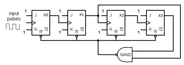
A decade counter built from JK flip flops is shown on the diagram above. Logic 1 is connected to both the J and K outputs. Except for the last one, every flip flop's clock input is connected to the output of the following flip flop.
All of the flip flops have their output wired in parallel to the clear input ‘CLR' of the NAND gate. This ripple counter may count up to 16 times, or 24 times in total.
Decade Counter Operation
The count is equal to 0000 while the Decade counter is at REST. The counter cycle begins with this stage. When a clock signal is connected to the counter circuit, the circuit counts the binary sequence. The first clock pulse can count up to nine times in the circuit (1001). The following clock pulse counts up to ten (1010).
Then the X1 and X3 ports will be high. The NAND gate output will be low for high inputs, as we know. Because the NAND gate output is connected to the clear input, the decade counter's flip flop stages are all reset. This means that after count 9, the pulse will begin counting from zero again.
Truth Table of Decade Counter
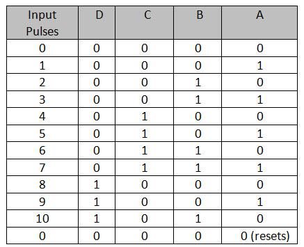
The Decade counter's counting operation is described in the table above. It is the circuit count for the decimal count of input pulses. When the count hits ten, the NAND gate output is zero (1010).
The inputs of NAND gates X1 and X3 decode the count. The logic gate NAND will trigger its output from 1 to 0 after count 10, and all flip flops will be reset.
State Diagram of Decade Counter
The Decade counter's state diagram is shown below. If we look at the decade counter circuit diagram, we can see that it has four stages, each with a single flip flop. As a result, it can count up to 16 bits or 16 possible states, however only 10 are used. The count goes from 0000 (zero) to 1001 (nine), after which the circuit is reset by the NAND gate.
To count up to any desired number, multiple counters are connected in series. The “Mod” or “Modulus” of a counter circuit refers to the number that it can count. The term "Mod- n counter" or "Modulo- n counter" refers to a counter that resets itself after counting n bits.
From 0 to 2n-1, the Mod n counter can calculate. Counters of many varieties are available, including Mod 4 counters, Mod 8 counters, Mod 16 counters, and Mod 5 counters, among others.
4.13.2 Commonly available Decade counter IC’s
The most commonly utilised ICs for designing a decade counter are the 4017B and 7049. The purpose of the other generally available integrated circuits (ICs) for Decade counter is described below.
4.13.3 74LS90 decade counter IC description
The IC 74LS90 is one most used chip we use to design decade counter.
Pin configuration
Explanation
It's a basic counter that counts from 0 to 9. It has four output ports: QA, QB, QC, and QD, as it is a four-bit binary decade counter. Every time the count hits ten, the binary output is reset to 0 (0000), and a new pulse is initiated at pin number nine. Change the RESET pins R1, R2, R3, R4 to change the Mod of the IC 7490.
If any of R1 and R2 are set to high or R3 and R4 are set to ground, the counter will reset all of the QA, QB, QC, and QD outputs to 0. The count on QA, QB, QC, and QD is 1001 if the pins R3 and R4 are high.
We may expand the counting capability of a Decade number by connecting more ICs in series, as we saw earlier; for example, two 7490 ICs connected in series can count 99. Divide by 2 and Divide by 5 counters are incorporated into the 7490 IC.
It can also be used as a divide-by-ten counter by connecting clock input 2 and QA, grounding all rest pins, and setting the pulse input to 1. By delivering a pulse at input 1, grounding reset pins R3 and R4, and connecting QA to input 2, it may be utilised as a divide by 6 counter.
The 7490 IC can be used as a bi-quinary counter, which stores decimal digits as 4 bit binary numbers.
Description of the 4017 CMOS decade counter IC

Applications of BCD Counter or Decade Counters
The key advantages and benefits if BCD counters are
5 Clock generation
6 Clock division
7 Integrated oscillator
8 Low power cmos
9 TTL compatible inputs
10 In frequency counting circuits
4.13.4 Decade counter in Frequency Counting
Binary counters can be used to design frequency counters. The circuit design for frequency counter is given below by using decade counter (designed by JK flip flops).
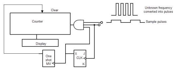
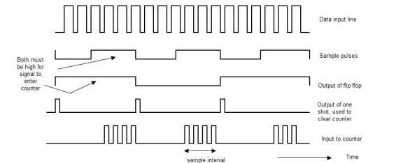
E provided the unknown frequency to one input and sample pulses to another input of the AND gate to count the frequency of the unknown counter. The input signal is allowed to flow to the counter when the sample pulses are at a high level; otherwise, low level sample pulse input is not allowed.
The number of counts divided by the sample time interval gives the frequency of the unknown signal. A JK flip flop provides the AND gate's third input, which is used to store the counter's produced output or result.
When both the JK flip flop input and the sample pulse input are high, the output reaches the counter. A one-shot multivibrator will reset the counter for each positive going edge of the JK flip flop by sending a pulse to it.
4.13.5 Decade Counter | Counter Circuit Basics
In today's electronics, a decade counter is fairly prevalent. The IC CD7490, which is most typically found in bigger integrated circuits, comprises numerous flip flops to convert BCD to decimal.
A decade counter counts from one to ten and then resets to zero after the ninth count.
Decade Counter Circuit Diagram

In general, counters can be easily built using register-type circuits. Aside from the decade counter, there are a number of other tools that are frequently used. Let's take a closer look.
Asynchronous counter
An asynchronous counter is a D-Flip flop with the output being fed back into the input. Each clock input causes the output to change state. This results in a circuit that can store a single bit of data. This counter will increment once every clock cycle, and a transition from 0 to 1 and a transition from 1 to 0 will take two clock cycles, resulting in a new clock with a 50% duty cycle.
Synchronous counter
All of the flip-flops' clock inputs are wired together and are triggered by the input pulses. As a result, all of the flip-flops change state at the same time. Because all flip-flops are triggered in parallel, there is no cumulative time delay with synchronous counters.
Ring counter
A ring counter is a shift register in which one flip flop's output is coupled to the input of the next in a ring. If n flip-flops are employed, a single-bit pattern is typically circulated so that the state repeats every n clock cycles. It's set up so that only one of its flip-flops is in the state one, while the others are in zero.
Johnson Counter
The output of the last stage is inverted before being fed back into the first flop in a Johnson counter, which is a type of modified ring counter. The register cycles forever through a sequence of bit-patterns with a length equal to double the length of the shift register. It's present in a lot of digital-to-analog converters.
Decade Counter
The basic decade counter is a four-bit binary output device with an input signal (called a clock). The outputs advance to the next higher value with each clock pulse, resetting to 0000 when the output is 1001 and the next clock pulse is received. Clock circuits, frequency divisions, state machines, and sequencers, to name a few examples, all require decade counters.
4.14.1 Synchronous Counter
The clock inputs of all the various flip-flops within the counter are all clocked simultaneously at the same time by the same clock signal, which is why they're called synchronous counters.
The output of one counter stage is connected directly to the clock input of the next counter stage, and so on, as we saw in the previous Asynchronous binary counter tutorial.
As a result, the Asynchronous counter experiences "Propagation Delay," in which the timing signal is delayed by a fraction as it passes through each flip-flop.
The external clock signal is connected to the clock input of EVERY individual flip-flop within the counter in the Synchronous Counter, causing all of the flip-flops to be clocked together simultaneously (in parallel) at the same time, resulting in a fixed time relationship. To put it another way, changes in the output are “synchronised” with the clock signal.
As a result of this synchronisation, all of the individual output bits change state at the same moment in response to the common clock signal, resulting in no ripple effect and thus no propagation delay.
Binary 4-bit Synchronous Up Counter
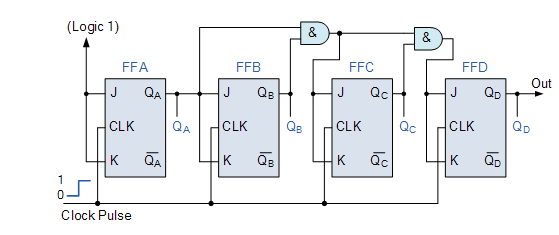
The external clock pulses (counting pulses) are fed directly to each of the J-K flip-flops in the counter chain, and both the J and K inputs are tied together in toggle mode, but only the first flip-flop, flip-flop FFA (LSB), is connected HIGH, logic “1,” allowing the flip-flop to toggle on every clock pulse. The synchronous counter then advances one state for each pulse in response to the common clock signal, following a specified sequence of states.
The J and K inputs of flip-flop FFB are directly connected to the output QA of flip-flop FFA, whereas the J and K inputs of flip-flops FFC and FFD are driven by separate AND gates that are likewise fed signals from the preceding stage's input and output. The appropriate logic for the JK inputs of the following stage is generated by these additional AND gates.
We can have the same counting sequence as the asynchronous circuit but without the ripple effect if we enable each JK flip-flop to toggle based on whether or not all previous flip-flop outputs (Q) are “HIGH,” because each flip-flop in this circuit will be timed at exactly the same time.
The maximum operating frequency of this type of frequency counter is substantially higher than that of a similar asynchronous counter circuit because synchronous counters have no inherent propagation delay because all counter stages are triggered in parallel at the same time.
4.14.2 4-bit Synchronous Counter Waveform Timing Diagram
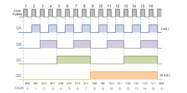
Because every clock pulse counts consecutively, the outputs of this 4-bit synchronous counter count upwards from 0 ( 0000 ) to 15. ( 1111 ). As a result, a 4-bit Synchronous Up Counter is another name for this type of counter.
However, by connecting the AND gates to the Q outputs of the flip-flops as indicated, we can simply build a 4-bit Synchronous Down Counter with a waveform timing diagram that is the inverse of the above. The counter starts with all of its outputs HIGH ( 1111 ), then counts down on each clock pulse until it reaches zero ( 0000 ), before repeating.
4.14.3 Binary 4-bit Synchronous Down Counter

Because synchronous counters are built by connecting flip-flops together, and any number of flip-flops can be connected or "cascaded" together to form a "divide-by-n" binary counter, the modulo's or "MOD" number still applies, allowing a Decade counter or BCD counter with counts ranging from 0 to 2n-1 to be built, as well as truncated sequences. An additional flip-flop and AND gate across an up or down synchronous counter is all that is required to raise the MOD count.
Decade 4-bit Synchronous Counter
To produce a count sequence from 0 to 9, a 4-bit decade synchronous counter can be made utilising synchronous binary counters. With the help of some additional circuitry, a regular binary counter can be turned to a decade (decimal 10) counter to accomplish the needed state sequence. The counter resets to “0000” after reaching the count of “1001”. We now have a decade counter, sometimes known as a Modulo-10 counter.
4.14.4 Decade 4-bit Synchronous Counter
When the counting sequence hits “1001,” (Binary 10) the additional AND gates detect it and force flip-flop FF3 to toggle on the next clock pulse. Every clock pulse toggles the flip-flop FF0. As a result, the count is reset to “0000” and a synchronous decade counter is created.
We could easily rearrange the additional AND gates in the above counter circuit to produce different count numbers, such as a Mod-12 counter that counts 12 states from “0000′′ to “1011” (0 to 11) and then repeats, making them appropriate for clocks and other applications.
Triggering A Synchronous Counter
When the clock input changes state, synchronous counters use edge-triggered flip-flops that change states on either the "positive-edge" (rising edge) or the "negative-edge" (falling edge) of the clock pulse on the control input, resulting in a single count.
In general, synchronous counters count on the rising-edge of the clock signal, which is the low to high transition, while asynchronous ripple counters count on the falling-edge of the clock signal, which is the high to low transition.

Although it may appear peculiar that ripple counters change state on the falling-edge of the clock cycle, this makes it easier to connect counters since the most significant bit (MSB) of one counter can control the clock input of the next.
Because the next bit must change state when the preceding bit changes from high to low — the point at which the following bit must be carried – this works. Synchronous counters often include a carry-out and carry-in pin for connecting counters without propagation delays.
Synchronous Counter Summary
Then, to summarise some of the key facts concerning Synchronous Counters, consider the following:
1. Toggle or D-type flip-flops can be used to create synchronised counters.
2. Asynchronous counters are more difficult to create than synchronised counters.
3. They're termed synchronous counters since the flip-flops' clock input is synchronised.
Having the same clock signal, are all timed together at the same time.
4. All output states switch or change at the same time as a result of this single clock pulse.
5. There is no intrinsic propagation delay when all clock inputs are linked together.
6. Because the clock is provided in parallel to all flip-flops, synchronous counters are also known as parallel counters.
7. The counter's current status is kept track of by the built-in memory circuit.
8. Logic gates are used to control the count sequence.
9. When compared to asynchronous counters, overall faster operation is possible.
Synchronous Up Counter

The basic Synchronous counter design is displayed in the following figure, which is a Synchronous up counter. A 4-bit synchronous up counter begins counting at 0 (0000 in binary) and increments or counts upwards to 15 (1111 in binary) before being reset to begin a new counting cycle. It has a substantially greater operating frequency than an Asynchronous counter in the same range. Also, because all flip-flops or counter stages are in parallel clock sources, the clock activates all counters at the same time, there is no propagation delay in the synchronous counter.
The external clock is delivered in parallel to all J-K Flip-flops at the same time. The first flip-flop, FFA, is coupled to a Logic 1 external input through J and K pins, which is the least significant bit in this 4-bit synchronous counter. HIGH logic across the Logic 1 signal, as a result of this connection, changes the state of the first flip-flop on every clock pulse.
The input pins of J and K are connected across the output of the first flip-flop in the next stage, the second flip-flop FFB. Two distinct AND gates provide the necessary logic spanning FFC and FFD in the case of FFC and FFD. Those AND gates use the input and output from the previous stage flip-flops to construct logic.
By generating a condition where each flip-flop changes its state dependent on whether or not all previous flip-flops output is HIGH in logic, we can build the identical counting sequence employed in the Asynchronous counter. However, because all flip-flops are clocked at the same time, there will be no ripple effect in this scenario.
Synchronous Down Counter

We may develop Synchronous Down Counter by making minor adjustments to the AND section and using the inverted output from the J-K flip-flop. A 4-bit synchronous down counter starts counting from 15 (1111 in binary) and decrements or counts downwards to 0 or 0000 before being reset and starting a new counting cycle. The AND Gate input is altered in the synchronous down counter. The first Flip-flop FFA input is identical to that of the prior Synchronous up counter. Instead of supplying the first flip-output flop's directly to the next flip-flop, we utilise an inverted output pin that gives J and K input across the following flip-FFB flop's and also serves as an input pin for the AND gate. Two AND gates, similar to the previous circuit, provide crucial logic to the next two Flip-flops FFC and FFD.
Synchronous Counter Timing Diagram

The clock input across flip-flops and the output timing diagram are depicted in the image above. Synchronous counter counts progressively on each clock pulse. For a 4-bit Synchronous up counter, the counting output over four output pins is incremental from 0 to 15, in binary 0000 to 1111. After the 15 or 1111, the counter is reset to 0 or 0000, and a new counting cycle begins.
When the inverted output is linked across the AND gate in a synchronous down counter, the counting step is reversed. The counter counts from 15 or 1111 to 0 or 0000 before being restarted to begin a new counting cycle, beginning at 15 or 0000.
4 bit-Synchronous Decade Counter
A Decade counter, sometimes known as a BCD counter, is produced by cascading flip-flops and can count from 0 to in the same way as an asynchronous counter. It will have a “divide by n” capability using modulo or MOD number, just as an asynchronous counter. The Synchronous counter's MOD count must be increased (can be in Up or Down configuration).
Here is the 4-bit Synchronous Decade counter circuit is shown-

The above circuit employs a Synchronous binary counter, which generates a count sequence ranging from 0 to 9. Additional logic is provided to achieve the necessary state sequence as well as to convert the binary counter to a decade counter (base 10 numbers, Decimal). The counter will reset to 0000 when the output hits count 9 or 1001, and then count up to 1001.
AND gates in the above circuit will detect when the counting sequence reaches 9 or 1001 and alter the state of the third flip-flop from the left, FFC, on the next clock pulse. The counter is then reset to 000 and the counting begins again until 1001 is reached.
If we modify the position of the AND gates in the above circuit, it will count 12 states from 0 (0000 in binary) to 11 (1011 in binary) and then reset to 0.
Trigger Pulse related information
Positive edge and Negative edge flip-flops are the two types of edge triggered flip-flops available.
When the clock input changes from Logic 0 to Logic 1, or Logic Low to Logic High, Positive Edge or Rising Edge flip-flops count one single step.
Negative Edge or falling Edge flip-flops, on the other hand, count one step when the clock input goes from Logic 1 to Logic 0, or Logic High to Logic Low.

To change state, ripple counters use falling edge or negative edge induced clock pluses. There's a reason for this. It will be easier to cascade counters together since one counter's Most Significant bit can control the clock input of the following counter.
For counter linking applications, synchronised counters provide carry out and carry in pins. There is no propagation delay inside the circuitry as a result of this.
Use of Synchronous Counter
Few applications where Synchronous counters are used-
- Machine Motion control
- Motor RPM counter
- Rotary Shaft Encoders
- Digital clock or pulse generators.
- Digital Watch and Alarm systems.
4.14.5 Different types of Synchronous Counters
There are many types of synchronous counters available in digital electronics. They are listed below.
- Binary counters
- 4 bit synchronous UP counter
- 4 bit synchronous DOWN counter
- 4 bit synchronous UP / DOWN counter
- Loadable counters
- BCD counters
- Ring counters
- Johnson counters etc.
4 bit Synchronous UP Counter
The JK flip flop is used to create the four-bit up counter depicted in the diagram below. All of the flip flops are wired in parallel to an external clock pulse.
JK flip flop is recommended for counter design.
The importance of employing a JK flip flop is that it can toggle its state depending on the clock pulse if both inputs are high.
The first flip flop's inputs are linked to HIGH (logic 1), causing the flip flop to toggle for each clock pulse input. As a result, the synchronous counter will operate with a single clock signal and will change state with each pulse.
The input of the second flip flop is connected to the output of the first JK flip flop (Q). The inputs of the other two flip flops are driven by the AND gates (which are connected outside). The AND gates' inputs come from the preceding stage's lip flop outputs.
The counter would not function properly if the inputs of FF2 were linked directly to the Q1 output of FF1. This is because at count of 210, the Q1 value is high, indicating that the FF2 flip flop will toggle for the third clock pulse. As a result, the counting operation is incorrect, and the count is 710 instead of 410.
AND gates are utilised on the input side of FF2 and FF3 to avoid this problem. Only when the Q0 and Q1 outputs are both high will the AND gate's output be high. As a result, the count for the following clock pulse will be 00012.
When Q0, Q1, and Q2 are all high, the flip flop FF3 will toggle for the fourth clock pulse. The Q3 output will not toggle until the eighth clock pulse, after which it will remain high until the sixteenth clock pulse. The q outputs of all flip flops will revert to zero after the 16th clock pulse.
Operation
The 4 bit binary sequence in the up counter starts at 0000 and advances up to 1111. Know about JK Flip flop before knowing how the above up counter circuit works.
The two inputs of the flip flop are linked together in the above circuit. As a result, there are only two conceivable outcomes, namely, either the two inputs are high or low.
If both inputs are high, the JK flip-flop toggles; if both inputs are low, the JK flip-flop recalls the prior state.
Let's have a look at the procedure. The term "clock pulse" refers to a clock pulse that is triggered by an edge.
1.) All of the flip flops' outputs will be at 0000 during the first clock pulse.
2.)As the inputs of J and k are linked to the logic high in the second clock pulse, the output of the JK flip flop (FF0) changes state.
As a result, the state of the first flip-output flop's (FF0) changes with each clock pulse.
This can be seen in the sequence described above.
Alternately, the LSB alters its state. As a result, -0001 is produced.
3.) The next flip flop (FF1) receives its J K inputs (logic high) on the third clock pulse and changes its state. FF0 will alter its status to 0 at this point. As a result, the FF1's input is 0. As a result, the output is -0010.
4.) FF1 will not change its state in the fourth clock pulse since its inputs are in the low state; it will remain in the prior state. Despite the fact that it produces an output to FF2, the AND gate prevents it from changing its state. FF0 will toggle its output to the logic high state once more. As a result, the output is 0011.
5.) FF2 receives the inputs and changes its state on the fifth clock pulse. While FF0's output will be low logic, and FF1's will be low state, creating 0100.
This procedure continued until 1111.
The table below explains how things work. The above-mentioned synchronous counter's operation is detailed in the table below.
The outputs of four flip flops, Q1, Q2, Q3, and Q4, are shown in the table below. Pulse was initiated by the first flip-flop toggles on either edge. The second, on the other hand, is only triggered if its inputs are high at a certain clock pulse. If the two outputs Q1 and Q2 are both high, the third flip-flop toggles. Similarly, if all three Q1,Q2,Q3 are high, Q4 will toggle.
After reaching zero, the three flip flips toggle to logic low, 0000, and the count begins all over again.
Timing diagram for up counter is shown below.

4 bit Synchronous DOWN Counter
The numbers are counted in decreasing order by the down counter. This is comparable to an up counter, but the count should be reduced. As a result, the inverted Q (Q') is connected to the inputs of the JK flip-flop. The JK flip flop is used to create the four-bit down counter depicted in the diagram below. All of the flip flops are connected to the same external clock pulse.
Due to the fact that the counter must count down the sequence, all of the inputs will be in a high state at first. Similar to the up counter, it will begin with 1111 and terminate with 0000.
It's important to remember that in the down counter, the previous flip flop will toggle only if the front flip flop produces low logic at its output.
4 bit Synchronous Up/Down Counter
The two counters mentioned above can be combined into a single counter called up down counter. This can be chosen from the available options. Below is a design for an up/down counter using JK flip flops.

The up/down counter has two count modes: “Up” and “Down.” It contains two input AND gates that identify the required bit conditions for counting. OR gates are used to merge the outputs of each JK flip flop's AND gate.
We give an up/down control line that allows the outputs of JK flip flops, Q, Q', to be passed to the next level of the cascaded arrangement via an upper or lower series of AND gates.
The top AND gates are enabled and the circuit works as a UP counter when the up/down control line is set to HIGH. The bottom AND gates are enabled when the up/down control line is set to low, and the circuit operates as a DOWN counter.
Applications of Synchronous Counters
Machine motion control, in which rotary shaft encoders convert mechanical pulses into electric pulses, is the most prevalent and well-known application of synchronous counters. These pulses will operate as the up/down counter's clock input, causing the circuit to move.
A photo transistor or light sensor is attached to the rotor shaft in this circuit. This configuration is linked to the UP/DOWN counter. When the machine starts moving, it connects and disturbs (makes and breaks) the light beam between the light sensor and the LED, which rotates the encoder shaft.
The rotor generates clock pulses as a result of this motion, increasing the count of the up/down counter circuit. As a result, the counter note records the motion of the shaft and calculates the distance travelled by the rotor.
We increment the count by moving the rotor shaft in one direction and decrease the count by moving the shaft in the opposite direction to count the motion of the rotor shaft. To distinguish the direction of motion, we additionally need an encoder/decoder circuit.
Key takeaway:
- In the diagram above, a 4 bit asynchronous DOWN counter is displayed. The UP counter can be easily modified. The DOWN counter is a four-bit counter that counts numbers from 15 to 0 downwards.
- The clock signal input to the remaining flip flops in the counter is taken from Q output of the previous flip flop, rather than Q' output.
References:
1. The Art of Electronics by Paul Horowitz and Wilfield Hill, Cambridge University -2006
2. Electronics by Allan R. Hambley, Prentice Hall - 1994
3. Digital Logic and Computer design M. Morris Mano (Pearson) -2016
4. Concepts of Electronics D.C. Tayal (Himalaya Publishing house) -2018