Unit - 1
Integrated Circuits and Digital Circuits
1.1.1 What are Active Components?
Active components are devices that can amplify and produce power from an electric signal. An oscillator, transistor, or integrated circuit will be present in any typical active component. In devices, an active component serves as an alternating current circuit. This aids the device's ability to increase power and voltage. Because it is fueled by electricity, this component can carry out its functions. All active components require a source of energy, which is typically derived from a DC circuit.
Example of Active Components
Because of their nature, active components rely on external sources to function. They have the ability to supplement and provide power to the circuit. The many sorts of active components are listed below.
Transistors:
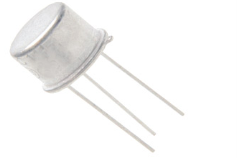
Transistors magnify current by taking in a low voltage of energy and producing a higher output voltage. This semiconductor device is a crucial component that can be found in a variety of circuit designs. BC547, 2N2222, and BC557 are the most popular and widely used transistors. Depending on the device's planning, they can be individualistic or packaged together. The most often used Transistors have a wide range of functions, including voltage regulation, amplification, signal adjustment, and so on.

Silicon Controlled Rectifiers (SCRs):
SCRs, or Silicon Controlled Rectifiers, are a form of power electronics switch. Anode, Cathode, and Gate are the three terminals. The switch is open by default, and no current flows between the SCR's anode and cathode terminals. The switch is closed when a tiny current is applied to the gate pin, allowing a considerable amount of current to travel between the Anode and Cathode terminals. The operation of a Thyristor/SCR is similar to that of a BJT (Transistor). The load to be switched is connected between the anode and cathode, and the Thyristor is turned on or off by passing a gate current through the gate pin. 2N2324 and 2N1595 are the most popular and widely used Thyristors.
1.1.2 What are Passive components?
A second electrical signal cannot be used to control electric current in passive components. Capacitors, resistors, inductors, and transformers are all crucial passive components. With the exception of the AC circuit, passive components do not require energy to operate. They are unable to increase the signal power or amplify it, unlike the Active component. Passive components are divided into two categories.
Lossy or Dissipative: These can't take power from a separate circuit. Lossy passive components, such as resistors, are one example.
Lossless: There is no net level flow of input or output in them. Inductors, transformers, and gyrators are examples of lossless components.
The majority of passive components have two terminals, which are referred to as two-port terminals. They usually follow the rules of reciprocity. Transistors and electronic filters are examples of two-port networks. Circuit architecture, such as resistors, inductors, voltage, and current sources, are used by some passive components.
Examples of Passive Components
Passive components, on the other hand, do not require any external source of energy to operate. They distribute energy across the circuit. The following is a list of the most common passive components.
Capacitors:
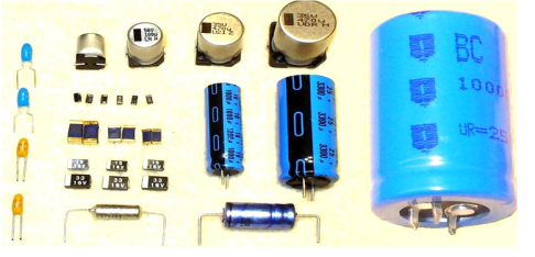
The electric field between plates can be used to store energy in capacitors. They're often utilised for storing in electronic circuits. They can also be used to distinguish between high and low-frequency signals in filter circuits. Ceramic capacitors, electrolytic capacitors, mylar capacitors, and X-rated capacitors are the most common types of capacitors. You can also read this article on Capacitors to learn about the fundamentals of capacitors, their types, and their applications.
Resistors:
Their job is to resist or oppose the passage of current, as the name implies. They are designed to regulate the flow of electric current in a circuit by lowering the voltage in the device. You can also read this Resistors page to learn about the fundamentals of resistors, their types, and applications.

Inductors:
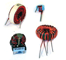
They can also be utilised to store and transmit energy. Inductors have a very high impedance on AC and a very low impedance on DC within the limitations of a circuit. Inductors are widely used in power supply circuits such as AC/DC converters, SMPS circuits, and so on. You can also read this article on inductors to learn about the basics, types, and applications of inductors.
Diodes:
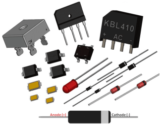
Diodes are small active components that direct the flow of energy inside the circuit's boundaries. The diode's role is critical because it regulates energy flow, preventing harm from occurring as a result of insufficient energy flow. 1N4007 Rectifier Diode, 1N4732A 4.7V Zener Diode, and 1N5817 Schottky Diode are the most popular and widely used diodes. You may learn more about the basics of diodes, their types, and properties by reading this Diode Article.
1.1.3 Differences between Active and passive components
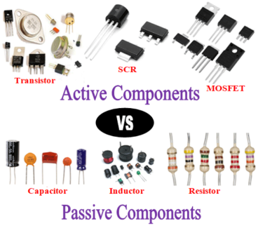
All electronic components can be divided into two categories: active components and passive components. Based on their functional features and functioning, these components are diametrically opposed to one another. We'll learn about the many sorts of active and passive components, as well as the differences between active and passive devices, in this post. But, before understanding how different they are from each other, it is important to understand what each component means and how they work, so let's get started with active components.
Now that we have understood about the Active and Passive devices and its types, let us do a comparison between active and passive components based on certain parameters as defined below
1) Source of energy – Active components necessitate an additional energy source. The operation of passive components does not necessitate the use of an additional source of energy. A resistor is self-contained and does not require a certain voltage to function.
2) Energy: Active components produce energy in the form of voltage or current, whilst passive components, such as a capacitor, store energy in the form of an electric field and an inductor, store energy in the form of a magnetic field.
3) Linearity: Active components are non-linear, whereas passive components are linear. According to Ohms Law, the voltage drop across a passive component like a resistor will be linear to its resistance value. The output of a transistor or other active component, on the other hand, will have a non-linear amplification factor.
4) Power gain: Active components can provide power growth, however passive components lack the potential to magnify power.
5) Controlling the current: As the name implies, an active component may easily influence current flow. A passive component cannot do the same task.
6) External source: Active components, as previously said, require an additional source to control and sustain their activities, whereas passive components do not require an external source.
1.1.4 Comparison Chart
BASIS | ACTIVE COMPONENTS | PASSIVE COMPONENT |
Nature of source | The circuit receives electricity or energy from active components. | Passive elements make use of the circuit's power or energy. |
Examples | Diodes, transistors, SCRs, integrated circuits, and other electronic components | Resistor, capacitor, inductor, and other electronic components |
Function of the component | Devices that generate voltage or current as a kind of energy. | Energy is stored in the form of voltage or current in these devices. |
Power Gain | They have the ability to increase power. | They aren't capable of gaining authority. |
Flow of current | The flow of current can be controlled by active components. | The flow of current cannot be controlled by passive components. |
Requirement of external source | They need to get their operations from somewhere else. | The operations do not necessitate the use of any external resources. |
Nature of energy | Energy is provided by active components. | Energy acceptors are passive components. |
In this article, the difference between active and passive components is discussed in detail. The elements or gadgets that are capable of providing or distributing energy to the circuit are known as active components. Passive components are the ones that do not require any external source for the operation and are capable of storing energy in the form of voltage or current in the circuit.
Key takeaway:
- A little chip called an integrated circuit, or IC, can be used as an amplifier, oscillator, timer, microprocessor, or even computer memory. An integrated circuit (IC) is a compact silicon wafer that can contain hundreds to millions of transistors, resistors, and capacitors. The final ITRS was published in 2016, and the International Roadmap for Devices and Systems has taken its place. ICs were originally just electronic devices. Because of the success of integrated circuits, additional technologies have been integrated in an attempt to achieve the same advantages of compact size and low cost.
1.2.1 Integrated circuit (IC)
An integrated circuit (IC) consists of a single - crystal chip of silicon, containing both active (diodes and transistors) and passive (resistors, capacitors) elements and their interconnections. The following are some of the advantages of integrated circuits versus discrete components:
(i) Extremely small in size
(ii) Low power consumption
(iii) Reliability
(iv) Reduced cost
(v) Very small weight
(vi) Easy replacement
Digital ICs and linear ICs* are two types of integrated circuits that have a wide range of applications. Monolithic and hybrid IC technologies were used, which are two very different IC technologies.
All active and passive circuit components, as well as their interconnections, are built on top of a single silicon chip in monolithic integrated circuits. The monolithic circuit is appropriate for circumstances where identical currents must be received in huge quantities. As a result, it has the lowest cost per unit and the best level of reliability. Separate component pieces are mounted to a ceramic substrate in hybrid circuits, and the components are joined using either metallization patterns or wire bonding.
Typical chip sizes range from around 40 mils (0.001 inch) to around 300 mils (0.001 inch), depending on the circuit complexity. On a single chip, any number of components from a few to thousands can be manufactured. Dual-in-line packages are available for the integrated circuits (DIP).
1.2.2 Semiconductor devices
Semiconductor Devices – A semiconductor substance is a material that permits electric current to pass through it. Consider the CPU device: it contains a large number of transistors, each of which contains semiconductor material that permits current to flow, and all of these are controlled by a switch. The passage of electric current is regulated by actions dependent on the status of the switch, whether it is on or off, in this case a transistor. As a result, a Semiconductor Device is a device that permits electricity to pass through it partially.
Examples of Semiconductor Devices
The moniker "Semi Conductors" comes from the fact that these devices are neither good insulators nor good conductors. The following are some examples of semiconductors:
- Op-amps (operational amplifiers)
- Ohm resistors
- Capacitors are a type of capacitor.
- Diodes are light-emitting diodes.
- Transistors are a type of semiconductor.
Because of their dependability, compactness, and low cost, these devices are frequently employed in a variety of applications. A semiconductor is a discrete component that is utilised in optical sensors, power devices, light emitters, and solid-state lasers. They also offer a wide range of current and voltage handling capacities, with current ratings ranging from a few nano-amperes (109 ampere) to more than 5,000 voltage and ampere ratings, with voltage levels exceeding 100,000 volts.
Semiconductor devices are self-contained in their ability to integrate into complicated circuits and are easily manufactured into microelectronic circuits. They also have a bright future as critical components in a wide range of electrical and electronic instruments and systems, including communications, data processing, consumer electronics, and industrial control equipment.
1.2.3 Types of Semiconductor Devices
These devices are classed as two-terminal, three-terminal, or terminal devices, depending on their configuration. Diode, Zener diode, Laser diode, Schottky diode, Light-emitting diode (LED), Photocell, Phototransistor, Solar cell, and other two-terminal devices are examples.
Bipolar transistors, IGBTs, Field-effect transistors, Silicon-controlled rectifiers, TRIACs, and Thyristors are examples of three-terminal semiconductor devices.
1.2.4 Applications of Semiconductor Devices
- They're employed in the design of logic gates and digital circuits, which are found in microprocessors, as well as analogue circuits like oscillators and amplifiers.
- In high-voltage applications, this component is used.
1.2.5 Diode
A diode is a semiconductor device with only one p-n junction. P-n junctions are made by connecting p-type and n-type semiconductor materials together. This formation is due to the reason that the n-type region has a higher number of electron concentrations whereas the p-type region has a higher number of hole concentrations, hence, the electrons get diffused from the n-type region to the p-type region. As a result, this phenomenon is employed in the production of light.
1.2.4 Transistors
Bipolar junction transistors and field-effect transistors are the two types of transistors. The development of two p-n junctions in two different configurations, such as n-p-n or p-n-p, results in a bipolar junction transistor. The three regions formed in this sort of transistor are known as the emitter, collector, and base or middle region.
The field-effect transistor works on the basis of conductivity, and the presence of an electric field can change the conductivity.
1.2.5 Basic logic gates using discrete components
Logic gates
Logic gates are circuits that are used to process digital signals. They have a binary nature to them. A gate is a single-output digital circuit with one or more inputs. Only particular combinations of input logic levels result in the output. Most digital systems are constructed using logic gates as the basic building pieces. A logic circuit's two potential states are represented by the numbers 0 and 1. The two states can also be referred to as 'ON and OFF' or 'HIGH and LOW' or 'TRUE and FALSE'.
Basic logic gates using discrete components
'OR', 'AND', and 'NOT' gates are the essential components of a digital system. The simplest logic gates are these three gates. A table called TRUTH TABLE represents all of a logic circuit's possible inputs and outputs. The basic gates' functions are demonstrated using circuits and truth tables in the following sections.
(i) OR gate
There are two or more inputs but only one output in an OR gate. Because the output is high if any or all of the inputs are high, it's called an OR gate. Figure a shows the logic symbol for a two-input OR gate.
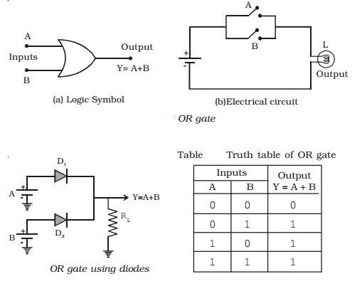
Y= A+B (+ symbol should be read as OR) is the Boolean expression for the OR gate.
The OR gate can be compared to the electrical circuit depicted in Fig. b, in which switches are connected in parallel. If any or both of the inputs are closed, the lamp will light up.
Diode OR gate
The diagram depicts a basic circuit that uses diodes to create a two-input OR gate. This circuit's operation can be explained as follows.
Case (i) A = 0 and B = 0
Because the diodes are non-conducting, the output voltage will be low when both A and B are at zero, (i.e.) low.
Case (ii) A = 0 and B = 1
Diode D2 is forward biassed when A is low and B is high, allowing current to flow through RL and a high output.
Case (iii) A = 1 and B = 0
When A is high and B is low, diode D1 conducts and the output is high.
Case (iv) A = 1 and B = 1
When A and B both are high, both diodes D1 and D2 are conducting and the output is high. As a result, Y is high. Table shows the OR gate operations.
(ii) AND gate
There are two or more inputs but only one output in an AND gate. Because the output is high only when all of the inputs are high, it's called an AND gate. Figure a shows the logic symbol for a two-input AND gate.
(should be read as AND) Y = AB
The AND gate can be thought of as an electrical circuit in which the switches are connected in series, as shown in Fig. b. The bulb will only light up if A and B are both closed, and the output will be high.
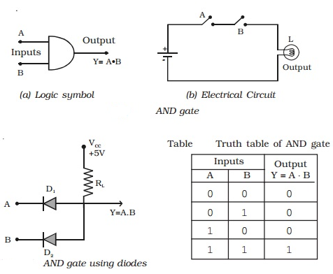
Diode AND gate
The diagram depicts a basic circuit for creating a two-input AND gate using diodes. The circuit's operation can be summarised as follows:
Case (i) A = 0 and B = 0
When A and B are zero, both diodes are in forward bias condition and they conduct and hence the output will be zero, because the supply voltage VCC will be dropped across RL only. As a result, Y = 0.
Case (ii) A = 0 and B = 1
Diode D1 is forward biassed and diode D2 is reverse biassed when A = 0 and B is high. Due to forward biassing, the diode D1 will now conduct. As a result, output Y = 0.
Case (iii) A = 1 and B = 0
In this case, diode D2 will be conducting and hence the output Y = 0.
Case (iv) A = 1 and B = 1
Both diodes are not conducting in this scenario. No current flows through RL since D1 and D2 are both turned off. The output voltage is the same as the input voltage. As a result, Y = 1.
As a result, the output will only be high when the inputs A and B are both high. The function of an AND gate is summarised in Table.
(iii) NOT gate (Inverter)
The NOT gate is a single-input, single-output gate. It gets its name from the fact that its output is a complement to the input. Inverter is another name for it. The logic sign for the NOT gate is shown in Fig. a.
The NOT operation is represented by the Boolean formula Y = A.
As shown in Fig. b, the NOT gate can be thought of as an electrical circuit. When switch A is closed, the input is high and the bulb does not light up (the output is low), and vice versa.
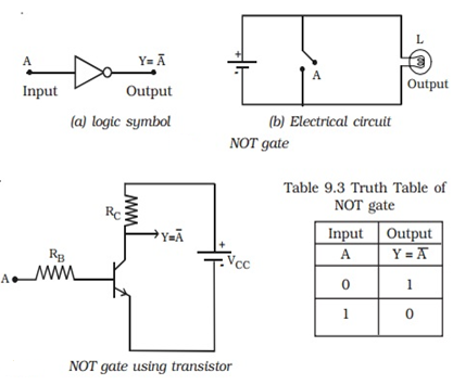
A transistor in CE mode is employed as a NOT gate in Fig. The transistor is forced into saturation when the input A is high, resulting in a low output Y. The transistor is in cutoff when A is low, hence the output Y is high. As a result, it can be seen that when input is high, output is low, and vice versa. Table depicts the operation of the NOT gate.
Exclusive OR gate (EXOR gate)
The logic symbol for exclusive OR (EXOR) gate is shown in
The Boolean expression to represent EXOR operation is
Y = A ⊕ B
EXOR gate has an output 1, only when the inputs are complement to each other.
The equivalent switching circuit is shown in Fig b.

Switch positions A and B will individually make the lamp to be ON. The combination of A and B, on the other hand, is not feasible.
Table shows how the EXOR procedure works.
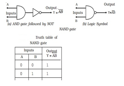
NAND gate
A NOT-AND gate is a gate that does not allow two things to happen at the same time. It can be obtained by connecting a NOT gate to an AND gate's output (Fig a).
Fig. b shows the logic sign for the NAND gate.
The NAND gate function is the polar opposite of the AND gate function. There will be an output from a NAND gate.
Only if neither of the inputs is 1. In other words, if either A or B, or both, are 0, the output is 1. 'The'
Table depicts the operation of a NAND gate.
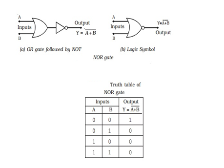
NOR gate
This is a gate with a NOT-OR condition. By connecting an inverter to the output of an OR gate, it can be created (Fig a).
Figure b shows the logic sign for the NOR gate.
The NOR gate function is the polar opposite of the OR gate. Only when all inputs are 0 will a NOR gate produce an output. When all inputs are low, the output of a NOR gate is high. Table shows how the NOR operation works.
Key takeaway:
- In solid-state electronic circuits, discrete resistors are commonly rated at 1/10, 1/8, or 1/4 watt. They normally consume less than a watt of electricity and don't need to be concerned about their power rating.
- A discrete semiconductor has a single basic function that cannot be separated into any other. An IC, for example, may contain a transistor, a diode, and other components that can each perform a different function on their own or, when used together as a circuit, can do multiple purposes.
1.3.1 What is an Integrated Circuit (IC)?
Previously, circuits were huge and cumbersome, consisting of circuit components such as resistors, capacitors, inductors, transistors, diodes, and other components coupled with copper wires. This aspect limited the circuits' application to large machinery. With these large circuits, it was impossible to make small and compact appliances. Furthermore, they were not completely shockproof or dependable.
Necessity, as they say, is the mother of all inventions. As a result, smaller circuits with more power and safety were needed to be integrated into gadgets. Three American scientists invented transistors, which greatly simplified things, but the creation of integrated circuits completely transformed the face of electronics technology.
The integrated circuit is a basic concept in electronics that draws on other key concepts we've already covered in class. As a result, read the following articles for a quick reference:
- Electric Circuits
- Resistors
- Transistors
- Diodes
- Capacitors
1.3.2 Definition of Integrated Chip
An integrated circuit, often known as an IC, is a compact semiconductor chip that contains a whole circuit. When compared to ordinary circuits, which are built up of distinct circuit components, it is extremely compact. Monolithic integrated circuits are the most frequent type of IC.
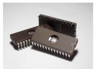
An Integrated Circuit (IC) is a microchip that contains thousands or hundreds of electrical components such as resistors, capacitors, and transistors. Oscillators, amplifiers, microprocessors, timers, and computer memory are all examples of ICs.
1.3.3 Integrated Circuit Design
Certain logic techniques and circuit designs are used to design an integrated circuit. Following are the two categories of IC design:
- Analog Design
- Digital Design
- Mixed Design
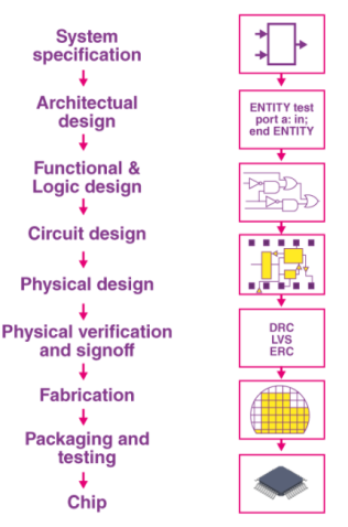
The digital design method is used to create ICs that are used as computer memories (such as RAM and ROM). This style of design ensures that the circuit density and overall efficiency are maximised. This approach is used to develop ICs that work with binary input data such as 0 and 1. The steps involved in creating digital integrated circuits are depicted in the diagram below.
Digital Design
Analog Design
The analogue design process is used to build integrated chips that are utilised as oscillators, filters, and regulators. When power dissipation, gain, and resistance must be ideal, this design method is utilised.
Mixed Design
The analogue and digital design ideas are combined in mixed design. Digital to Analog converters, Analog to Digital converters (D/A and A/D converters), and clock/timing ICs are all included in the mixed ICs.
Integrated Circuit Construction
A complicated layering of semiconductors, coppers, and other associated materials forms resistors, transistors, and other components in an integrated circuit. A die is a combination of these wafers that has been sliced and moulded.
The ICs' semiconductor wafers are delicate, and the connections between the layers are extremely complex. The ICs are packaged because the IC die is too small to solder and connect to. The IC package transforms the delicate and small die into a familiar black chip.
The integrated circuit is encased in an IC package, which transforms it into a device that can be easily connected. As illustrated in the diagram, there are many distinct sorts of packages, each with its own size and mounting options.
All integrated circuits (ICs) are polarised, and each pin in an IC has its own position and function. As seen in the diagram below, integrated chips employ a notch or a dot to denote the first pin.
Following the identification of the first pin, the subsequent PINs grow in counterclockwise order around the chip.
1.3.4 Integrated Circuit Features
Construction & Packaging
Semiconducting materials, such as silicon, are used to make integrated circuits. Because the integrated chip is so small and delicate, it is attached to a set of tiny gold and aluminium wires before being moulded into a flat block of plastic or ceramic. Metal pins on the outside of the block connect to the wires inside. The solid block keeps the chip cold and protects it from overheating.
Size of an IC
The integrated chip's size ranges from 1 square mm to more than 200 mm.
Integration of an IC
Integrated chips receive their name from the fact that they combine multiple devices on a single chip. A microcontroller is an integrated circuit (IC) that combines a microprocessor, memory, and interface into one device.
1.3.5 Commonly Used ICs
Logic Gate ICs
Logic gate integrated circuits (ICs) are combinational circuits that provide a logical output from a variety of input signals. Two to three inputs are possible, but only one output is possible.
Timer ICs
A Timer IC is made with precise timing cycles and a duty cycle of either 100% or 50%.
Operational Amplifiers
An OpAmp, or Operational Amplifier, is a voltage amplifier with a high gain and a single-ended output that has a differential input.
Voltage Regulators
A voltage regulator IC maintains a steady DC output regardless of the DC input.
1.3.6 Mica and Single Crystal Substrates, Silicon Chip Specimen, Supports and Wafers, Gold Coated Silicon Wafers, Slides and Coverslips
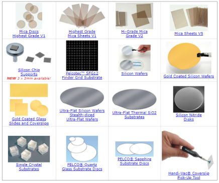
Mica substrates for afm, tem and sem:
Surfaces of newly cleaved muscovite mica have an exceptional evenness, are optically flat, clear, transparent, scratchless, and fingerprint-free. They're great for carbon support film creation, particle imaging, cell growth, and thin film coating research in electron microscopy. Surfaces of muscovite mica can also be used as substrates for high-resolution atomic force microscopy studies of dna, dna-protein, and thin films.
Cleaving mica entails carefully prying apart the leaves using a sharp edge or point inserted into an edge or corner of the sheet. A sharp razor blade edge will suffice, and in other circumstances, a sharp pointed tweezer would suffice. To take advantage of the clean and even surface, use the freshly revealed micro surface right after cleaving. Die-cut muscovite mica is available in a variety of sizes. Mica sheets range in thickness from 0.18 to 0.25mm (0.007 to 0.01"), resulting in much thinner, more homogeneous sheets.
Cleaving can also be accomplished by applying a double-coated piece of tape to the mica surface and gently pulling the mica layer away from one edge. Then, with the tape side down, lay mica on a specimen disc or mount. On the 001 plane, muscovite mica cleaves. Ruby muscovite comes in a variety of colours, from virtually white to pink to light ruby to brownish ruby and brown. It has a greater grade than green muscovite due to its hardness and outstanding cleavage capabilities, which allow it to be divided into the thinnest desired film without splitting. It has a flat optical surface, is robust, and is incompressible. Even at high temperatures, it stays robust and elastic while splitting into thin films along its cleavage planes. Mica is a complex hydrous aluminium silicate including potassium, magnesium, iron, sodium fluoride, and/or lithium, as well as trace amounts of other metals. Water, acids (excluding hydrofluoric and strong sulfuric acids), alkalis, common solvents, and oil are all stable and inert to it. Our mica is free of inclusions, air and bubbles, and is completely clean. Mica grading criteria are described in ASTM D-351.
Mica Grade V1 Properties and Chemical Composition
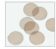
AFM Mica Discs
Grade V1 mica is 0.21mm (0.0085”) thick and of the highest quality. 10 packages of interleave It's possible to mount it on AFM/STM CDs.
Available in four diameters:
10mm (0.39")
12mm (0.47")
15mm (0.59")
20mm (0.79")
| |||||||||||||||||||||||||||||||||||||
Highest Grade Mica Sheets Highest quality Grade V1 0.15 to 0.177mm (0.006 - 0.007") thick Sheets interleaved Various sizes 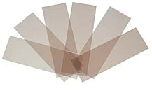
| |||||||||||||||||||||||||||||||||||||
|
| ||||||||||||||||||||||||||||||||||||
Hi-Grade Mica Grade V2 0.23 to 0.3mm (0.009 - 0.012") thick Sheets interleaved Various sizes 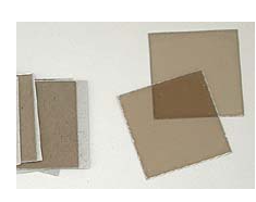
|
| ||||||||||||||||||||||||||||||||||||
|
| ||||||||||||||||||||||||||||||||||||
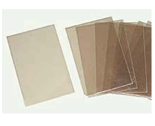
PELCO® Mica Sheets, Grade V5 Various sizes available, presenting many fresh, clean surfaces for such EM applications as carbon filming and particle spraying. Thickness, 0.23mm - 0.3mm (0.009" - 0.12").
|
| ||||||||||||||||||||||||||||||||||||
|
| ||||||||||||||||||||||||||||||||||||
Handi-Vac® Coverslip Pick-Up Tool
To pick up coverslips, mica, and Si chips, use this hand-operated vacuum pump with a 1/2" straight tip and a 9.3mm (3/8") silicone cup.
- Rubber body is ESD safe and can pick up and hold up to 35g.
- Picks up cover glasses, mica, or silicon discs with ease for precise placement.
- Silicone rubber cup with no scratches
- Tweezers that are more user-friendly than traditional metal tweezers

|
Silicon Chip Specimen Supports
Specimen supports with a low backdrop for SEM viewing
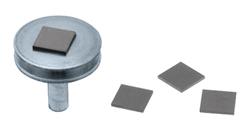
Si-chips are transparent, have a low electrical resistance, and have glass-like surface characteristics (including smoothness). They can also be used as a growing or mounting surface for cells. Before being packaged, Si-chips are cleaned. Due to the minimal background signal, it's also great for imaging minuscule particles.
Availability: 4" wafer (#16010) is precut into 3 x 3mm, 5 x 7mmm, 5 x 5mm, 10 x 10mm, 20 x 20 mm or 20 x 30mm chips that can be easily separated in the laboratory.
- BRAND NEW 4 "4" wafer precut into 5 x 7mm chips approximately 187 chips/wafer 4" wafer precut into 5 x 5mm chips approximately 270 chips/wafer wafer precut into 3 x 3mm chips approximately 600 chips/wafer wafer precut into 3 x 3mm chips approximately 600 chips/wafer wafer precut into 3 x 3mm chips approximately 600 chips/wafer wafer precut into 3 x 3mm chips approximately 600 chips/wa
- (4) "pre-cut wafer into 10 x 10mm chips about 55 chips per wafer
- (4) "wafers that have been precut into 20 x 20mm chips about ten chips per wafer
- (4) "Wafers are precut into 20 x 30mm chips, with 6 chips per wafer.
Characteristics:
- Orientation:
- 1-30 Ohms of resistance
- P (Boron) is the type (1 primary flat)
- There is no SiO2 top coating.
- 18-21 mil (460-530m) wafer thickness
- One side of the wafer is polished.
- 2 nm roughness
- They are cleaned by rinsing them in de-ionized water before dicing.
| |||||||||||||||||||||||||||||||||||||||||
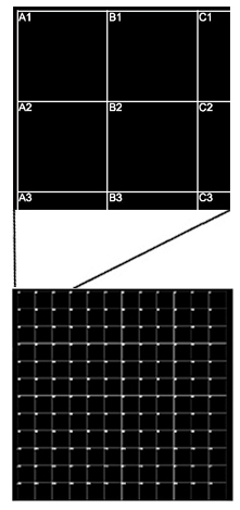
Pelcotec SFG12 Finder Grid Substrate A flat, conductive silicon substrate with a die size of 12.5 x 12.5mm, the PelcotecTM SFG12 finder grid substrate is a new PelcotecTM product. A 1 x 1mm raster is used to cover it, yielding a total of 12x12=144 fields. Each field has its own label, which follows an alphanumeric pattern. The lines and labels are laser etched into the silicon surface with great precision. It's the ideal compromise between a flat specimen support and a SEM finder grid. This unusual and creative product resembles an engraved SEM specimen mount in appearance, but it offers a variety of extra benefits: Flat - unlike copper finder grids, there are no height discrepancies. Detailed pattern across a vast region - more so than etched SEM mounts Low background signal - identical to Si chip substrates Only one element (Si) from the finder substrate was used for EDX investigation. 1mm spacing with 144 fields makes it practical and easy to navigate. The pattern can be seen with the naked eye, a preparation microscopy, and a scanning electron microscope (SEM). At (very) low magnification, it gives an approximate size. Easily placed on SEM sample stubs - compatible with the majority of common sizes SEM, FIB, XPS/ESCA, Auger, and LM can all be employed. The silicon substrate utilised had the following specifications: prime virgin silicon wafer, P Boron doped, 100> orientation, resistivity of 0.5-35 ohm/cm, thickness 645 m 55 m. |
Prod # | Description | Unit | Price | Order / Quote | |
21480 | Pelcotec™ Silicon SFG12 Finder Grid Substrate | Each | $19.75 |
|
1", 2", 3", 4" and 6" Silicon Wafers
These 1", 2", 3", 4" and 6" diameter silicon wafers can be used either as a substrate for thin film research or to make small silicon substrates by dicing the wafer into smaller pieces using a scriber and the Wafer Cleaving / Glass Breaking Pliers. The wafer is shipped in a wafer carrier.
Wafer Mounting Film
Properties:
- Orientation: 1 for 100> "111> for 3" Resistance: 1-30 Ohms, 2", 4", and 6" wafers
- (Boron) Type P: (1 primary flat)
- There is no SiO2 top coating.
- The thickness of a wafer is measured in millimetres.
- A single "= 10 - 12 millimetres (254 - 304 metres)
- A second "= 9 - 13 millimetres (230 - 330 metres)
- A third "= 13.6 – 18.5 millimetres (345 – 470 metres)
- (4) "= 18.7 – 22.6 millimetres (475 – 575 metres)
- (6) "= 23.6 – 25.2 millimetres (600 – 690 metres)
- 2 nm roughness
- TTV: 20m TTV: 20m TTV: 20m TTV: 20m TTV: 20m TTV: 20
- One side of the wafer is polished.
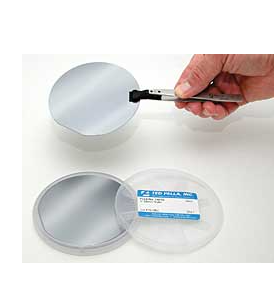
| 1", 2", 3", 4" and 6" Silicon Wafers These silicon wafers with diameters of 1", 2", 3", 4", and 6" can be used as a thin film research substrate or to manufacture miniature silicon substrates by dicing the wafer into smaller pieces with a scriber and the Wafer Cleaving / Glass Breaking Pliers. A wafer carrier is used to transport the wafer. Mounting Film for Wafers
Characteristics:
| |||||||||||||||||||||||||||||||||||||||||||||||||||
| ||||||||||||||||||||||||||||||||||||||||||||||||||||
Ultra-Flat 4" Silicon Wafers
4 Ultra-Flat "Silicon Wafer for hard-to-find substrates. By slicing the wafer into smaller pieces with a Scriber and the Wafer Cleaving / Glass Breaking Pliers, it can also be utilised as a substrate for AFM or SEM studies. A 4" wafer carrier is used to transport the 4" ultra-flat silicon wafer.
4's properties "Ultra-Flat Wafer (100mm):
- Orientation: Orientation: Orientation: Orientation: Orientation: Orientation: Orientation
- P/Boron is the type/dopant.
- / CZ Virgin / Prime / Prime / Prime / Prime / Prime / Prime / Prime
- 10-20 Ohm-cm resistivity
- Thickness: 525m (plus or minus 20m)
- TTV: 4.00m TTV: 4.00m TTV: 4.00m TTV: 4.00m TTV: 4.00
- SFPD: 2.0m SFPD: 2.0m SFPD: 2.0m SFPD: 2.0m SFPD: 2.0
- 30 m/sec warp
- 20 metre bow
- Particles: 20 at 0.3 m
- Polished front surface
- Etched on the back surface
- Flat: 2 in accordance with SEMI Standard
- Flatness of the site: 2.0m
- Roughness: Usually 2 to 3

| |||||||||||
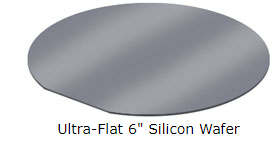
Ultra-Flat 6" Silicon Wafers 6 Ultra-Flat "Silicon Wafer with a large diameter for demanding substrate research. A 6" wafer carrier is used to transport the 6" ultra-flat silicon wafer. Also available in Gel-Pak® cartons as 5 x 5mm, 5 x 7mm, and 10 x 10mm stealth-diced dies. Stealth dicing eliminates saw dicing's edge-chipping and cutting detritus, resulting in the cleanest, most uniform output conceivable. All of our products are packed in a class 10 clean environment. 6's characteristics "Ultra-Flat Wafer (150mm):
|
|
Ultra-Flat Thermal SiO2 Substrates
A 200nm thermally generated amorphous SiO2 coating atop an ultra-flat silicon wafer makes up the Ultra-Flat SiO2 substrates. SiO2 is a well-studied substance that is widely utilised in semiconductor manufacturing, thin film research, and as a cell growth substrate. It can be used as an image substrate for AFM and SEM. Thermal silicon dioxide substrates with ultra-flat surfaces are available in 6" wafers and diced 5 x 5mm, 5 x 7mm, and 10 x 10mm chips. The diced parts are sent in a Gel-Pak® package, while the 6" wafer is sent in a 6" wafer carrier.
The clean dicing technique comprises coating the wafer with photo resist before dicing and removing it afterward, resulting in debris-free SiO2 substrates. All of our products are packed in a class 10 clean environment.
Properties for thermal SiO2 substrates:
- Grade: Prime Material: CZ Virgin Silicon Wafer Diameter: 150mm
- Orientation: Orientation: Orientation: Orientation: Orientation: Orientation: Orientation
- P/Boron is the type/dopant.
- 10-20 Ohm-cm resistivity
- 675 +/- 25m in thickness
- TTV: 2m TTV: 2m TTV: 2m TTV: 2m TTV: 2m TTV
- Flatness of the site: 1 m
- 30 m/sec warp
- 20 metre bow
- Particles: 20 at 0.2m
- Polished front surface
- Etched on the back surface
- 1 per SEMI Standard, flat
- Thermal Oxide Concentration: 2000A +/- 5%

|
- 3mm Discs with Silicon Nitride Coating (blanks)
- These 3mm silicon discs include a 50nm extremely low stress silicon nitride layer (Si3N4) on both sides that is ultra flat (RA of 0.450.02nm) and can be utilised for a variety of applications:
- Specimen mounts for use in SEM and FESEM.
- Specimen discs with a Si3N4 backdrop for AFM applications.
- Blanks for constructing the PELCO® Liquid CellTM, as well as PELCO® Silicon Nitride Membrane
Specifications include:
- 50nm very low stress Si3N4 film thickness on each sides
- 200m silicon support disc thickness
- The diameter of the disc is 3mm.
- Roughness of the surface: The RMS (Rq) is 0.65 +/- 0.06nm, resulting in a mean roughness (Ra) of 0.45 +/- 0.02nm.
- Merchandising PELCO® Silicon Nitride Discs are packaged in a vial that holds 10 discs in a cleanroom environment.

|
Single Crystal Substrates (NaCl, KBr and KCl) High purity, optical grade single crystals of sodium chloride (NaCl) MSDS, potassium bromide (KBr) and potassium chloride (KCl) form excellent substrates to grow epitaxial films. Single crystal films are created when the orientation of the vacuum coated thin films is directly connected to the orientation of the single crystal substrate. Ideal for thin film research, education, and single crystal film property studies. Impurities make up less than 1% of the total. | |||||||||||||||||||||||||||
All three materials come in packs of five with (100) orientation and a crystal size of 10 x 10 x 10mm. Freshly cleaved substrates are recommended for most applications. The split surfaces generate atomically flat patches, but predict cleavage steps across various atomic planes. 
| |||||||||||||||||||||||||||
Quartz Glass Substrate Discs by PELCO® PELCO® Quartz Glass Discs or Wafers are machined and optical-grade clear polished on both sides from high quality fused quartz (glassy, amorphous material - not a single crystal) (Technical Data on GE 124 Quartz). The discs work well as thin film substrates and can also be used for optical research. The chemical resistance of these quartz wafers to a wide range of solvents is outstanding. They also offer strong dimensional stability and strong heat resistance over a wide temperature range. Transparency is available from 0.19 to 4.2 m, with very low absorption between 0.26 and 2.6 m. With 60/40 scratch/dig requirements, the surface flatness is 1 degree. Available in diameters ranging from 1" to 4" with thicknesses of 1/16" and 1/8". |
| |||||||||||||||||||||||||||||||||||||||||||||||||||||
PELCO® Sapphire Substrate Discs PELCO® Sapphire Discs or Wafers are formed of high purity transparent sapphire (Al2O3) that has been machined and polished optically clear on both sides. (Sapphire Technical Data). Sapphire has a broad transmission range of 150 to 6000nm, with low absorption between 300 and 4500nm. The discs are appropriate for optical research and are ideal as substrates for thin film research. Resistance to a wide range of chemicals is excellent. Each face should be polished to a microinch or better. Tolerances in diameter and thickness are 0.001" (0.025mm); flatness is 0.0003" (0.0008mm) or better. Available in diameters of 0.5" (12.7mm), 0.75" (19mm), and 1" (25.4mm), with a thickness of 0.010" or 0.125". (0.25 or 3.2mm). |

| PELCO Sapphire Substrate Discs PELCO® Sapphire Discs or Wafers are formed of high purity transparent sapphire (Al2O3) that has been machined and polished optically clear on both sides. (Sapphire Technical Data). Sapphire has a broad transmission range of 150 to 6000nm, with low absorption between 300 and 4500nm. The discs are appropriate for optical research and are ideal as substrates for thin film research. Resistance to a wide range of chemicals is excellent. Each face should be polished to a microinch or better. Tolerances in diameter and thickness are 0.001" (0.025mm); flatness is 0.0003" (0.0008mm) or better. Available in diameters of 0.5" (12.7mm), 0.75" (19mm), and 1" (25.4mm), with a thickness of 0.010" or 0.125". (0.25 or 3.2mm). Vacuum Evaporation Supplies for Wafer Carriers | |||||||||||||||||||||||||||||||||||||||||||||||||||||
| ||||||||||||||||||||||||||||||||||||||||||||||||||||||
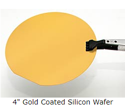
PELCO® Gold Coated Silicon Wafers 2" and 4" gold-coated silicon wafers for SEM or AFM supports, nanotechnology, and biotechnology. Both Cr and Au are evaporated on silicon wafers using a vacuum evaporation technique, with chromium serving as an adhesive layer between the glass and the gold. The gold surface is not atomically flat, but it does have nm-sized blemishes. A wafer carrier is used to pack and ship the wafers. At 175° C, the Au coating should be stable; above that temperature, delamination may occur. Wafer specifications:
PELCO® Gold Coated Microscope Slide Standard microscope slides made of high-quality glass with a 50nm gold coating and a 5nm chromium adhesion layer between the glass slide surface and the gold coating. It can be employed in a variety of nanotech, biotech, and AFM applications. Also works well as a microscope support that is opaque. A vacuum evaporation device is used to evaporate both Cr and Au on the glass slide. The gold surface is not atomically flat, but it does have nm-sized blemishes. In a slide mailer, the gold slides are separately packaged. The gold slides can be sterilised in an autoclave. Specifications include:

PELCO Gold Coated Glass Coverslips Standard microscope slides made of high-quality glass with a 50nm gold coating and a 5nm chromium adhesion layer between the glass slide surface and the gold coating. It can be employed in a variety of nanotech, biotech, and AFM applications. Also works well as a microscope support that is opaque. A vacuum evaporation device is used to evaporate both Cr and Au on the glass slide. The gold surface is not atomically flat, but it does have nm-sized blemishes. In a slide mailer, the gold slides are separately packaged. The gold slides can be sterilised in an autoclave. Specifications include:
| ||||||||||||||||||||||||||||||||||||||||||||||||||||||
1.3.7 Difference between Chip and Wafer in Electronics
A chip, also known as an integrated circuit, is a single-unit assembly of electronic components, whereas a wafer refers to thin slices of silicon that are utilised in the fabrication of integrated circuits since the integrated circuits are implanted in these wafers.
An integrated circuit, often known as a chip, is a compact electronic device that consists of a collection of circuits, paths, transistors, and other components that work together to perform a single task or a series of operations. Most modern electronic gadgets, such as microprocessors, audio and video equipment, and automobiles, rely on chips. The wafer contains the integrated circuit. Electronic components such as transistors are found on a chip. The term "microchip" is abbreviated to "chip." They're in charge of the logic circuitry.
A silicon wafer is used to make a chip. Chips come in a variety of shapes and sizes. Microprocessors are another name for CPU chips. Chips can be categorised into the following categories based on their electronic components:-
SSI (small-scale integration): each chip has up to 100 electronic components.
MSI (medium-scale integration): a chip with between 100 and 3,000 electrical components.
LSI (large-scale integration): a chip with between 3,000 and 100,000 electronic components.
VLSI (very large-scale integration): a chip with 100,000 to one million electronic components.
ULSI (ultra large-scale integration): a chip with over one million electronic components.
A wafer is also known as a slice or substrate in electronics. It's a sliver of cheese.
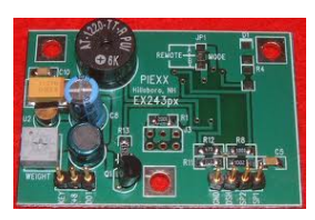
This slice is made of semiconductor material and is used to make integrated circuits. It serves as a foundation for the creation of an integrated circuit. These small slices are thought to be the brains of electronic devices. Diffusion and deposition of various chemicals are used to build microcircuits on wafers. In comparison to prior iterations, the ever-growing electronics industry always strives to create thinner chips that are more efficient and cost less.
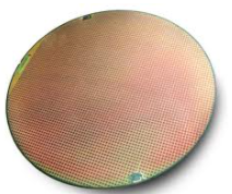
Through a series of procedures, raw silicon is transformed into a single crystal substrate. The majority of silicon is produced by reducing SiO2 with carbon, resulting in commercial brown metallurgical grade silicon. It also requires further purification, thus MG-Si is reacted with Hcl to produce TCS. Impurities such as Fe, Al, and B can be removed using this method. The samples with a solitary crystal orientation are then obtained by the crystal growth method. A spherical crystal is obtained afterwards with the help of monocrystalline seed. Wafers are thin slices of the crystal that have been cut into thin slices. After then, the growth process occurs, and lastly, various machines are used to achieve the desired qualities such as forms, etc. Wafers come in a variety of diameters.
The relationship between a wafer and a chip is what distinguishes them. A wafer serves as a foundation for a chip or is implanted in a wafer. They come together to produce an important unit that is frequently utilised in the electronics industry.
1.4.1 Hybrid Integrated Circuit
Individual components are bonded to a Ceramic substrate in a Hybrid Integrated Circuit. Metallization patterns or bonding wires are used to connect these components. On the chip, the active and passive components are dispersed. Hybrid ICs increase circuit performance by allowing passive components to be trimmed to precision at higher levels. This method is mostly utilised for low-volume customised circuits.
Classification of Hybrid Integrated Circuits
Hybrid Integrated Circuits (ICs) are classified into two variants based on the technology utilised to manufacture the passive components and related interconnections on the substrate: Thick Film and Thin Film ICs.
Film thickness on Thin Film ICs ranges from 50 to 20000 Armstrong units. Vacuum evaporation, plating method, sputtering, and screening are all techniques used to deposit thin films.
These ICs have a high component packing density as well as a high frequency packaging density. Resistors can be trimmed to precise values using this technology. Thin film ICs are suitable for ladder type Digital to Analog Converters because of this property.
The film thickness of Thick Film ICs ranges from 125000 to 625000 Armstrong units. This technology allows for the low-cost production of high-density circuits with passive components. Thick film deposition is accomplished using methods such as screen printing and substrate burning. These ICs are utilised in applications where high frequency and small size are crucial, such as vehicle electronic circuits, digital watches, and electronic toys.
Advantages
a. They are more compact and thus more portable.
b. They are more resistant to changes in physical characteristics.
c. The operating speed is high due to the lack of parasitic capacitance.
d. They have a low power consumption and can thus be powered by batteries.
e. The ICs are more reliable because there are no soldered joints.
f. A more straightforward design and standard packaging.
Disadvantages
The power dissipation of the ICs is poor due to their compact size. This, in turn, would destroy the IC due to the production of a large amount of heat owing to an increase in current.
1.4.2 Advantages and Disadvantages of Monolithic ICs
Monolithic IC
The term "monolithic" comes from the Greek words monos, which means "single," and lithos, which means "stone." As shown in fig. 1 (a), a monolithic circuit is created into a single stone or single crystal. In monolithic ICs, all circuit components (both active and passive) and their interconnections are created into or on top of a single chip or silicon (b).

Fig (a): Monolithic IC in Can-Type Enclosure
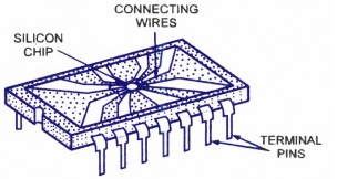
Fig (b): Monolithic IC in Plastic Package
Advantages of Monolithic ICs
1. The size is miniature. The IC is much smaller since the active and passive components are combined on a silicon chip utilising a fabrication process. It might be at least a thousand times smaller than a discrete circuit.
2. When compared to a discrete circuit, the IC's weight is reduced due to its tiny size.
3. The cost of manufacturing hundreds of ICs is relatively inexpensive, and it takes very little time. Producing hundreds of discrete circuits on a PCB for the same logic, on the other hand, takes longer and costs more.
4. The soldered joints on the PCB will be less reliable. Because there are no soldered joints and fewer interconnections in ICs, this problem is avoided, making them extremely dependable.
5. Because ICs are tiny, they consume less power and lose less power.
6. In discrete circuitry, a single defective transistor can cause the entire circuit to fail. This transistor requires desoldering and replacement. It's tough to figure out which part of the system has failed. Because replacing a complete IC is inexpensive, this problem can be avoided in an IC.
7. Higher operating speed due to the absence of parasitic capacitance.
8. Because the ICs are mass-produced, temperature coefficients and other properties will be very similar.
9. Improved functional performance due to the ability to fabricate more complicated circuits with better features.
10. All integrated circuits are evaluated for operating ranges in extremely cold and extremely hot temperatures.
11. Since all of the components in an IC are built very close to one another, they are ideal for small signal operation because there will be no stray electrical pickup.
12. There will be no exterior projections because all of the components are created inside the chip.
Monolithic integrated circuits have been used to perform a wide range of operations since their creation. Amplifiers, voltage regulators, crowbars, AM receivers, TV circuits, and computer circuits are all examples of commercially available ICs of this sort.
Disadvantages of Monolithic ICs
Monolithic circuits, on the other hand, have the following limitations or drawbacks:
1. The power rating is low. Since monolithic ICs are of about the size of a discrete small signal transistor, they typically have a maximum power rating of less than 1 watt. As a result, they can only be used in low-power applications.
2. There is a lack of isolation between the components.
3. There is no way to manufacture inductors.
4. The passive components utilised in the ICs have a limited range of values.
5. Circuit design lacks flexibility because each alteration in the circuit necessitates the use of a new set of masks.
1.5.1 Integrated Circuits (IC) – Concept, Classification
Integrated Circuits (IC’s)
In the year 1958, the notion of IC was initially introduced. Since then, this notion has advanced to greater technological heights than any other notion, allowing for the shrinking of a wide range of components in the digital world, including mobile phones, computers, laptops, and many more.
The invention of vacuum tubes ushered in the digital era. Vacuum-based computers were uncommon and costly. Transistors eventually took their place, as they were faster to use and smaller in size, as well as cheaper, less power-hungry, and more reliable. Then came the invention of integrated circuits, which completely changed how computers were used. Even the average person is familiar with its uses, such as smart phones and computers, because to its tiny size, low cost, and excellent durability.
Due to their excellent dependability and small size, the ICs have also found use in military applications, cutting-edge communication systems, and industrial applications. A modern integrated circuit (IC) the size of a fingernail contains over a million transistors and other discrete components. An integrated circuit, often known as a microchip, is a tiny chip constructed of a semiconductor material such as silicon that contains a collection of discrete circuits.
Due to two considerations, discrete circuits were phased out in favour of integrated circuits. The first is the use of space. Transistors, resistors, diodes, capacitors, and other discrete devices make up discrete circuitry. According to the circuitry requirements, each of them is soldered on to printed circuit boards (PCB). In the end, the PCB will take up a lot of room. Another disadvantage is that due to the large number of components used, the soldered components will be less reliable. Engineers were compelled to create microcircuits that were more reliable and took up less space as a result of both of these constraints.
In 1952, Geoffrey W. A. Dummer developed the concept of an integrated circuit for the first time. However, the endeavour to construct it was unsuccessful. Jack Kilby came up with another idea. He came up with the notion of making little ceramic wafers with a little discrete component on each one. After that, all of these wafers may be linked together to form a compact circuit. However, although being designed for the US army, this concept failed to gain traction and was abandoned.
Soon after, while working for Texas Instruments, the same Jack Kilby came up with the original idea for an IC. He began work on his first integrated circuit on September 12, 1958, and finished it on September 12, 1958. He used germanium as the semiconductor chip in his IC. In the year 2000, he was awarded the Nobel Prize in Physics for this discovery. Robert Noyce quickly created his own IC prototype using silicon as the semiconductor material. This invention assisted in the resolution of numerous practical issues with Jack Kilby's IC.
All integrated circuits (ICs) have both active and passive components, and the connections between them are so thin that even a microscope may not be able to see them. During the fabrication process, all of the components (active and passive) are connected.
There is no universal symbol for an integrated circuit in a circuit diagram. Dual in-line packages, metal cans, and ceramic flat packs are the most common options. Depending on the manufacturer's specifications, they may be 8-pin, 10-pin, or 14-pin connectors.
1.5.2 Integrated Circuit – Classification
All integrated circuits feature interconnected discrete devices on the inside and external connection terminals on the outside. Each pin may have a different function depending on the manufacturer's design. To make the circuit fully functional, the IC's pins must be used for supply voltage, input and output connections, as well as various external components depending on the manufacturer's requirements.
The following is a list of ICs that can be categorised based on their chip size:
- Small scale integration (SSI)—3 to 30 gates/chip.
- Medium scale integration (MSI)—30 to 300 gates/chip.
- Large scale integration (LSI)—300 to 3,000 gates/chip.
- Very large scale integration (VLSI)—more than 3,000 gates/chip.
1.5.3 SSI, MSI and LSI
Only a few transistors were used in the initial integrated circuits. A few logic gates were provided by early digital circuits with tens of transistors, while early linear ICs such as the Plessey SL201 or the Philips TAA320 had as little as two transistors. Since then, the number of transistors in an integrated circuit has skyrocketed. IBM scientist Rolf Landauer coined the word "large scale integration" (LSI) to describe the theoretical notion; it gave rise to the phrases "small-scale integration" (SSI), "medium-scale integration" (MSI), "very-large-scale integration" (VLSI), and "ultra-large-scale integration" (ULSI) (ULSI). SSI were the first integrated circuits.
Early aerospace projects required SSI circuits, and aerospace programmes aided in the development of the technology. The Minuteman missile and the Apollo programme both required lightweight digital computers for their inertial guidance systems; the Apollo guidance computer pioneered and encouraged integrated-circuit technology, while the Minuteman missile pushed it into mass manufacturing. In 1962, the complete $4 million integrated circuit market was accounted for by the Minuteman missile programme and numerous other Navy programmes, and by 1968, the U.S. Government expenditures on space and defence accounted for 37% of the $312 million overall production. The United States' demand The government backed the fledgling integrated circuit sector until costs dropped low enough for companies to break into the industrial and, subsequently, consumer industries. In 1968, the average price per integrated circuit fell from $50.00 to $2.33. By the turn of the decade, integrated circuits had made their way into consumer devices, with FM inter-carrier sound processing in television receivers being a common example.
Small-scale integrated chips for NASA spacecraft were the first MOS chips.
In the late 1960s, the next step in the development of integrated circuits was to introduce devices with hundreds of transistors on each chip, known as "medium-scale integration" (MSI).
Frank Wanlass exhibited a single-chip 16-bit shift register he designed in 1964, with an amazing 120 transistors on a single chip (for the time).
MSI devices were economically appealing because, though they cost slightly more to manufacture than SSI devices, they allowed for the production of more complicated systems with smaller circuit boards, less assembly effort (due to fewer individual components), and a variety of other benefits.
In the mid-1970s, due to the same economic pressures, "large-scale integration" (LSI) with tens of thousands of transistors per chip was developed.
SSI and MSI devices were frequently made with hand-cut Rubylith masks, which an engineer would inspect and check for completeness. Because LSI devices include so many transistors, interconnecting wires, and other characteristics, it is impractical for a human to examine the masks or even make the initial design by hand; the engineer relies on computer programmes and other hardware aids to handle the majority of the work.
Integrated circuits with less than 4000 transistors, such as 1K-bit RAMs, calculator chips, and the earliest microprocessors, began to be mass-produced in significant quantities in the early 1970s. Around 1974, true LSI circuits with over 10,000 transistors were first manufactured for computer main memories and second-generation microprocessors.
1.5.4 VLSI
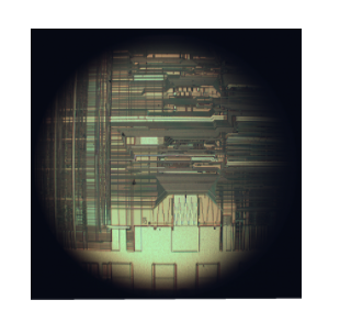
Upper interconnect layers on an Intel 80486DX2 microprocessor die
"Very-large-scale integration" was the final step in the development process, which began in the 1980s and continues now (VLSI). In the early 1980s, hundreds of thousands of transistors were developed, and by 2009, there were several billion transistors.
To accomplish this increased density, many developments were required. To build semiconductors with more transistors while maintaining appropriate yield, manufacturers shifted to smaller design guidelines and cleaner fabrication facilities. The International Technology Roadmap for Semiconductors described the direction of process advances (ITRS). Design technologies have advanced to the point that it is now feasible to complete these designs in a reasonable amount of time. NMOS and PMOS were replaced with the more energy-efficient CMOS, preventing a significant increase in power usage.
The first one-megabit RAM chips, with over one million transistors, were launched in 1986. In 1989, microprocessor chips surpassed the million-transistor milestone, and in 2005, they surpassed the billion-transistor milestone. The trend is still going strong, with devices having tens of billions of memory transistors being announced in 2007.
1.6.1 Digital ICs/Combinational Logic
What are Digital ICs?
The acronym IC stands for "integrated circuit," and it refers to any semiconductor-based chip that contains an integrated set of digital circuitry. Digital integrated circuits are available in a variety of shapes and sizes; the table below lists the IC types that are often utilised in diverse applications.
Microcomputers are integrated circuits (ICs) that do many sorts of processing.
Recollection
Data-storage integrated circuits
Logic ICs of the Standard Type
ICs assembled in various configurations to fulfil specific functions
Logic ICs Made to Order
Original dedicated circuitry created by or for a specific user's demands
A standard logic IC is a single, tiny integrated package that has basic components and common logic circuit functionality. These integrated circuits are essential parts of logic circuits. This type of IC will be the subject of today's presentation on digital ICs.
1.6.2 Standard Logic ICs: the Foundation of Digital Circuitry
From simple chips to fully functional arithmetic-and-logic units, there are around 600 different varieties of typical logic ICs. TTL and CMOS are two different forms of implementation.
TTL integrated circuits
Transistor-transistor logic integrated circuits (ICs): Bipolar transistors are used in the primary circuitry. These chips are powered by a 5-volt supply.
CMOS integrated circuits
Metal oxide semiconductor complementary integrated circuits: The primary circuitry is made up of pairs of p-type and n-type metal oxide semiconductor field-effect transistors (MOSFETs). The voltages utilised to power these chips span a wide range.
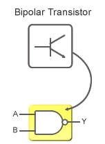
Figure: TTL IC
If a design requires signals to be transferred between digital ICs, the designer must understand the logical criteria that result in a H or L, as well as the voltage ranges that reflect these situations. Logic levels are voltage ranges that correspond to logical circumstances. Different logic levels used by communicating ICs will prohibit communication and may even cause IC failure.
TTL ICs utilise the following levels by convention.
Input Signals
0 V to 0.8 V is L; 2.0 V and up is H
Output signals
0 V to 0.4 V is L; 2.4 V and up is H
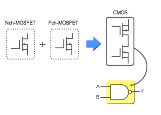
Figure: CMOS IC
TTL IC designers must adhere to the TTL interface specifications outlined above. Logic designers working with TTL IC communication no longer need to worry about logic levels because these values are now standard.
For CMOS ICs, the situation is different since there are many distinct series with varying logic levels, and the logic levels can also vary depending on the provided voltage. This means that when connecting multiple CMOS ICs, designers must use consistent logic levels.
1.6.3 The Significance of Fan-Out
When connecting ordinary logic ICs to a specific output, extreme caution must be exercised to avoid connecting too many ICs to a single output. The output current of TTL ICs restricts the number of IC connections. The greatest number of ICs that an output can connect to is referred to as fan-out.
Because TTL ICs are primarily made up of bipolar transistors, current is required to perform switching. The ratio of a TTL IC's output current to the current utilised by each input is known as fan-out (see Fig. 3). If fan-out is surpassed, there's a chance the output won't be able to keep up with the output logic levels.
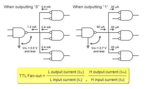
Figure: TTL IC Fan-out
Fan-out cannot be measured by looking at currents in CMOS ICs since very little current goes to the input terminals. Instead, load capacity determines fan-out. (Take a look at Fig. 4.) The propagation delay is used to determine the load capabilities listed on CMOS IC data sheets. If the load capacity is exceeded, the propagation delay may become so long that it causes a malfunction.
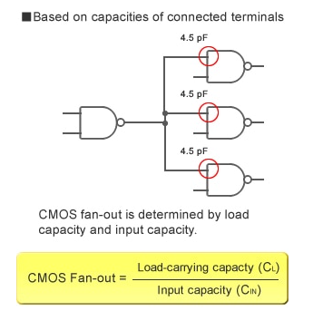
Figure: CMOS IC Fan-out
1.6.4 Open Drains: Wiring Outputs Together
Because there is no MOSFET on the VCC side of the output stage of a general-purpose CMOS IC in an open drain arrangement (Fig. A, left), the output cannot go High (Fig. A, right). Low or high-impedance output will be available (where the output pin is disconnected from the circuit and unable to output a voltage or current).
Because the output level is indeterminate, the high-impedance state is unstable. As a result, the output is connected to the power supply through an interposed pull-up resistor and set to High. It's worth noting that the voltage at which the output is connected to the pull-up resistor does not have to be the same as the power voltage. This enables the connection of ICs with different logic levels.

Figure: CMOS output and Open Drain output
1.6.5 combinational Logic
Combinational logic is a type of digital circuitry in which the output is solely determined by the current input signals. Sequential logic, on the other hand, is influenced not only by current inputs but also by internal memory and synchronous circuitry.
Let's have a look at combinational logic in today's lesson.
A combinational logic circuit is made up of multiple logic gates, such as AND, OR, NOT, XOR, and others. (Logic gates were discussed in a prior session.) A wide range of functions can be implemented with the right combination of logic gates. A multiplexer and a decoder are two common types of combinational logic.
1.6.6 Selecting Output Signals with a Multiplexer
A multiplexer is a signal switcher that chooses one output signal from several input signals. It works like a vending machine: you press one of the many accessible buttons, and the goods you choose appears at the machine's solitary outlet.
A multiplexer's action can be represented as a succession of switches, as seen in Fig.5. Both Switch A and Switch B have a bank of four internal switches each. As shown in the diagram, if Switch A and Switch B are both set to 0, input 0 will link to the output. In other words, the signal from input 0 will propagate through the output while the signals from the other inputs will be blocked. A = 1 and B = 0 picks output 1; A = 0 and B = 1 picks input 2; and A = 1 and B = 1 picks input 3. As you can see, the two switches A and B act as a multiplexer, allowing you to choose and propagate any of the four inputs.

Figure: Multiplexer: A Combination of Switches
Figure depicts a combinational logic representation of this multiplexer. The multiplexer can be created solely out of AND and OR gates, as you can see. The OR gate narrows down the AND section's decisions to just one.
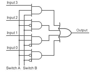
Figure: Multiplexer Implemented by Combinational Logic
1.6.7 Decoder: Decoding the Input
A decoder is a combinational logic circuit that, based on the logic of the inputs, switches one of multiple outputs ON (High). In terms of combinational logic, Figure depicts a decoder.
A truth table for this decoder is shown in Figure. The values of the two input signals pick one of the four potential output lines for actual output, as shown in the table. It's worth mentioning that we can call this circuit a decoder if we consider the input pair to be a binary value and the four output lines to be the decimal values 0, 1, 2, and 3.
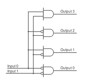
Figure: Decoder Implemented by Combinational Logic
Input1 | Input0 | Output3 | Output2 | Output1 | Output0 |
0 | 0 | 0 | 0 | 0 | 1 |
0 | 1 | 0 | 0 | 1 | 0 |
1 | 0 | 0 | 1 | 0 | 0 |
1 | 1 | 1 | 0 | 0 | 0 |
Figure: Truth Table of a Decoder
Combinational logic circuits can be utilised to make comparators, full adders, half adders, multipliers, subtracters, barrel shifters, and other functionality in addition to decoders. Only multiplexers and decoders of the type described above can be used to implement the majority of these functions. Even yet, circuits constructed only from these components are likely to have redundancy and other issues. As a result, these circuits must be simplified and compacted.
1.7.1 Binary number system
One of the four types of number systems is a binary number system. Binary numbers are represented by simply two symbols or digits in computer applications, namely 0 (zero) and 1 (one) (one). The base-2 numeral system is used to express the binary numbers. A binary number, for example, is (101)2. In this approach, each digit is referred to as a bit. Here's where you can learn about the number system.
In computer architecture, a number system is a means to represent numbers. There are four different kinds of number systems, for example:
1. The binary system of numbers (base 2)
2. System of octal numbers (base 8)
3. The decimal system (base 10)
4. The scheme of hexadecimal numbers (base 16).
In this article, let us discuss what is a binary number system, conversion from one system to other systems, table, positions, binary operations such as addition, subtraction, multiplication, and division, uses and solved examples in detail.
What is a Binary Number System?
A binary number is described as a number that is stated in the binary system or base 2 numeral system, according to digital technology and mathematics. It uses two distinct symbols to represent numerical values: 1 (one) and 0 (zero) (zero). The positional notation with 2 as a radix is known as the base-2 system.
Because of its direct application in electronic circuits utilising logic gates, the binary system is used internally by practically all modern computers and computer-based devices. A bit is a unit of measurement for each digit.
What is Bit in Binary Number?
The term "bit" refers to a single binary digit. A binary number is made up of several bits. Here are several examples:
A five-bit binary number is 1 10101.
A three-bit binary number is 2 101.
A six-bit binary number is 3 100001.
Binary Numbers Table
Some of the binary notations of lists of decimal numbers from 1 to 30, are mentioned in the below list.
Number | Binary Number | Number | Binary Number | Number | Binary Number |
1 | 1 | 11 | 1011 | 21 | 10101 |
2 | 10 | 12 | 1100 | 22 | 10110 |
3 | 11 | 13 | 1101 | 23 | 10111 |
4 | 100 | 14 | 1110 | 24 | 11000 |
5 | 101 | 15 | 1111 | 25 | 11001 |
6 | 110 | 16 | 10000 | 26 | 11010 |
7 | 111 | 17 | 10001 | 27 | 11011 |
8 | 1000 | 18 | 10010 | 28 | 11100 |
9 | 1001 | 19 | 10011 | 29 | 11101 |
10 | 1010 | 20 | 10100 | 30 | 11110 |
How to Calculate Binary Numbers
For example, the number to be operated is 1235.
Thousands | Hundreds | Tens | Ones |
1 | 2 | 3 | 5 |
This indicates,
1235 = 1 × 1000 + 2 × 100 + 3 × 10 + 5 × 1
Given,
1000 | = 103 = 10 × 10 × 10 |
100 | = 102 = 10 × 10 |
10 | = 101 = 10 |
1 | = 100 (any value to the exponent zero is one) |
The above table can be described as,
Thousands | Hundreds | Tens | Ones |
103 | 102 | 101 | 100 |
1 | 2 | 3 | 5 |
Hence,
1235 = 1 × 1000 + 2 × 100 + 3 × 10 + 5 × 1
= 1 × 10³ + 2 × 10² + 3 × 101 + 5 × 100
The decimal number system is based on the base 10 system, which uses the digits 0 through 9 to represent numbers. The digits 0-1 represent numbers in the binary system, which uses base 2, and the base is known as radix. To put it another way, the above table can also be displayed in the following way.
Thousands | Hundreds | Tens | Ones | |
Decimal | 103 | 102 | 101 | 100 |
Binary | 23 | 22 | 21 | 20 |
In base 10, we place the digits in columns 100, 101, and so forth. When a value greater than 9 is required, such as in the form of 10(n+1), you must first add 1 to column 101 before adding 10 to column 100.
In base 2, we position the digits in columns 20, 21, and so on. To place a value greater than 1 in 2n, multiply it by 2(n+1). To add 3 to column 20, for example, you must first add 1 to column 21.
Position in Binary Number System
We have ones, twos, fours, and so on in the Binary system...
For instance, 1011.110.
This is how it appears:
1 8 + 0 4 + 1 2 + 1 + 1 + 1 12 + 1 14 + 0 18
In decimal form, this equals 11.75.
The numbers can be placed to the left or right of the point to signify values higher than or less than one.
For 10.1, 10 is a whole number on the left side of the decimal, and the number place gets greater as we approach further left (Twice).
The first digit on the right is always 12 Halves, and the number grows smaller as we move further right (half as big).
In the above example:
In decimal, 1 “10” represents ‘2'.
2 The number “.1” denotes ‘half'.
3 As a result, "10.1" in binary equals 2.5 in decimal.
Binary Arithmetic Operations
We can conduct addition, subtraction, multiplication, and division operations on Binary numbers in the same way that we can conduct mathematical operations in numerals. Let's go over each one by one.
Binary Addition
When two binary integers are added together, we get a binary number. It is the most straightforward way. The table below shows how to add two single-digit binary numbers.
Binary Numbers | Addition | |
0 | 0 | 0 |
0 | 1 | 1 |
1 | 0 | 1 |
1 | 1 | 0; Carry →1 |
Let's have a look at adding two binary numbers as an example.
For example: Add 11012 and 10012.
Solution:

Binary Subtraction
We can get a binary number by subtracting two binary numbers. It's a simple procedure as well. The table below shows how to subtract two single-digit binary numbers.
Binary Numbers | Subtraction | |
0 | 0 | 0 |
0 | 1 | 1; Borrow 1 |
1 | 0 | 1 |
1 | 1 | 0 |
Let's have a look at subtracting two binary numbers as an example.
Example: Subtract 11012, and 10102.
Solution:

Binary Multiplication
The multiplication process for binary numbers is the same as it is for numerals. Let's have a look at an example.
Example: Multiply 11012 and 10102.
Solution:
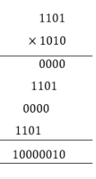
Binary Division
Binary division works in a similar way to decimal number division. Here's an example of what we're going to learn.
Example: Divide 10102 by 102
Solution:
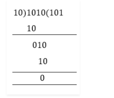
Uses of Binary Number System
In computer applications, binary numerals are frequently employed. All computer code and languages, such as c, c++, java, and so on. To construct a programme or encode any digital data, use the binary numbers 0 and 1. Only the coded language is understood by the computer. As a result, a two-digit number system is used to represent a collection of facts or information in discrete pieces of data.
1.7.2 Decimal to Binary Conversion Methods
The double dabbling approach is the most common way to convert a decimal integer to binary. The specified decimal number is divided by 2 in this way, with the remainder written after each division. The binary number is derived by reading all of the remainder in reverse order.
1.7.3 Steps for Decimal to Binary Conversion
Step 1: Divide the decimal number to be converted by two, which is the binary number's basis.
Step – 2 The least significant bit of the new binary number is the remainder produced in step 1.
Step – 3 Subtract the remainder from the quotient obtained in step 2, and the result is the binary number's second least significant bit.
4th step Rep the procedure till the quotient is 0.
5th step The most significant bit of the binary number is the last remnant received following division. As a result, order the numbers from most significant to least significant bits (i.e., from bottom to top).
This method can be simply understood if you consider the following example.
Take, for example, the translation of the decimal number 25 to its binary equivalent.
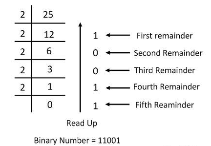
1.7.4 Conversion of Decimal to Binary for Fraction Number
Multiply by 2 and record the carry in the integral position for fractional decimal figures. When the carries are read down, the equivalent binary fraction is produced, as seen in the sample below.
Take the fractional binary integer 0.35 as an example.

Thus the fractional binary number is .01011, i.e., 0.01011.
The process of multiplication by 2 will continue till the desired accuracy is achieved.
1.7.5 Conversion of Decimal to Binary for Mixed Number
The same method is used to convert a decimal mixed number to a binary number as it used for integer and fractional components of the number. Consider the number 13.40 in decimal form.
The binary equivalents of 13 and 0.40 are 1101 and 011001, respectively. As a result, the needed binary number is 1101.011001.
1.7.6 Program for Binary to Decimal Conversion
We must create a software to convert a binary number into an equivalent decimal value given a binary value as input.
Examples:
Input: 111
Output: 7
Input: 1010
Output: 10
Input: 100001
Output: 33
The goal is to extract the digits of a binary number starting with the rightmost digit and store them in a variable called dec value. Multiply the digit with the suitable base (Power of 2) and add it to the variable dec value when extracting digits from the binary integer. Finally, the decimal number will be stored in the variable dec value.
Consider the following scenario:
111 is the binary number.
Dec_value = 1*(2^2) + 1*(2^1) + 1*(2^0) = 7
The graphic below shows how to convert ( 1010) to its decimal equivalent:
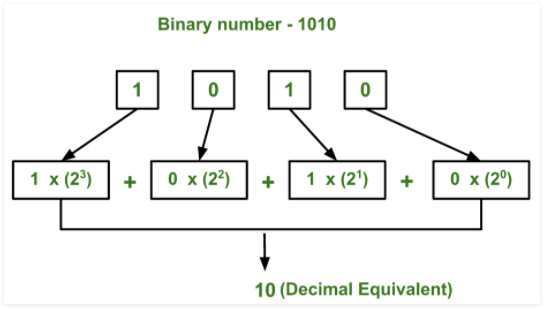
Below is the implementation of the above idea:
● C++
● Java
● Python3
● C#
● PHP
● Javascript
// C++ program to convert binary to decimal #include <iostream> Using namespace std;
// Function to convert binary to decimal Int binaryToDecimal(int n) { Int num = n; Int dec_value = 0;
// Initializing base value to 1, i.e 2^0 Int base = 1;
Int temp = num; While (temp) { Int last_digit = temp % 10; Temp = temp / 10;
Dec_value += last_digit * base;
Base = base * 2; }
Return dec_value; }
// Driver program to test above function Int main() { Int num = 10101001;
Cout << binaryToDecimal(num) << endl; } |
Output:
169
Note: The application can only work with binary numbers in the integer range. If you need to work with lengthy binary numbers, such as 20 bits or 30 bits, you can store them in a string variable.
Here's a similar programme that stores binary values in string variables rather than integers:
// C++ program to convert binary to decimal // when input is represented as binary string. #include <iostream> #include <string> Using namespace std;
// Function to convert binary to decimal Int binaryToDecimal(string n) { String num = n; Int dec_value = 0;
// Initializing base value to 1, i.e 2^0 Int base = 1;
Int len = num.length(); For (int i = len - 1; i >= 0; i--) { If (num[i] == '1') Dec_value += base; Base = base * 2; }
Return dec_value; }
// Driver program to test above function Int main() { String num = "10101001"; Cout << binaryToDecimal(num) << endl; } |
Output
169
#include <iostream> Using namespace std;
Int main() { Char binaryNumber[] = "1001";
Cout << stoi(binaryNumber, 0, 2);
Return 0; }
|
Output:
9
1.7.6 Binary to decimal formula
It's simple to convert a binary number to a decimal number or a decimal number to a binary number. However, you must be cautious not to confuse the two sets of numbers. For example, if you write the numerals 10 on a page, it may indicate the number “ten” if we believe it is a decimal number, or it may equally be a “1” and a “0” in binary, which is equal to the number two in the weighted decimal format from the table above.
Decimal Number=nthbit×2n−1
Binary to Decimal Formula:
N=bnqn+bn−1qn−2+…..+b2q2+b1q1+b0q0+b−1q−1+b−2q−2
Where,
N is decimal equivalent,
b is the digit,
q is the base value that starts from the most significant digit order qn to least significant order q-1, q-2, …..
To convert binary to decimal the following chart is used and binary is noted as per the given decimal number.
Binary | 0 | 1 | 10 | 11 | 100 | 101 | 110 | 111 | 1000 | 1001 | 1010 | 1011 | 1100 | 1101 | 1110 | 1111 |
Decimal | 0 | 1 | 2 | 3 | 4 | 5 | 6 | 7 | 8 | 9 | 10 | 11 | 12 | 13 | 14 | 15 |
If you use a binary number string, for example, you should include the subscript “2” to represent a base 2 number, making the binary number 102. Similarly, if it were a conventional decimal number, it would be expressed as 1010 with the subscript "10" to represent a base 10.

The process of converting binary to decimal is straightforward and can be done as follows:
Let's say we wish to convert the 8-bit value 10011101 to a decimal value. We can do it using the formula table below:
128 | 64 | 32 | 16 | 8 | 4 | 2 | 1 |
1 | 0 | 0 | 1 | 1 | 1 | 0 | 1 |
To convert, pick a value from the top row and place it where a 1 appears below it, then add the values together.
As a consequence, you will get 157.
1.8.1 BCD or Binary Coded Decimal
● Another method for converting decimal values to binary equivalents is Binary Coded Decimal, or BCD.
● It's a type of binary encoding in which each digit of a decimal integer is represented in bits.
● This encoding can be done in a 4-bit or an 8-bit format (usually 4-bit is preferred).
● In comparison to the existing binary system, it is a fast and efficient system for converting decimal numbers to binary values.
● These are commonly found in digital displays where data processing is a difficult operation.
● As a result of the manipulation, BCD plays a vital role because each digit is treated as a different single sub-circuit.
● In binary, many decimal values have an unlimited place-value representation, while in binary-coded decimal, they have a finite place-value. 0.2, for example, is.001100 in binary... And is 0.0010 in BCD. It is often utilised in large financial calculations to eliminate fractional errors.
● Take a look at the truth table below and think about how these are represented.
1.8.2 Truth Table for Binary Coded Decimal
DECIMAL NUMBER | BCD | ||
0 | 0000 | ||
1 | 0001 | ||
2 | 0010 | ||
3 | 0011 | 4 | 0100 |
5 | 0101 | 6 | 0110 |
7 | 0111 |
|
|
8 | 1000 |
|
|
9 | 1001 |
|
|
The specified decimal number is divided into chunks of four bits for each decimal digit inside the number in the BCD numbering system. Each decimal digit is translated to its binary equivalent (usually represented in 4-bits).
For example:
1. Convert (123)10 in BCD
From the truth table above,
1 -> 0001
2 -> 0010
3 -> 0011
Thus, BCD becomes -> 0001 0010 0011
2. Convert (324)10 in BCD
(324)10 -> 0011 0010 0100 (BCD)
Again from the truth table above,
3 -> 0011
2 -> 0010
4 -> 0100
Thus, BCD becomes -> 0001 0010 0011
This is how decimal numbers are converted to their equivalent BCDs.
It should be noted that the BCD is simply a binary representation of each digit of a decimal number; nevertheless, the BCD representation of the provided decimal number utilises extra bits, making it heavy-weighted.
1.8.3 Binary Coded Decimal
Another method for converting decimal values to binary equivalents is Binary Coded Decimal, or BCD.
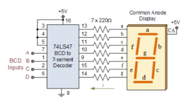
There are many different binary codes used in digital and electronic circuits, each with its own specialised function, as we've seen in this Binary Numbers part of lessons.
We need a mechanism to translate decimal numbers into a binary (base-2) environment that computers and digital electrical devices can understand because we live in a decimal (base-10) world. Binary coded decimal code allows us to do so.
An n-bit binary code is a set of “n” bits that can assume up to 2n different combinations of 1s and 0s, as we've seen before. The advantage of the Binary Coded Decimal system is that, like Hexadecimal, each decimal digit is represented by a group of four binary digits or bits. So we'll need a 4-bit binary code to represent the ten decimal digits (0–9).
Binary-coded decimal is not the same thing as hexadecimal. Binary coded decimal numerals stop at 9 binary 10012, although a 4-bit hexadecimal number is acceptable up to F16 meaning binary 11112 (decimal 15). Although 16 numbers (24) can be represented with four binary digits, the six binary code combinations 1010 (decimal 10), 1011 (decimal 11), 1100 (decimal 12), 1101 (decimal 13), 1110 (decimal 14), and 1111 (decimal 15) are classified as forbidden numbers in the BCD numbering system and cannot be used.
The fundamental benefit of binary-coded decimal is that it is simple to convert between decimal (base-10) and binary (base-2) forms. However, because the states between 1010 (decimal 10) and 1111 (decimal 15) are not used in BCD code, it is inefficient. Nonetheless, binary coded decimal has a wide range of uses, particularly in the context of digital displays.
A decimal number is divided into four bits in the BCD numbering system for each decimal digit inside the number. Each decimal digit is represented with a weighted binary value that translates the number directly. Each displayed decimal digit is represented by a 4-bit group, which ranges from 0000 for a zero to 1001 for a nine.
For example, the decimal number 35710 (three hundred and fifty-seven) would be represented in Binary Coded Decimal as:
0011 0101 0111 = 35710 (BCD)
The binary bit of each 4-bit group reflects a particular weight of the final result, indicating that BCD employs weighted codification. In other words, the BCD is a weighted code, with the weights 8, 4, 2, 1 (often referred to as the 8421 code) forming the 4-bit binary representation of the necessary decimal digit.
1.8.4 Binary Coded Decimal Representation of a Decimal Number

Each decimal digit to the left gains a factor of ten in decimal weight. Each digit's binary weight grows by a factor of two in the BCD number system, as indicated. Then the first digit has a weight of 1 ( 20 ), the second digit has a weight of 2 ( 21 ), the third a weight of 4 ( 22 ), the fourth a weight of 8 ( 23 ).
The following table shows the link between decimal (denary) numbers and weighted binary coded decimal digits.
Truth Table for Binary Coded Decimal
Decimal Number | BCD 8421 Code |
0 | 0000 0000 |
1 | 0000 0001 |
2 | 0000 0010 |
3 | 0000 0011 |
4 | 0000 0100 |
5 | 0000 0101 |
6 | 0000 0110 |
7 | 0000 0111 |
8 | 0000 1000 |
9 | 0000 1001 |
10 (1+0) | 0001 0000 |
11 (1+1) | 0001 0001 |
12 (1+2) | 0001 0010 |
… | … |
20 (2+0) | 0010 0000 |
21 (2+1) | 0010 0001 |
22 (2+2) | 0010 0010 |
The weights of each binary digit are then expressed as their four-bit pure binary counterpart, resulting in the 8421 BCD code.
1.8.5 Decimal-to-BCD Conversion
As we've seen, converting a decimal to a binary coded decimal is quite similar to converting a hexadecimal to a binary coded decimal. Separate the decimal number into its weighted digits first, and then write down the 4-bit 8421 BCD code for each decimal digit as indicated.
Binary Coded Decimal Example No1
Convert the decimal (denary) numbers 8510, 57210, and 857910 to their 8421 BCD equivalents using the table above.
57210 = 0101 0111 0010 = 8510 = 1000 0101 (BCD) (BCD)
1000 0101 0111 1001 = 857910 (BCD)
It's worth noting that the converted binary number is a real binary translation of decimal digits. Because the binary code is a real binary count, this is the case.
1.8.6 BCD-to-Decimal Conversion
The inverse of the above is the conversion from binary coded decimal to decimal. Simply divide the binary number into four-digit groups, starting with the least significant digit, and then write the decimal digit that each 4-bit group represents. If necessary, add more zeros at the end to make a complete 4-bit grouping. In decimal, 1101012 would be 0011 01012 or 3510, for example.
Binary Coded Decimal Example No2
Convert the following binary integers to decimal equivalents: 10012, 10102, 10001112, and 10100111000.1012.
This will create an error since the decimal 1010 is not a valid BCD number. 10012 = 1001BCD = 910 10102 =
10001112 = 0100 0111BCD = 4710; 10001112 = 0100 0111BCD = 4710; 10001112 = 01
0101 0011 0001.1010BCD = 538.62510 = 10100111000.1012 = 0101 0011 0001.1010BCD = 538.62510
Converting BCD to decimal or decimal to BCD is a simple operation, but it's important to understand that BCD numbers are decimal numbers, not binary numbers, despite the fact that they're expressed in bits. The BCD representation of a decimal number is crucial to grasp because most people's microprocessor-based systems employ the decimal system.
While BCD is simple to code and decode, it is inefficient for storing numbers. The number of individual data bits required to represent a specific decimal number in the standard 8421 BCD encoding of decimal numbers will always be more than the number of bits necessary for an equal binary encoding.
For example, a three-digit decimal number from 0-to-999 in binary requires just 10-bits (11111001112), however the same value in binary coded decimal requires a minimum of 12-bits (0011 1110 0111BCD).
Also, because each digit cannot exceed 9, executing arithmetic operations with binary coded decimal values can be a little problematic. In BCD, adding two decimal digits results in a possible carry bit of 1, which must be added to the next set of four bits.
The corresponding BCD digit is correct if the binary sum with the extra carry bit is equal to or less than 9 (1001). However, if the binary total exceeds 9, the result is an invalid BCD digit. As a result, it's preferable to convert BCD numbers to pure binary, add the appropriate numbers, and then convert back to BCD before showing the results.
Nonetheless, in both microelectronics and computer systems, the use of a BCD coding system is especially useful in situations where the binary coded decimal is intended to be displayed on one or more 7-segment LED or LCD displays, and there are many popular integrated circuits available that are configured to give a BCD output or outputs.
The 74LS90 asynchronous counter/divider, for example, features separate divide-by-2 and divide-by-5 counters that may be combined to create a divide-by-10 decade counter with BCD outputs. Another option is the 74LS390, which is a dual version of the 74LS90 that can also create a BCD output.
The 74LS47 and 74LS48 BCD to 7-segment decoder/drivers, which transform a 4-bit BCD code from a counter, etc. into the appropriate display code to drive the individual segments of a 7-segment LED display, are the most often used BCD encoded ICs. While both ICs perform the identical functions, the 74LS47 has active-low outputs for common-anode displays and the 74LS48 has active-high outputs for common-cathode displays.
1.8.7 Binary Coded Decimal Decoder IC

Binary Coded Decimal Summary
As we've seen, Binary Coded Decimal, or BCD, is essentially a 4-bit binary code representation of a decimal digit, with each decimal digit replaced with its binary equivalent in the integer and fractional sections. The ten decimal digits of 0 to 9 are represented by four bits in BCD Code.
For example, if we wanted to display decimal numbers from 0-to-9, we'd need 4 data bits (a nibble), decimal numbers from 0-to-99, we'd need 8 bits (one byte), decimal numbers from 0-to-999, we'd need 12 bits, and so on. Packed BCD is defined as the use of a single byte (8 bits) to store or display two BCD digits, allowing a byte to hold a BCD number in the range of 00 – 99.
A weighted 8421 BCD code is a standard binary coded decimal code in which the weights of the individual bits are represented by 8, 4, 2, and 1, starting with the most significant bit (MSB) and progressing to the least significant bit (LSB) (LSB). The individual places of the bits in a BCD code are weighted as follows: 23 = 8, 22 = 4, 21 = 2, 20 = 1.
The fundamental advantage of the Binary Coded Decimal system over the pure binary system is that it is a faster and more efficient approach for converting decimal numbers to binary values. However, the BCD code is inefficient since many of the 4-bit stages (10-to-16) are not used, whereas decimal displays are useful.
1.9.1 hexadecimal number system
Base 16 is used to represent numbers in the hexadecimal number system. It can alternatively be pronounced as 'hex'. Hexadecimal conversion is feasible, just as binary, octal, and decimal numbers, which have base representations of 2, 8, and 10, respectively. This subject is well-explained in the ninth-grade curriculum. The table below contains a list of 16 hexadecimal digits and their decimal, octal, and binary representations, which will aid in number system conversion. This list can also serve as a translator.
Hexadecimal Numbers List
Decimal Numbers | 4-bit Binary Number | Hexadecimal Number |
0 | 0000 | 0 |
1 | 0001 | 1 |
2 | 0010 | 2 |
3 | 0011 | 3 |
4 | 0100 | 4 |
5 | 0101 | 5 |
6 | 0110 | 6 |
7 | 0111 | 7 |
8 | 1000 | 8 |
9 | 1001 | 9 |
10 | 1010 | A |
11 | 1011 | B |
12 | 1100 | C |
13 | 1101 | D |
14 | 1110 | E |
15 | 1111 | F |
Hexadecimal Number System Conversions
As we know, there are 16 digits in hexadecimal numbers, represented from 0 to 9 same like decimals, but after that, it starts with an alphabetical representation of preceding numbers such as A, B, C, D and E. Let's look at how to convert 'hex' to other number systems.
Hexadecimal to Decimal Number System Conversion
Here, you will see the representation of a hexadecimal number into decimal form.
Hexadecimal | 0 | 1 | 2 | 3 | 4 | 5 | 6 | 7 | 8 | 9 | A | B | C | D | E | F |
Decimal | 0 | 1 | 2 | 3 | 4 | 5 | 6 | 7 | 8 | 9 | 10 | 11 | 12 | 13 | 14 | 15 |
Decimal to Hexadecimal Number System Conversion
You now know how to convert a hexadecimal integer to a decimal. Let's look at how to convert a decimal integer to hexadecimal now. Follow the instructions below:
● Divide the number by 16 first.
● Divide the quotient by 16 once more.
● The hex value will be generated from the remainder.
● Repeat the procedures until the quotient is equal to zero.
Example: Convert (242)10 into hexadecimal.
Solution: Divide 242 by 16 and repeat the steps, till the quotient is left as 0.
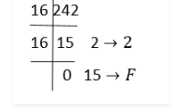
Therefore, (242)10 = (F2)16
Hexadecimal to Octal Number System Conversion
Here, you will see the representation of a hexadecimal number into octal number form.
Hexadecimal | 0 | 1 | 2 | 3 | 4 | 5 | 6 | 7 | 8 | 9 | A | B | C | D | E | F |
Octal | 0 | 1 | 2 | 3 | 4 | 5 | 6 | 7 | 10 | 11 | 12 | 13 | 14 | 15 | 16 | 17 |
Octal to Hexadecimal Number System Conversion
To convert an octal number to hexadecimal, first convert it to decimal, then decimal to hexadecimal. Let's look at an example to help us comprehend;
Consider the following scenario: Hexadecimal representation of (121)8.
To begin, convert 121 to a decimal number.
1 82 + 2 81 + 1 80 = 1 82 + 2 81 + 1 80
1 x 64 + 2 x 8 + 1 x 1 x 1 x 1 x 1 x 1 x 1 x 1 x 1 x 1
64 + 16 + 1 =
81 words
(8110) + (121)8
Now we're going to convert 8110 to hexadecimal.
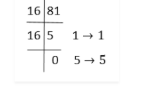
Therefore, 8110 = 5116
Hexadecimal to Binary Number System Conversion
The encoding of a hexadecimal number in binary form is shown here. Each hexadecimal number can be represented with only four digits, with each group having a different value ranging from 0000 (for 0) to 1111 (for F= 15 =8 + 4 + 2 + 1).
Hexadecimal | 0 | 1 | 2 | 3 | 4 | 5 | 6 | 7 | 8 | 9 | A | B | C | D | E | F |
Binary | 0 | 1 | 10 | 11 | 100 | 101 | 110 | 111 | 1000 | 1001 | 1010 | 1011 | 1100 | 1101 | 1110 | 1111 |
Binary to Hexadecimal Number System Conversion
Converting from binary to hexadecimal is a simple process. All you have to do now is convert the binary numbers to hexadecimal numbers.
Example: Convert (11100011)2 to hexadecimal.
Solution: From the table, we can write, 11100011 as E3.
Therefore, (11100011)2 = (E3)16
1.9.2 Octal Number System
Another form of computer and digital numbering system that employs the Base-8 standard is the Octal Number System.
The Octal Numbering System is identical to the previous hexadecimal numbering system in theory, except that a binary number is broken into groups of only three bits in Octal, with each group or set of bits having a different value between 000 (0) to 111 ( 4+2+1 = 7 ).
As a result, octal numbers have only "8" digits (0, 1, 2, 3, 4, 5, 6, 7) and are thus a Base-8 numbering system, with q equal to "8."
The basic characteristics of an Octal Numbering System are that there are only eight unique counting digits from 0 to 7, each with a weight or value of only eight starting with the least important bit (LSB). Because it worked in counts of eight, inputs and outputs were in counts of eight, a byte at a time, octal numbers and the octal numbering system were particularly popular in the early days of computers for counting inputs and outputs.
The subscript 8 is used to identify a number represented in octal since the basis of an Octal Numbers system is 8 (base-8), which also denotes the number of distinct numbers employed in the system. An octal number, for example, is written as 2378.
The "octal number system," like the hexadecimal system, allows huge binary numbers to be converted into more compact and smaller groups. However, the octal numbering system is no longer as popular as the hexadecimal numbering system, and it has all but vanished as a digital base number system.
Representation of an Octal Number
MSB | Octal Number | LSB | ||||||
88 | 87 | 86 | 85 | 84 | 83 | 82 | 81 | 80 |
16M | 2M | 262k | 32k | 4k | 512 | 64 | 8 | 1 |
There are no numbers or letters used above 8, because the octal number system employs only eight digits (0 through 7), although the conversion from decimal to octal and binary to octal follows the same pattern as hexadecimal.
In octal, we need to add another column and start counting again, identical to how we do in hexadecimal.
1, 2, 3, 4, 5, 6, 7, 10, 11, 12, 13, 14, 15, 16, 17, 20, 21, and so on.
Again, don't be confused: 10 and 20 are 1 + 0 and 2 + 0 in octal, respectively, just as they are in hexadecimal. The following table shows the link between binary and octal numbers.
Octal Numbers
Decimal Number | 3-bit Binary Number | Octal Number |
0 | 000 | 0 |
1 | 001 | 1 |
2 | 010 | 2 |
3 | 011 | 3 |
4 | 100 | 4 |
5 | 101 | 5 |
6 | 110 | 6 |
7 | 111 | 7 |
8 | 001 000 | 10 (1+0) |
9 | 001 001 | 11 (1+1) |
Continuing upwards in groups of three | ||
Then we can see that one octal number or digit is comparable to three bits, and that with two octal numbers, 778, we can count up to 63 in decimal, with three octal numbers, 7778, we can count up to 511 in decimal, and so on.
Octal Numbers Example No1
Convert this binary number to its octal equivalent using our previous binary number of 11010101110011112. (base-2 to base-8).
Binary Digit Value | 001101010111001111 |
Group the bits into three´s starting | 001 101 010 111 001 111 |
Octal Number form | 1 5 2 7 1 78 |
Thus, 0011010101110011112 in its Binary form is equivalent to 1527178 in Octal form or 54,735 in denary.
Octal Numbers Example No2
Convert the octal number 23228 to its decimal number equivalent, (base-8 to base-10).
Octal Digit Value | 23228 |
In polynomial form | = ( 2×83 ) + ( 3×82 ) + ( 2×81 ) + ( 2×80 ) |
Add the results | = ( 1024 ) + ( 192 ) + ( 16 ) + ( 2 ) |
Decimal number form equals: 123410 | |
Then, when you convert octal to decimal, you'll see that 23228 in octal form equals 123410 in decimal form.
While Octal is another sort of digital numbering system, it is less generally used these days due to its flexibility. Instead, the more often used Hexadecimal Numbering System is employed.
1.10.1 Realisation of an OR gate using diodes
1. When both A and B are earthed (that is, when both are connected to low input 0), neither diode conducts and no voltage occurs across R. As a result, the voltage at C is zero in relation to the earth. As a result, the output Y is zero (in levels).
2. The diode D2 conducts when A = 0 and B = 1 (i.e., when connected to the positive terminal), while D1 does not. Because D2 is perfect, there is no voltage drop across it, but there is a complete 5V voltage drop across R at C, +5V with respect to ground. As a result, Y is 1. (in level).
D1 conducts when A = 1 and B = 0, while D2 does not. The output Y is 1 for the same reason as before (in level).
4. When A = 1 and B = 1, both diodes conducts since the diodes are ideal and connected in parallel, the voltage drop across R cannot exceed 5V, with C at +5V with respect to earth. As a result, the output Y will be 1. (in level).
The truth table of OR gate
A | B | C |
0 | 0 | 0 |
0 | 1 | 1 |
1 | 0 | 1 |
1 | 1 | 1 |
1.10.2 The AND gate
1. Both diodes D1 and D2 become forward biassed and conduct when A = 0 and B = 0. There is no voltage drop between either diode because the diodes are perfect. As a result, a 5V potential difference occurs across R, with C at zero potential with regard to the earth. As a result, the output Y is zero (in level).
2. D1 conducts diode D2 does not when A = 0, B = 1. There is no voltage drop in D1 because it is perfect. As a result, a 5V voltage drop occurs across R, with D at +5V and C at zero with respect to earth. The result is zero (in levels).
3. Output is 0 when A = 1 and B = 0 for the same reason.
When A = 1, B = 1, none of the diodes will conduct, and no current will flow through R. With regard to the earth, the potential at C is identical to the potential at D, which is +5V. As a result, output Y is 1.
A | B | Y |
0 | 0 | 0 |
0 | 1 | 0 |
1 | 0 | 0 |
1 | 1 | 1 |
1.10.3 The NOT gate
I When A = 0, the transistor's base is also earthed. The base function of the emitter is no longer forward biassed, but the base-collector function is now reverse biassed. Because the emitter current is zero, the base current is also zero, resulting in a collector current of zero. As a result, the output Y is 1. (in level).
(ii) The emitter base function becomes forward biassed when A = 1. Emitter current, base current, and collector current will all be present. Rb and Rc values can be changed to allow huge amounts of Ic to flow. The potential difference across Rc caused by forward biassing of the emitter is just 5V, which is exactly the same as the potential difference across Rc caused by the battery in the collector circuit. As a result, the output is zero (in level).
When the A input is zero (grounded), the transistor realises the NOT gate, and the base is grounded.
We'll receive a lot of output since the voltage lowers across the collector and emitter.
In a common emitter arrangement, when A is supplied +5 voltage, the base current increases, which causes the collector current to increase. As a result, the voltage drop across Rc increases, but the voltage drop collects and the emitter is zero, resulting in a zero output.
Even if you give a lot of input, the output is zero.
1.10.4 Logic Gates Using Diodes and Transistors
The digital system's building blocks are logic gates. In this tutorial, we'll look at how to make basic digital gates using diodes and transistors.
OR Gate Using Diode
There are two or more inputs and only one output in an OR gate. If one or more inputs are HIGH, the OR gate's output is HIGH. Below is a circuit schematic for a two-input positive logic OR gate utilising diodes and a resistor:
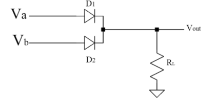
In this logic gate circuit, Va and Vb are inputs and Vout is output. These symbols can take only two values either LOW or HIGH.
Working:
Let's take a look at how this circuit works.
When all of the inputs are set to LOW, the diode is reverse biassed and behaves as an open switch. As a result, the output voltage is zero.
When A and B are both HIGH, the diode D1 becomes forward biassed and acts as a closed switch. As a result, the output is HIGH (ignoring diode forward resistance and voltage loss across the diode).
If A is low and B is high, then When diode D2 is forward biassed, it acts as an open switch. As a result, the output is extremely high.
If both inputs are HIGH, the output is equal to the input with the higher positive value.
As a result, the OR function has been added.
AND gate using diodes
There are two or more inputs and only one output in an AND gate. If all of the inputs are HIGH, the output of the logic AND gate is HIGH. The output is LOW for all other inputs.
The following is a circuit design for a two-input OR gate utilising diodes and a resistor:
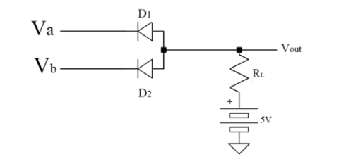
Here Va and Vb are inputs and Vout is output.
Working:
The diode D1 gets reversed biassed and acts as an open switch when A is HIGH and b is LOW. Furthermore, diode D2 becomes forward biassed and so acts as a closed switch. As a result, the output is LOW.
When A is LOW and B is HIGH, the diode D1 is forward biassed and hence acts as a closed switch. In addition, diode D2 is reversed biassed and so acts as an open switch. The output is VERY SMALL.
When all of the inputs are zero, the diode is forward biassed and acts as an open switch. As a result, the output is LOW.
When all of the inputs are HIGH, all of the diodes become reversed biassed and so behave as an open switch. As a result, the output is extremely high.
NOT gate using a transistor
NOT the gate Because the output is the polar opposite of the input, it is also known as an inverter. It has a single input and output. The following is a circuit diagram for a NOT gate that uses a transistor:
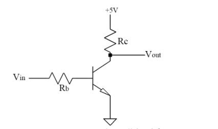
Vin is the input, and Vout is the output. If the input is HIGH, the output must be LOW. In addition, if the input is LOW, the output must be HIGH.
Working:
The parameter is chosen so that the output is V if the input is LOW (sat). In addition, if the input is HIGH, the parameter is chosen to produce a LOW output.
The transistor acts as an open switch when the input is LOW. As a result, the output is LOW.
The transistor acts as a closed switch when the input is HIGH. As a result, the output is VERY HIGH (Neglecting voltage drop).
1.11.1 Two Input Logic Gates
There are 16 logic gates for two logical inputs. Table 1 gives the logical symbol, behaviour in symbolic logic, name, and remarks for the 16 logic gates.
The ones with the names NAND, NOR, AND, OR, and XOR are the most well-known. These, as well as AND and OR gates with either input negated, logic 0 and logic 1 (which aren't truly logic gates), and certain non-binary gates, are all listed in Table.
| Output when AB is |
|
|
|
| |||
Gate # | 00 | 01 | 10 | 11 | Symbolic Logical Description | Symbol | Name/Description | Note |
0 | 0 | 0 | 0 | 0 | 0 |  | Always zero | Not really a gate |
1 | 0 | 0 | 0 | 1 | A & B |  | AND |
|
2 | 0 | 0 | 1 | 0 | A & ~B |  | A and Not B | Universal |
3 | 0 | 0 | 1 | 1 | A |  | A | Not BInary |
4 | 0 | 1 | 0 | 0 | ~A & B |  | B and Not A | Universal |
5 | 0 | 1 | 0 | 1 | B |  | B | Not Binary |
6 | 0 | 1 | 1 | 0 | (A & ~B) | (~A & B) |  | XOR | Also Not Equals Function |
7 | 0 | 1 | 1 | 1 | A | B |  | OR |
|
8 | 1 | 0 | 0 | 0 | ~(A | B) |  | NOR | Universal |
9 | 1 | 0 | 0 | 1 | (A & B) | (~A & ~B) |  | XNOR | Also Equals Function |
10 | 1 | 0 | 1 | 0 | ~B |  | Not B | Not Binary |
11 | 1 | 0 | 1 | 1 | A | ~B |  | A or Not B | Universal |
12 | 1 | 1 | 0 | 0 | ~A |  | Not A | Not Binary |
13 | 1 | 1 | 0 | 1 | ~A | B |  | B or Not A | Unversal |
14 | 1 | 1 | 1 | 0 | ~(A & B) |  | NAND | Universal |
15 | 1 | 1 | 1 | 1 | 1 |  | Always 1 | Not really a gate |
Table: 2 Input Logic Gates
1.11.2 NAND Gate is a Universal Gate
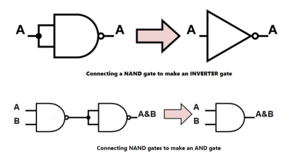
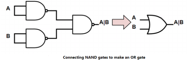
1.11.3 Other Universal Gates
The universal gates are 2,4,11, and 13. To exemplify this, we use these gates to create NAND gates. The gates 7 and 8 are the same gate with inverted inputs. The gates 9 and 10 are the same gate with inverted inputs. Proving the universality of gates 2 and 11 is sufficient to establish the universality of gates 4 and 13.
Gate 11: A | ~B
Gate 11 can be combined to produce INVERTER and AND gates, as seen in Figures. A NAND gate can be made by connecting INVERTER and AND gates in sequence. Gate 11 is a universal gate because it may be used to make a NAND gate, and a NAND gate is a universal gate. Gate 13 is a global gate since gates 11 and 13 are mirror images of each other.
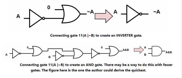
Gate 2: A & ~B
Gate 2 can be combined to produce INVERTER and AND gates, as seen in Figure below. A NAND gate can be made by connecting INVERTER and AND gates in sequence. Gate 2 is a universal gate because it may be used to make a NAND gate, and a NAND gate is a universal gate. Gate 4 is a universal gate since gates 2 and 4 are mirror images of each other.

Conclusion
This article has covered logic gates and universal gates, as well as demonstrating that the NAND gate is a universal gate and demonstrating the existence of four more universal logic gates. This is a fascinating academic activity. In practise, the author would advocate sticking to NAND gates as universal gates because they are so inexpensive and compact to build, or employing chips with the desired gates rather than universal gates if undertaking board level design.
1.11.4 Universal Logic Gates
With the NAND and NOR gates being minimal, Universal Logic gates can be utilised to construct any additional logic or Boolean function.
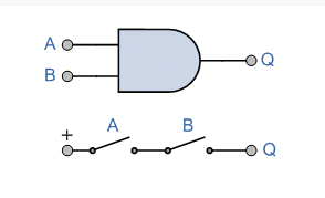
Individual logic gates can be linked together to create a wide range of switching functions and combinational logic circuits. The three most fundamental logic gates are the AND, OR, and NOT gates, as we've seen throughout this Digital Logic tutorial part, and with this set of logic gates, you can implement all of the conceivable Boolean switching functions, making them a "complete set" of Universal Logic Gates.
The numerous principles and theorems of Boolean Algebra can be realised with a complete set of logic gates by employing logical sets in this fashion. In fact, since the OR function can be built using only the AND and NOT gates, every other Boolean function can be built using only these two gates. Similarly, the AND function can be created by combining the OR and NOT functions.
A universal gate is any logic gate that can be joined into a set to realise all other logical functions, with a complete logic set being a collection of gates that can be utilised to build any other logic function.
For example, AND and NOT, as well as OR and NOT, provide a complete set of logic, as does cascading an AND with a NOT gate to form a NAND gate. In the same way, cascading an OR and NOT gate produces a NOR gate, and so on. The AND and OR functions, on their own, do not constitute a complete logic set.
We may design a variety of different Boolean functions and gates using these three Universal Logic Gates. The NAND and NOR gates, on the other hand, are classified as minimum sets since they have the feature of being a full set in and of itself, as they may be used alone or in combination to build a variety of other logic circuits.
Therefore we can define the complete sets of operations of the main logic gates as follows:
● AND, OR, and NOT are all terms that can be used to describe a condition (a Full Set)
● AND and NOT are terms that are used interchangeably (a Complete Set)
● OR and NOT are two terms that are used interchangeably (a Complete Set)
● NAND is a type of semiconductor (a Minimal Set)
● NORTH (a Minimal Set)
As a result, we may utilise these five sets of gates as building blocks to create more sophisticated logic circuits known as combinational logic circuits. But first, let's review the switching characteristics of the three most common logic gates: AND, OR, and NOT.
1.11.5 The AND Function
In mathematics, the product is the nu mber or quantity obtained by multiplying two (or more) numbers together. The AND function is the equivalent of multiplication in Boolean Algebra, hence its output state is the product of its inputs. Because the AND function is represented by a single “dot” (.) in Boolean Algebra, the Boolean equation for a two-input AND gate is Q = A.B, which means Q equals both A and B.
1.11.6 The OR Function
The sum in mathematics is the number or amount generated by multiplying two (or more) numbers together. The OR function is the equivalent of addition in Boolean Algebra, hence its output state represents the sum of its inputs. The OR function is represented by a "plus" symbol (+) in Boolean Algebra, hence the Boolean equation for a two-input OR gate is Q = A+B, which means Q equals either A OR B.
The 2-input Logic OR Gate
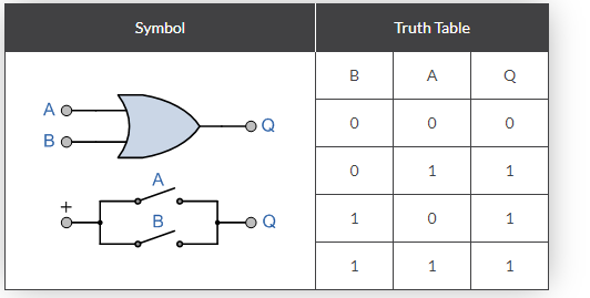
1.11.7 The NOT Function
The NOT gate, also known as a "inverter," has a sign that looks like a triangle pointing to the right with a circle at the end. An "inversion bubble" is the name given to this circle.
The NOT function is used to invert or complement a digital signal and is not a decision-making logic gate like the AND or OR gates. In other words, the condition of its output will always be the polar opposite of the state of its input.
As seen, the NOT gate symbol has a single input and output.
The Logic NOT Gate
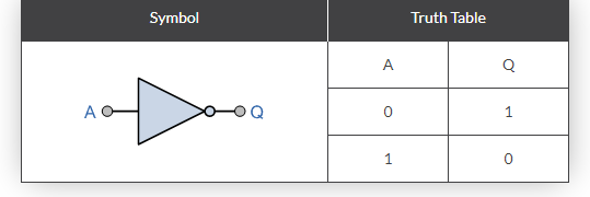
A digital buffer can be created by cascading the single input NOT gate or invert function with itself. The first NOT gate inverts the input, while the second returns it to its original level, resulting in a double inversion of the single input. Non-inverting Digital Buffers are useful in digital electronics because they can provide digital amplification and circuit isolation by doubly inverting the input.
1.11.8 Using the AND and NOT Set
Using just the AND and NOT set of logic gates we can create the following Boolean functions and equivalent gates.
AND/NOT Set Equivalents

1.11.9 Using the OR and NOT Set
Using the OR and NOT set of logic gates we can create the following Boolean functions and equivalent gates.
OR/NOT Set Equivalents
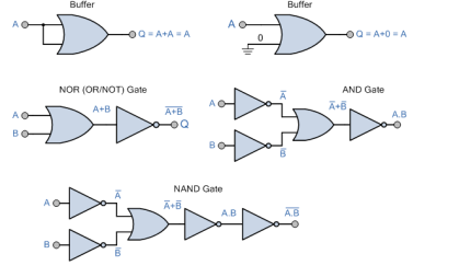
1.11.10 Using the Full AND, OR and NOT Set
We can generate the Boolean expressions for the Exclusive-OR (Ex-OR) and NOT Exclusive-OR (Ex-NOR) gates using the whole AND, OR, and NOT set of logic gates, as illustrated.
Full AND/OR/NOT Set to Implement Ex-OR
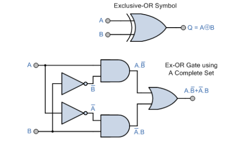
Full AND/OR/NOT Set to Implement Ex-NOR
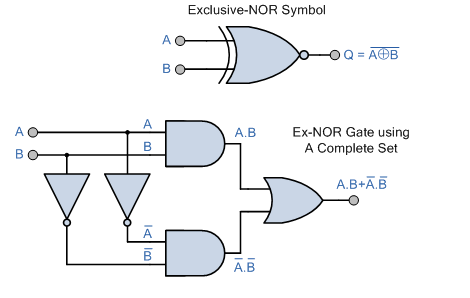
Note that neither the Exclusive-OR nor the Exclusive-NOR gates can be classified as universal logic gates because they cannot be utilised to construct any other Boolean function on their own or in combination.
1.11.11 Universal Logic Gates
One of the key disadvantages of employing the whole sets of AND, OR, and NOT gates is that we need two (or more) different types of logic gates, AND and NOT, OR and NOT, or all three as shown above, to generate any equivalent logic gate or function. All of the other Boolean functions and gates, on the other hand, may be implemented using just one form of universal logic gate, the NAND (NOT AND) or NOR (NOT OR) gate, minimising the number of various types of logic gates necessary as well as the cost.
The NAND and NOR gates are the complements of the previous AND and OR functions, respectively, and are each a full set of logic in and of themselves, as they can be used to build any other Boolean function or gate. However, because we may build further logic switching functions using just these gates, they are both referred to as a minimal set of gates. As a result, the NAND and NOR gates are known as Universal Logic Gates.
Implementation of Logic Functions Using Only NAND Gates
The quad 2-input NAND TTL chip 7400 (or 74LS00 or 74HC00) features four independent NAND gates in a single IC package. As a result, we can construct all of the Boolean functions from a NOT gate to a NOR gate using a single 7400 TTL chip, as shown.
Logic Gates using only NAND Gates
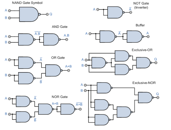
Thus ALL other logic gate functions can be created using only NAND gates making it a universal logic gate.
Implementation of Logic Functions Using Only NOR Gates
The quad 2-input NOR TTL chip 7402 (or 74LS02 or 74HC02) features four independent NOR gates in a single IC package. As with the preceding 7400 NAND IC, we can construct all of the Boolean functions from a single NOT gate to a NAND gate using a single 7402 TTL device, as shown.
Logic Gates using only NOR Gates
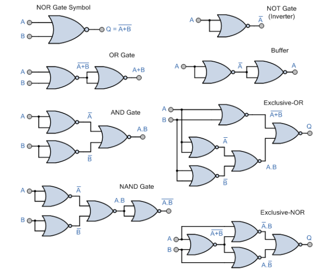
As a result, NOR gates can be used to produce any other logic gate function, making it a universal logic gate.
It's also worth noting that the Exclusive-OR gate is more efficient with NAND gates than with NOR gates, and the Exclusive-NOR gate is more efficient with NOR gates than with NAND gates because only four unique logic gates are required in each case. To put it another way, we can implement all of the Boolean functions with just one 7400 NAND or 7402 NOR chip, including all of its sub-families.
1.11.12 Universal Gate: NAND and NOR Gate as Universal Gates
What are Universal Gates?
A universal gate is a type of logic gate that can implement any Boolean function without the usage of any additional logic gates. The universal gates are the NOR and NAND gates. This means that using only NOR or NAND gates, you can build any logical Boolean statement.
In reality, this is beneficial because NOR and NAND gates are less expensive and easier to make than other logic gates. It's so common that an AND gate is implemented as a NAND gate followed by an inverter (rather than the other way around)! An OR gate, on the other hand, is usually implemented as a NOR gate followed by an inverter.
Other logical gates, such as AND gates, NOT gates, and OR gates, lack this universality trait. It's worth noting that these three logic gates can implement all of the conceivable Boolean switching functions when used together, but not when used separately. As a result, they are not classified as universal gates like the NOR and NAND logic gates.
Many of the better Arduino starter kits include these ubiquitous NOR and NAND gates if you want to experiment with them as part of an electronics project.
Now we'll take a look at how NOR and NAND gates work as universal gates.
NAND Gate As A Universal Gate
A two-input NAND gate is shown in the diagram below. The first portion is an AND gate, whereas the second portion is a NOT gate with a dot following it.
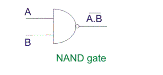
The inputs of the NAND gate are first passed through an AND gate, following which the output is inverted and the final output is obtained. Now we'll examine examine the NAND gate's truth table.
The truth table of the above NAND gate, which is a two-input NAND gate, will be considered. A and B are the two inputs.
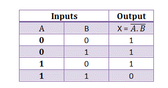
Now we will see how this gate can be used to make other gates.

This is the circuit diagram of a NAND gate that is utilised to make a NOT gate work; the original logic gate schematic of the NOT gate is also shown below.
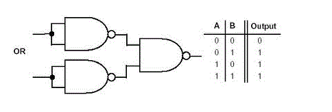
The above diagram is of an OR gate made from combinations of NAND gates, arranged in a proper manner. An OR gate's truth table is also shown next to the diagram.
Now we'll examine how to make an AND gate out of NAND gates.

An AND gate created from a NAND gate is shown in the diagram above. As we can see, all three basic gates may be created with simply NAND gates, which is why this gate is appropriately named Universal Gate.
NOR Gate As A Universal Gate
We've already shown how the NAND gate may be utilised to create all three fundamental gates by itself. Now we'll look at the NOR gate as an example.

An OR gate built entirely of NOR gates is shown in the diagram above. This gate produces an output that is identical to that of a single OR gate. The OR gate circuit, which uses NOR gates, is analogous to the AND gate circuit, which uses NAND gates.
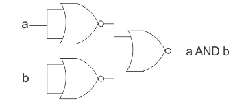
As the name implies, the above diagram is of an AND gate using only NOR gates. As can be seen, the circuit diagram of an AND gate using only NOR gates is identical to that of an OR gate using only NAND gates. We'll finally see what we can do now.
Make a NOT gate by using only NOR gates.

So, from the above discussion, it is clear that all the three basic gates (AND, OR, NOT) can be made by only using NOR gate. And thus, it can be aptly termed as Universal Gate.
1.12.1 The Exclusive-OR Gate
Only when both inputs are at opposite logic levels can the XOR gate produce a HIGH output.
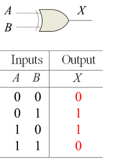
The XOR operation is written as  . Alternatively, it can be written with a circled plus sign between the variable as
1.12.2 Example waveforms for XOR:

Notice that the XOR gate will produce a HIGH only when exactly one input is HIGH.
1.12.3 The Exclusive-NOR Gate
Only when both inputs are at the same logic level can the XNOR gate create a HIGH output.
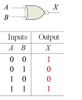
X= A B+AB is how the XNOR operation is written. It can also be expressed as X=AB with a circled dot sign between the variables.
Example waveforms for XNOR:

1.12.4 Parity Generator/Checker
The generation of parity, which is used to detect errors in transmitted data caused by noise or other disturbances, is one major application of the Exclusive-OR gate.
A parity bit is an additional bit added to a data word that can be either odd or even.
The total of all the bits (including the parity bit) in an even parity system is an even integer.
The sum of all the bits in an odd parity scheme must be an odd number.
The parity generator is the circuit that generates the parity bit at the transmitter.
The parity checker is a circuit that determines whether the data received is valid.
Only a single bit error can be detected using parity.
Exclusive-OR gates can be used to build both the parity generator and the parity checker.
To generate even parity, data bits are Exclusive-ORed together in groups of two until only one output remains. The parity bit is the result of this operation.
Simply flip the even parity to get odd parity.
An Exclusive-NOR gate can be used as the final gate.
To verify for parity, a new parity bit must be produced over the received date. This parity bit is then compared to the parity bit that was received. If they're the same, everything's ok. An Exclusive-OR gate can be used to perform the comparison.
The 74280 is a TTL IC that acts as a parity generator and checker.
XOR of two Binary Strings (1.12.2)
The aim is to print a string that is the XOR of Binary Strings A and B, given two binary strings A and B of equal length.
Examples:
Input: A = “0001”, B = “0010”
Output: 0011
Input: A = “1010”, B = “0101”
Output: 1111
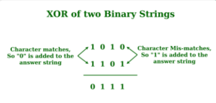
Below is the implementation of the above approach:
● C++
● Java
● Python3
● C#
● Javascript
// C++ Implementation to find the // XOR of the two Binary Strings #include<bits/stdc++.h> Using namespace std;
// Function to find the // XOR of the two Binary Strings String xoring(string a, string b, int n){ String ans = "";
// Loop to iterate over the // Binary Strings For (int i = 0; i < n; i++) { // If the Character matches If (a[i] == b[i]) Ans += "0"; Else Ans += "1"; } Return ans; }
// Driver Code Int main() { String a = "1010"; String b = "1101"; Int n = a.length(); String c = xoring(a, b, n); Cout << c << endl; } |
Output:
0111
References:
1. The Art of Electronics by Paul Horowitz and Wilfield Hill, Cambridge University -2006
2. Electronics by Allan R. Hambley, Prentice Hall - 1994
3. Digital Logic and Computer design M. Morris Mano (Pearson) -2016
4. Concepts of Electronics D.C.Tayal (Himalaya Publishing house) -2018


