UNIT 1
Electronics
- Signal
A signal is a description of how one parameter varies with another parameter.

For example: voltage changing over time in an electronic circuit.

Picture brightness : A camera senses the incoming light and records the light reflectivity as a function of space onto a magnetic film.
A Signal can also be called as a Wave. Every wave has a certain shape when it is represented in a graph. This shape can be of different types such as sinusoidal, square, triangular, etc. which vary with respect to time period or they may have some random shapes disregard of the time period.
Linear Wave Shaping
Linear elements such as resistors, capacitors and inductors are employed to shape a signal in this linear wave shaping. A Sine wave input has a sine wave output and hence the nonsinusoidal inputs are more prominently used to understand the linear wave shaping.
Filtering is the process of attenuating the unwanted signal or to reproduce the selected portions of the frequency components of a particular signal.
Filters
In the process of shaping a signal, if some portions of the signal are felt unwanted, they can be cut off using a Filter Circuit. A Filter is a circuit that can remove unwanted portions of a signal at its input. The process of reduction in the strength of the signal is also termed as Attenuation.
We have few components which help us in filtering techniques.
- A Capacitor has the property to allow AC and to block DC
- An Inductor has the property to allow DC but blocks AC.
Using these properties, these two components are especially used to block or allow AC or DC. The Filters can be designed depending upon these properties.
We have four main types of filters −
- Low pass filter
- High pass filter
- Band pass filter
- Band stop filter
Low Pass Filter
A Filter circuit which allows a set of frequencies that are below a specified value can be termed as a Low pass filter. This filter passes the lower frequencies. The circuit diagram of a low pass filter using RC and RL are as shown below.
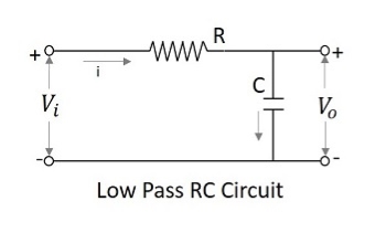
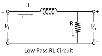
The capacitor filter or RC filter and the inductor filter or RL filter both act as low pass filters.
- The RC filter − As the capacitor is placed in shunt, the AC it allows is grounded. This by passes all the high frequency components while allows DC at the output.
- The RL filter − As the inductor is placed in series, the DC is allowed to the output. The inductor blocks AC which is not allowed at the output.
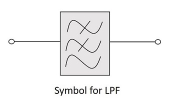
The symbol for a low pass filter LPFLPF is as given below.
Frequency Response
The frequency response of a practical filter is as shown here under and the frequency response of an ideal LPF when the practical considerations of electronic components are not considered will be as follows.

The cut off frequency for any filter is the critical frequency fcfc for which the filter is intended to attenuate cutcut the signal. An ideal filter has a perfect cut-off whereas a practical one has few limitations.
The RLC Filter
After knowing about the RC and RL filters, one may have an idea that it would be good to add these two circuits in order to have a better response. The following figure shows how the RLC circuit looks like.
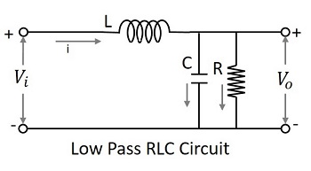
The signal at the input goes through the inductor which blocks AC and allows DC. Now, that output is again passed through the capacitor in shunt, which grounds the remaining AC component if any, present in the signal, allowing DC at the output. Thus we have a pure DC at the output. This is a better low pass circuit than both of them.
High Pass Filter
A Filter circuit which allows a set of frequencies that are above a specified value can be termed as a High pass filter. This filter passes the higher frequencies. The circuit diagram of a high pass filter using RC and RL are as shown below.
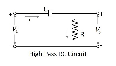
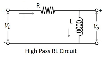
The capacitor filter or RC filter and the inductor filter or RL filter both act as high pass filters.
The RC Filter
As the capacitor is placed in series, it blocks the DC components and allows the AC components to the output. Hence the high frequency components appear at the output across the resistor.
The RL Filter
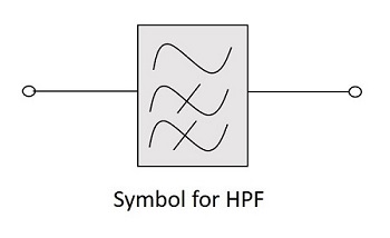
As the inductor is placed in shunt, the DC is allowed to be grounded. The remaining AC component, appears at the output. The symbol for a high pass filter HPFHPF is as given below.
Frequency Response
The frequency response of a practical filter is as shown here under and the frequency response of an ideal HPF when the practical considerations of electronic components are not considered will be as follows.

The cut-off frequency for any filter is the critical frequency fcfc for which the filter is intended to attenuate cutcut the signal. An ideal filter has a perfect cut-off whereas a practical one has few limitations.
The RLC Filter
After knowing about the RC and RL filters, one may have an idea that it would be good to add these two circuits in order to have a better response. The following figure shows how the RLC circuit looks like.
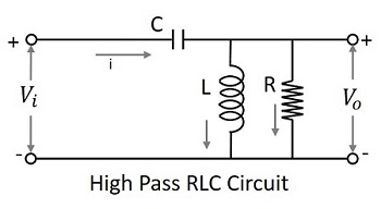
The signal at the input goes through the capacitor which blocks DC and allows AC. Now, that output is again passed through the inductor in shunt, which grounds the remaining DC component if any, present in the signal, allowing AC at the output. Thus we have a pure AC at the output. This is a better high pass circuit than both of them.
Band Pass Filter
A Filter circuit which allows a set of frequencies that are between two specified values can be termed as a Band pass filter. This filter passes a band of frequencies.
As we need to eliminate few of the low and high frequencies, to select a set of specified frequencies, we need to cascade a HPF and a LPF to get a BPF. This can be understood easily even by observing the frequency response curves.
The circuit diagram of a band pass filter is as shown below.
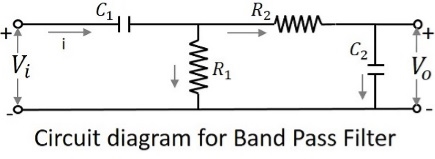
The above circuit can also be constructed using RL circuits or RLC circuits. The above one is a RC circuit chosen for simple understanding.
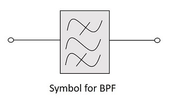
The symbol for a band pass filter BPFBPF is as given below.
Frequency Response
The frequency response of a practical filter is as shown here under and the frequency response of an ideal BPF when the practical considerations of electronic components are not considered will be as follows.

The cut-off frequency for any filter is the critical frequency fcfc for which the filter is intended to attenuate cutcut the signal. An ideal filter has a perfect cut-off whereas a practical one has few limitations.
Band Stop Filter
A Filter circuit which blocks or attenuates a set of frequencies that are between two specified values can be termed as a Band Stop filter. This filter rejects a band of frequencies and hence can also be called as Band Reject Filter.
As we need to eliminate few of the low and high frequencies, to select a set of specified frequencies, we need to cascade a LPF and a HPF to get a BSF. This can be understood easily even by observing the frequency response curves.
The circuit diagram of a band stop filter is as shown below.
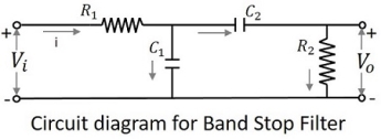
The above circuit can also be constructed using RL circuits or RLC circuits. The above one is a RC circuit chosen for simple understanding.
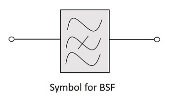
The symbol for a band stop filter BSFBSF is as given below.
Frequency Response
The frequency response of a practical filter is as shown here under and the frequency response of an ideal BSF when the practical considerations of electronic components are not considered will be as follows.

The cut-off frequency for any filter is the critical frequency fcfc for which the filter is intended to attenuate cutcut the signal. An ideal filter has a perfect cut-off whereas a practical one has few limitations.
Semiconductors are the materials which have a conductivity between conductors (generally metals) and non-conductors or insulators (such ceramics). Semiconductors can be compounds such as gallium arsenide or pure elements, such as germanium or silicon. Physics explains the theories, properties and mathematical approach governing semiconductors.
Examples of Semiconductors:
Gallium arsenide, germanium, and silicon are some of the most commonly used semiconductors. Silicon is used in electronic circuit fabrication and gallium arsenide is used in solar cells, laser diodes , etc.
In a p-type semiconductor, there is an increase in the density of unfilled states. Thus, accommodating more electrons at the lower energy levels. However, in an n-type semiconductor, the density of states increases, therefore, accommodating more electrons at higher energy levels.
Properties of Semiconductors
Semiconductors can conduct electricity under preferable conditions or circumstances. This unique property makes it an excellent material to conduct electricity in a controlled manner as required.
Unlike conductors, the charge carriers in semiconductors arise only because of external energy (thermal agitation). It causes a certain number of valence electrons to cross the energy gap and jump into the conduction band, leaving an equal amount of unoccupied energy states, i.e. holes. Conduction due to electrons and holes are equally important.
- Resistivity: 10-5 to 106 Ωm
- Conductivity: 105 to 10-6 mho/m
- Temperature coefficient of resistance: Negative
- Current Flow: Due to electrons and holes
N type Semiconductor:-
To increase the number of conduction band electrons inintrisic silicon , pentavalent imparity atoms are added. These are atoms with five valence electrons such as
i) arsenic (as)
Ii) phosphors (p)
Iii) Bismuth (Bi)
Iii) Antimony ( sb)
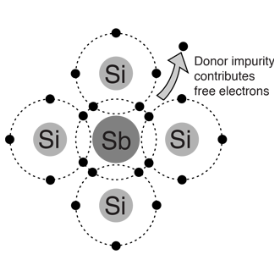
- Pentavalent impurity atom in a silicon crystal. An antimony (sb) impurity atom shown above-
- Each pentavalent atom forms covalent bonds with four adjustment silicon atoms, leaving one extra electron .
- The pentavalent atom gives up on electron , it often called a donor atom.
- Majority and minority carriers:- A type here means negative charge of an electron .electron are called the majority carriers in n-type material.
- Hole in an n-type material are called minority carriers
P Type Semiconductor :-
To increase the number of holes in intrinsic silicon trivalent impurity atoms are added these are atoms with their valence electrons such as
i) Baron(B)
Ii) Indium(IN)
Iii)Gallium(GO)
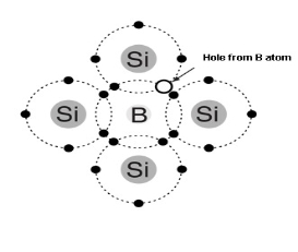
- Trivalent impurity atom in a silicon crystal structure . A) boron (B) impurity atom is shown in the center.
- The number of holes can be carefully controlled by the number of trivalent impurity atoms added to the silicon .
- A Hole created by the doping process is not accompanied by a conduction (free) electron.
- Trivalent Atom can take an electron it is often referred to as on accepted atom
Junction Diode: Principle of Diodes
V Barrier
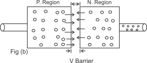
- A Forward biased showing the flow of majority carriers and the voltage due to the barrier potential across the depletion region-
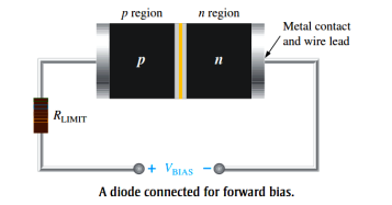
- To bias a diode apply d,c vtg across it .
- Forward bias is the condition that allows current through the PN junction.
- Negative side of VBIAS is connected to the N -region of the diode and the positive side is connected to the P- region.
- A selected requirement is that the bias voltage VBIAS must be greater than the barrier potential.
- Because of like charges repel, the negative side of the bias voltage source pushes the free electrons , which are the majority carriers in the N-region towards the PN junction .the flow of free is called Electron Current.
- The –Ve side of the source also provide a continues flow of electrons through the external connection (conductor).
- Into the N-region as show in fig-B
- The bias voltage source imparts sufficient energy to the free electrons for them to overcome the barrier potential of the depletion region and move on through into the 'p' region once in the P-region. These conduction electrons have lost enough energy to immediately combine with holes in the valence band.
- Now the e- are in the valance band in the P-region simply because they have lost too much energy overcoming the barrier potential to remain in the conduction band. Since unlike charge attract, the positive side of the bias voltage source attracts the valence electrons toward the left end of the region.
- The hole in the P-region provide the medium or "Pathway" for these valence electrons to move through the P-region.
- The holes which are the majority carriers in the P-region, effectively (not actually) move to the right toward the junction as shown in fig-B.
- The defective flow of holes is called the hole current.
- As from Fig-B hole current as the flow of valence electrons through the P-region with the holes providing the only means for these electrons to flow.
- As the electrons flow out of the P-region through the external connection and to the positive side of the bias in the P-region at the same time these electrons become conduction electrons in the mater conductor.
- To these is a continues availability of holes effectively moving towards the PN junction stream of electrons as they come across the junction in to the P-region.
The effect of forward bias on the depletion region:-

 + -
+ -


 -
-
Depletion Region
- Forward bias narrows the depletion region & produce a vtg drop across pn junction equal to the barrier potential.
- As more electrons flow into the depletion region , the number of positive ions is reduce . As more notes effectively flow into the depletion region on the other side of the pn junction ,the number of -ve ions is reduce this reduction in positive & -ve ions during forward bias causes the depletion region to narrow.
The Effect of the Barrier Potential during forward bias:-
- The electronic field between the positive and negative ions in the depletion region on either side of the junction creates an energy bill, that prevent free R form diffusing across the junction at equilibrium this is known as the barrier potential
- When forward bias is applied the free electrons are provided with enough energy from the bias voltage source to overcome the barrier potential and effectively climb the energy bill and cross the depletion region.
- The energy that the electronics repair in order to pass through the depletion region is equal to the barrier potential.
- Electron gives up an amount of energy equivalent to the barrier potential when they cross the depletion region.
- This energy loss results in a vtg drop across the pn junction equals to the barrier potential (0.7v)
- An additional small vtg drop across the P & N regions due to the internal resistance of the material.
- For doped Semiconductor material, this resistance called the dynamic resistance is very small and can usually be neglected.
REVERSE BIAS:-
Reverse bias is the condition the essentially prevents current through the diode.


P-region N- region


- +
V BIAS
A Diode connected for Reverse Biased-
- Because unlike charges attract the positive side of the bia voltage source pulls the free election, which are the majority carriers in the N-region away from the PN junction.
- AS the election flow towards the positive side of the voltage source additional positive ions are created
- This results in a widening of the depletion region and a depletion of majority carriers.


- The diode during the short transition time immediately after reverse bias vtg is applied-
- In the P-region electrons from the negative side of the vtg source enter as valence electron and move from hole to hole toward the depletion region where the creators additional -ve ions.
- This results in a widening of the depletion region and a depletion of majority carriers
- As the depletion region widens the availability of majority carriers decreases
- As more of the N & P regions become depleted of majority carriers, the electric field between the positive and -ve ions increase in strength the depletion region equals the bios vtg .this point the transition current essentially ceases except for a small reverse current that can usually be neglected.
Reverse Current
- Extremely small current that exist in reverse bias after the transition current dies act is caused by the minority carrier in the N& P region that are produced by the manly generated e hole pairs.
- The conduction band in the P-region is at a higher energy level then the conduction band in the N-region. Therefore, the minority easily pass through the depletion region because they required no additional energy.
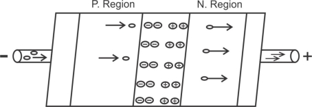
The Extremely small reverse current in a reverse biased diode is due to the minority carriers from thermally generated
e=hole pairs
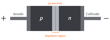
The Diode - Before doping the p-type & N-type consisting silicon material atom acting as a neutral.
IF a piece of intrinsic silicon is doped so that part is n-type and the other part is p-type, a junction forms at the bounded between the two regions and a diode is created.
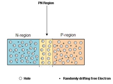
Formation of the Depletion Region
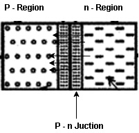
At the instant of junction formation , free electrons in the N-region near the p-n junction being to diffuse across the junction and fall into holes near the junction in the P-region.
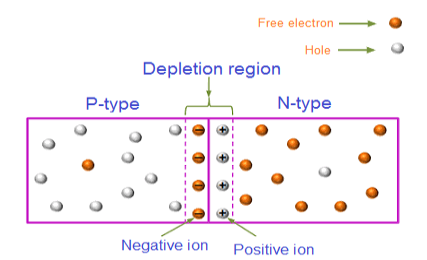
For every electron that defuse across the junction and combines with a hole , a positive charge is left in the region and a ve charge is created in the p-region firming a barriers potential. This action continues until the vtg of the barrier ripples further diffusion.
The Depletion region acts as a barriers to the farther movement of electrons across the junction
As positive ion & -ve ion across the junction produces a electric field across the junction -according to coulombs law.
The potential difference of the electric field across the depletion region is the amount of vtg required to move electronics through the electric field, this potential difference is called the barrier potential & is expressed in volt
The typical barrier potential is approximately 0.7 v for silicon & 0.3 v for germanium at 25c.
V-I characteristics of junction diode
A :- v=A Characteristic for forward bias:-
If (mA)


 C
C

 A B
A B
o 0.7V vf
V-I Characteristics:-
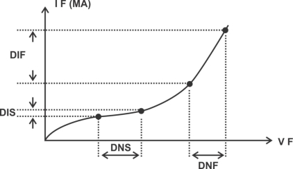
Graph shows how the dynamic resistance decrease as we move up the curve xd= DNF/DIF=
When the forward bias vtg is increased to a value where the vtg across the diode reaches approximately 0.7 v (barrier potential . The forward currant begins to increase rapidly
As we continue to increase the forward bias voltage the current continues to increase very rapidly ,but the voltage across the diode increase only gradually above 0.7 v.
This small increase in the diode vtg above the barrier potential is due to the voltage drop across the internal dynamic resistance of the semi conductive material.
Dynamic resistance:- A Resistance change as move along a V-I curve it is called dynamic or A. C resistance.
 |
B) V - I Characteristics for Reverse biased :-


 VR VBR 0
Knee
When the applied bias voltage is increased to a value where. The reverse vtg across the diode the reaches appropriately 0.7 v (barrier potential) the forward current begins to increase rapidly.
As we continue to increase the bias voltage the current continues to increase very rapidly bit the voltage across the diode increases very little above VBR.
IR increases little above VBR. Resulting in overheating & possible damage.
AC and DC Resistance of Diode
Static or DC Resistance
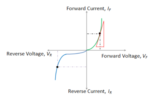
It is the resistance offered by the diode to the flow of DC through it when we apply a DC voltage to it. Mathematically the static resistance is expressed as the ratio of DC voltage applied across the diode terminals to the DC flowing through it (shown by the black dotted line in Figure) i.e.

Dynamic or AC Resistance
It is the resistance offered by the diode to the flow of AC through it when we connect it in a circuit which has an AC voltage source as an active circuit element. Mathematically the dynamic resistance is given as the ratio of change in voltage applied across the diode to the resulting change in the current flowing through it. This is shown by the slope-indicating red solid lines in Figure and is expressed as

Diode Current Equation
 ampers
Where ,
V= Applied voltage across the diode in volts
I=Current flow through the diode in amperes.
n= 2 for silicon P-N junction diode
=1 for germanium P-N junction diode.
IO = reverse saturation current flow through diode in amperes.
VT =Is the voltage equivalent of temperature in volts.
VT= K X T volt’s
K=Boltzmann's constant
K=8.62 * 10 -s ev/k
I= temperature in ok
The equation VI= K * T indicates that the current flow through the diode also depend upon the ambient temperature.
Room temperature =25 0c
T= 273+25=298K
VT=K * T


Equivalent circuit of Diode

Breakdown Mechanism
i) Avalanche breakdown:-As the magnitude of the reverse bias vtg is increased the kinetic energy of the minority carriers gets increased. While travelling the minority carriers collide with the stationery atoms which in turns results in breaking some of the covalent bond & generating free e- (carrier multiplication)
This process continues leading to a very swift multiplication giving rise to a large reverse current in just a few picoseconds. This effect is called as avalanche breakdown effect.
Topical Breakdown vtg is about 50v to 100v:-
i) Due to large power dissipation the junction temperature increase & may destroy the semiconductor device permanently.
Ii) Zener Breakdown: - This type of breakdown occurs in heavily doped P-N junction in which the depletion region is very narrow.
All the applied reverse voltage appears across the depletion layer. The electric field is vtg per unit distance. It is very intense at the depletion region.
There for it can pull the electronic out of the valance bond by breaking the covalent bonds and producing the free electrons. This process is known as zener effect.
Due to this heavy current flow & diode may damage.
Zener Diode
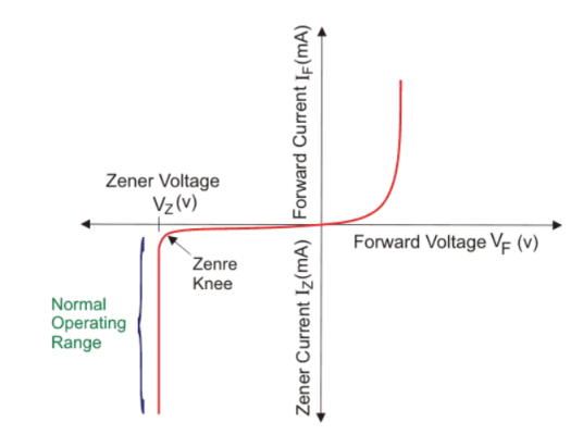
- Zener diode is a special type of p-n junction semiconductor diode in this diode the reverse breakdown voltage is adjusted precisely between 3v to 200v.
- Its applications are based on this principle hence Zener diode is called as a breakdown diode.
- The doping level of the imparity added to manufacture the zener diode is controlled in order to adjust the precise value of breakdown voltage.
PRINCIPLE OF OPERATION: - A zener diode can be forward biased or reverses biased. Its operation in the forward biased mode is same as that of a p-n junction diode but its operation in the reverse biased mode is sustainably deferent.

Numerical:
A 5.0V stabilized power supply is required to be produced from a 12V DC power supply input source. The maximum power rating PZ of the zener diode is 2W. Using the zener regulator circuit above calculate:
a). The maximum current flowing through the zener diode.
Maximum current = Watts/ Voltage =2W/5V =400mA
b). The minimum value of the series resistor, RS
 = 17.5 Ω
c). The load current IL if a load resistor of 1kΩ is connected across the zener diode.

d). The zener current IZ at full load.
Iz =Is -Il =440mA – 5mA = 395mA
Rectifier circuit
Half Wave rectifier
1) Due to the unidirectional current flow through the transformer there is a possibility of core saturation to avoid this transformer size must be increased.
2) Ripple factor is high.
3) Low rectification effecting.
4) Law TUF.
5) Law D.C O/P VTG & current.
6) Large filter component are required.
ADVANTAGES:-
1) Simple Construction.
2) Component required less.
3) Small size.
APPLICATION:-
Walkman, law cost power supply.
TRANSFORMER UTILISATION FACTOR (TUF):-It indicates how well the ilp transformer is being utilized
TUF= DC O/P Power / AC power rating of the transformer

Full Wave Rectifier
1) A centre tapped rectifier is a type of full wave rectifier that uses two diode connected to the secondary of a centre tapped transformer.
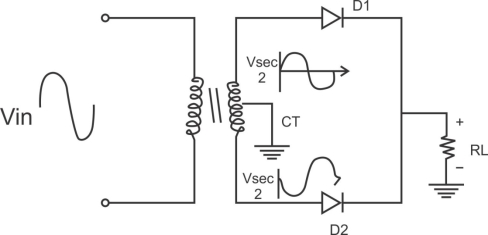
Center tapped full wave rectifier operation:-
I) During positive half cycle of i/p ac supply.
Diagram

D1.Is in forward biased & D2 is in reverse biased.
II)During -ve half cycle.

D1 Reverse biased
D2 Forward biased
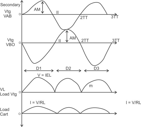
ADVANTAGES
1) law ripple factor as Compared to HKR.
2)Better rectification efficiency.
3) Better TUF.
4)Higher value of average load vtg & avg load crt.
5)No possibility of transformer core saturation.
DISADVANTAGES
PIV of diode is 2vm , more size costly.
APPLICATION
I) Battery charges.
2)power supply at laboratory, high current, electronic ckt.
Clipper and Clamper
Diode Clipper or Limiting Circuits :-
Diode C kts called limiters or clippers are sometimes used to clip off portions of signal voltages above or below certain levels.
Another type of diode ckt called a clamper is used to add or restore a d.c level to an electrical signal.
Below fig a) that limits or clips the positive part of the input voltage As the ilp vtg goes positive the diode become forward biased Because the cathode is at ground potential (ov)the anode cannot exceed 0.7v (for si)
So point A is limited to 0.7v the diode is reverse biased and appears as an open. The O/P VTG looks like the with a magnitude determined by the voltage divider formed by R1& the load resistor RL.
Vout=(RL/R1+RL) vin
If R1 small compared to RL then vout = vin

Clipper of the positive alternation. The diode is F,B during the +ve alternate RB during –ve alternation:-
Negative Clipper:-

Limiting of the negative alternation the diode is PB during the –ve alternation R.B during the +ve alternation.
During Reverse bias the +ve part of the ilp vtg is clipped off when the diode is forward biased during the –ve part of the ilp vtg is clipped off. When the diode is F.B during the –ve part of the ilp vtg point A is held at 0.7v by the diode is no longer forward biased and a voltage appears across RL proportional to the ilp vtg.
Problem:- What would you expect to see displayed on oscilloscope connected across RL in the Limiter.

The diode is forward biased and conducts when then the i/p vtg goes below -0.7v so for the –ve limiter , the peak o/p vtg across RL can be determined by the following
Equation -
Volt =(RL/R+RL) Vin
=(1k/100+1k)10v
= 1K/1.1K*10
=1*103/1.1*103*10
= 1*104/11*102*10
= 1*104*10-2*10
=10/11 10*10*10/11
Volt = 10000/11 = 9.09V
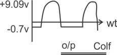
Biased parallel /Clipper :-1) The level to which an act voltage is limited can be adjusted by adding a bias vtg in series with the diode shown in fig.

The voltage at point A mast equal VBINS+0.7v before the diode will become forward biased & conduct
Once the diode begins to conduct the vtg at point A is limited to VBINS +0.7 so that all ilp above this level is clipped off

To limit a vtg to a specified –ve level the diode & bios vtg must be connected. In this case the vtg at point ‘A’ must go below –VBIN-0.7v to forward biased the diode & initiate limiting action
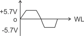
Prob:- fig shows a ckt combing a positive clipper with a-ve clipper .Determine the o/p vtg c/f

When the voltage at point A riches +5.7V diode A conducted and limits the waveform to +5.7v diode D2 does not conduct until the voltage reaches -5.7V
Therefore positive voltages above +5.7V & -ve voltages below -5.7V are clipped off
Diode Clampers:-
1) Positive Clamper:-
Diagram:-

Assumptions :-
1) The V/p is a perfect sine waveform
2)The value of R& C are chosen such that the Line constant T=RC is large equal
3)The diode is an ideal one
4)The Rc time constant is much longer as compared to one cattle period ‘T’ of the input.
RC >100T
Operation :-I n the first negative half cycle after turning on the Ckt the diode acts as a closed S/W & charges the capacitor to peak ilp vtg VM with the polarity shown below

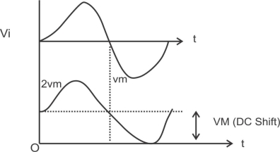
The diode reverse biased in both half cycle so it remains off.
2)Negative Clamper:-

In the first positive half cycle the capacitor will charge through the forward biased to peak vtg vm
The charging takes place very quickly as the diode resistances negligibly small
Once the capacitor charges to vm the diode is reverse biased and stops conducting.

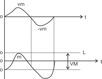
Diagram non ideal diode
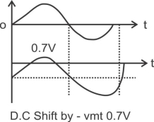
Biased Clamper:-
Diagram:-
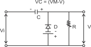
-Clamper with additional dc source:-
Diagram-
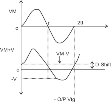
The load vtg W/F shows d.c level shift is positive but less than +vm
Level shift is given by
DG shift = vm - v
Operation:-
In the –ve half cycle ilp the diode will be forward biased and capacitor gets charged to a vtg (vm-v) volts with the polarities shown.
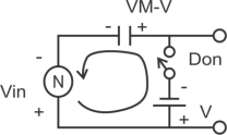
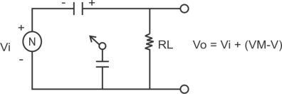
In above diagram during positive half cycle diode will remain permanently off therefore .the job of the diode is only to charge the capacitor.
Vo=vc +vi
Vo=(vm-v)+vi
Series clipper CKT:-
1)Series Negative clipper :- Ideal diode
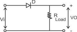
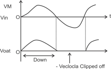
Operation:-
In the positive half cycle of the sinusoidal ilp the diode is forward biased. Being an ideal diode , it acts as a closed switch & connects the load across the ilp the load vtg there fore equal to the ilp vtg in the positive half cycle.
In the –ve half cycle of the diode is reverse biased acts as an open ckts/w the load vtg is therefore zero during the –ve half cycle.
2) Series Positive clipper:-

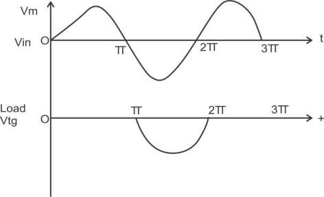
Series clipper with a D.C supply biased [clippers] :-
1) Biased Series – ve Clipper:-
2)


Operation:-
The operation of this ckt can be divided in to there intervals
1) Operation when in is +ve but less than v:-in the positive half cycle of the ilp as long as vin v the diode is not forward biased, therefore from to and then from t2 to t/2 shown in fig below the diode will remain in off state and the o/p voltage will be zero.

Fig -a) Equivalent ckt for +vin>v -
-
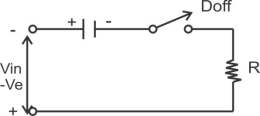
Fig b) Equivalent ckt for vin -ve
References:
- Basic Electrical Engineering” by C L Wadhwa.
- “ Basic Electrical Engineering” by Mehta V K and Mehta Rohit.
- “ Basic Electrical Engineering” by Nagrath, I and Kothari.