Interfacing is the method of connecting or linking together one device, especially a computer or micro-controller with another allowing us to design or adapt the output and input configurations of the two electronic devices so that they can work together.
But interfacing is more than just using the software program of computers and processors to control something. While computer interfacing uses the unidirectional and bidirectional input and output ports to drive various peripheral devices, many simple electronic circuits can be used to interface to the real world either using mechanical switches as inputs, or individual LEDs as outputs.
|
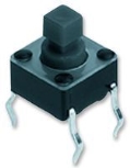
Fig 1 - Pushbutton Switch
For an electronic or micro-electronic circuit to be useful and effective, it has to interface with something. Input interface circuits connect electronic circuits such as op-amps, logic gates, etc. to the outside world expanding its capabilities.
Electronic circuits amplify, buffer or process signals from sensors or switches as input information or to control lamps, relays or actuators for output control. Either way, input interfacing circuits convert the voltage and current output of one circuit to the equivalent of another.
Input sensors provide an input for information about an environment. Physical quantities such as temperature, pressure or position that vary slowly or continuously with time can be measured using various sensors and switching devices giving an output signal relative to the physical quantity being measured.
Many of the sensors that we can use in our electronic circuits and projects are resistive in that their resistance changes with the measured quantity. For example, thermistors, strain gauges or light dependant resistors (LDR). These devices are all classed as input devices.
The simplest and most common type of input interfacing device is the push button switch. Mechanical ON-OFF toggle switches, push-button switches, rocker switches, key switches and reed switches, etc. are all popular as input devices because of their low cost and easy of input interfacing to any circuit. Also the operator can change the state of an input simply by operating a switch, pressing a button or moving a magnet over a reed switch.
|
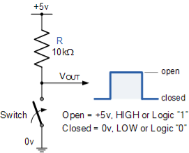
Fig 2 - Input Interfacing A Single Switch
Switches and push-buttons are mechanical devices that have two or more sets of electrical contacts. When the switch is open or disconnected, the contacts are open circuited and when the switch is closed or operated these contacts are shorted together.
The most common way of input interfacing a switch (or push button) to an electronic circuit is via a pull-up resistor to the supply voltage as shown. When the switch is open, 5 volts, or a logic “1” is given as the output signal. When the switch is closed the output is grounded and 0v, or a logic “0” is given as the output.
Then depending upon the position of the switch, a “high” or a “low” output is produced. A pull-up resistor is necessary to hold the output voltage level at the required value (in this example, +5v) when the switch is open and also to prevent the switch from shorting out the supply when closed.
The size of the pull-up resistor depends on the circuit current when the switch is open. For example, with the switch open, current will flow down through the resistor to the VOUT terminal and from Ohms Law this flow of current will cause a voltage drop to appear across the resistor.
Then if we assume a digital logic TTL gate requires an input “HIGH” current of 60 micro-amps (60uA), this causes a voltage drop across the resistor of: 60uA x 10kΩ = 0.6V, producing an input “HIGH” voltage of 5.0 - 0.6 = 4.4V which is well within the input specifications of a standard digital TTL gate.
A switch or push-button can also be connected in “active high” mode where the switch and resistor are reversed so that the switch is connected between the +5V supply voltage and the output. The resistor, which is now known as a pull-down resistor, is connected between the output and the 0v ground. In this configuration when the switch is open, the output signal, VOUT is at 0v, or logic “0”. When the witch is operated the output goes “HIGH” to the +5 volts supply voltage or logic “1”.
Unlike the pull-up resistor which is used to limit the current, the main purpose of a pull-down resistor is to keep the output terminal, VOUT from floating about by tying it to 0v or ground. As result a much smaller resistor can be used as the voltage drop across it will usually be very small. However, using a too small a pull-down resistor value will result in high currents and high-power dissipation in the resistor when the switch is closed or operated.
|
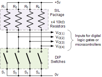
Fig 3 - DIP Switch Input Interfacing
As well as input interfacing individual push-buttons and rocker switches to circuits, we can also interface several switches together in the form of keypads and DIP switches.
DIP or Dual-in-line Package switches are individual switches that are grouped together as four or eight switches within a single package. This allows DIP switches to be inserted into standard IC sockets or wired directly onto a circuit or breadboard.
Each switch within a DIP switch package normally indicates one of two conditions by its ON-OFF status and a four switch DIP package will have four outputs as shown. Both slide and rotary type DIP switches can be connected together or in combinations of two or three switches which makes input interfacing them to a wide range of circuits very easy.
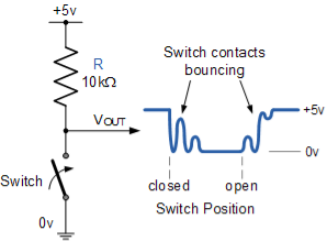
Mechanical switches are popular because of their low cost and ease of input interfacing. However, mechanical switches have a common problem called “contact bounce”. Mechanical switches consist of two pieces of metal contacts which are pushed together to complete a circuit when you operate the switch. But instead of producing a single clean switching action, the metal parts touch and bounce together inside the body of the switch causing the switching mechanism to open and close several times very quickly.
Because the mechanical switch contacts are designed to open and close quickly, there is very little resistance, called damping to stop the contacts from bouncing about as they make or break. The result is that this bouncing action produces a series of pulses or voltage spikes before the switch makes a solid contact.
|
Fig 4 - Switch Bounce Waveform
The problem is that any electronic or digital circuit which the mechanical switch is input interfaced too could read these multiple switch operations as a series of ON and OFF signals lasting several milliseconds instead of just the one intended single and positive switching action.
This multiple switch closing (or opening) action is called Switch Bounce in switches with the same action being called Contact Bounce in relays. Also, as switch and contact bounce occurs during both the opening and closing actions, the resultant bouncing and arcing across the contacts causes wear, increases contact resistance, and lowers the working life of the switch.
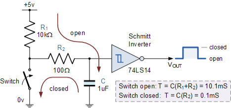
However, there are several ways in which we can solve this problem of switch bounce by using some extra circuitry in the form of a debounce circuit to “de-bounce” the input signal. The easiest and simplest way is to create an RC debounce circuit that allows the switch to charge and discharge a capacitor as shown.
|
Fig 5 - RC Switch Debounce Circuit
With the addition of an extra 100Ω resistor and a 1uF capacitor to the switches input interfacing circuit, the problems of switch bounce can be filtered out. The RC time constant, T is chosen to be longer than the bounce time of the mechanical switching action. An inverting Schmitt-trigger buffer can also be used to produce a sharp output transition from LOW to HIGH, and from HIGH to LOW.
So how does this type of input interfacing circuit work? Well, we saw in the RC Charging tutorial that a capacitor charges up at a rate determined by its time constant, T. This time constant value is measured in terms of T = R*C, in seconds, where R is the value of the resistor in Ohms and C is the value of the capacitor in Farads. This then forms the basis of an RC time constant.
Lets first assume that the switch is closed and the capacitor is fully discharged, then the input to the inverter is LOW and its output is HIGH. When the switch is opened, the capacitor charges up via the two resistors, R1 and R2 at a rate determined by the C(R1+R2) time constant of the RC network.
As the capacitor charges up slowly, any bouncing of the switch contacts are smoothed out by the voltage across the capacitor’s plates. When the charge on the plates is equal too or greater than the lowest value of the upper input voltage ( VIH ) of the inverter, the inverter changes state and the output becomes LOW. In this simple switch input interfacing example, the RC value is about 10mS giving the switch contacts enough time to settle into their final open state.
When the switch is closed, the now fully charged capacitor will quickly discharge to zero through the 100Ω at a rate determined by the C(R2) time constant changing the state of the inverters output from LOW to HIGH. However, the operation of the switch causes the contacts to bounce about resulting in the capacitor wanting to repeatedly charge up and then discharge rapidly back to zero.
Since the RC charging time constant is ten times longer than the discharge time constant, the capacitor cannot charge up fast enough before the switch bounces back to its final closed position as the input rise time has been slowed down, so the inverter keeps the output HIGH. The result is that no matter how much the switch contacts bounce when opening or closing, you will only get a single output pulse from the inverter.
The advantage of this simple switch debounce circuit is hat if the switch contacts bounce too much or fr too long the RC time constant can be increased to compensate. Also remember that this RC time delay means that you will need to wait before you can operate the switch again because if you operate the switch again too soon it will not generate another output signal.
While this simple switch debounce circuit will work for input interfacing single (SPST) switches to electronic and micro controller circuits, the disadvantage of the RC time constant is that it introduces a delay before the next switching action can occur. If the switching action changes state quickly, or multiple keys are operated as on a keypad, then this delay may be unacceptable. One way to overcome this problem and produce a faster input interfacing circuit is to use a cross coupled 2-input NAND or 2-input NOR gates as shown below.
|
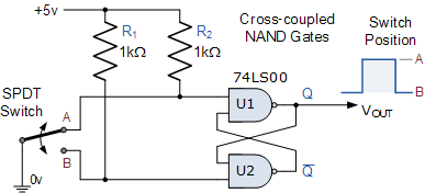
Fig 6 - Switch Debounce with NAND Gates
This type of switch debounce circuit operates in a very similar way to the SR Flip-flop we looked at in the Sequential Logic section. The two digital logic gates are connected as a pair of cross-coupled NAND gates with active LOW inputs forming a SR Latch circuit as two of the NAND gate inputs are held HIGH (+5v) by the two 1kΩ pull-up resistors as shown.
Also, as the circuit operates as a Set-Reset SR latch, the circuit requires a single-pole double-throw (SPDT) changeover switch rather than a single-pole single-throw (SPST) switch of the previous RC debounce circuit.
When the switch of the cross-coupled NAND debounce circuit is in position A, NAND gate U1 is “set” and the output at Q is HIGH at logic “1”. When the switch is moved to position B, U2 becomes “set” which resets U1. The output at Q is now LOW at logic “0”.
The operating the switch between positions A and B toggles or switches the output at Q from HIGH to LOW or from LOW to HIGH. As the latch requires two switching actions to set and reset it, any bouncing of the switch contacts in either direction for both opening and closing are not seen at the output Q. Also the advantage of this SR latch debounce circuit is that it can provide complementary outputs at Q and Q.
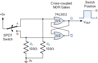
As well as using cross-coupled NAND gates to form a bistable latch input interfacing circuit, we can also use cross-coupled NOR gates by changing the position of the two resistors and reducing their value to 100Ω’s as shown below.
|
Fig 7 - Switch Debounce with NOR Gates
The operation of the cross-coupled NOR gate debounce circuit is the same as for the NAND circuit except that the output at Q is HIGH when the switch is in position B and LOW when it is in position A. The reverse of the cross-couple NAND bistable latch.
Then its worth noting that when input interfacing switches to circuits using a NAND or a NOR latch to use as debounce circuits, the NAND configuration requires a LOW or logic “0” input signal to change state, while the NOR configuration requires a HIGH or logic “1” input signal to change state.
An Optocoupler (or optoisolator) is an electronic component with an LED and photo-sensitive device, such as a photodiode or phototransistor encased in the same package. The Opto-coupler which we look at in a previous tutorial interconnects two separate electrical circuits by means of a light sensitive optical interface. This means that we can effectively interface two circuits of different voltage or power ratings together without one electrically affecting the other.
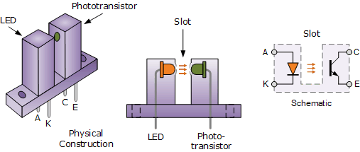
Optical Switches (or opto-switches) are another type of optical (photo) switching devices which can be used for input interfacing. The advantage here is that the optical switch can be used for input interfacing harmful voltage levels onto the input pins of microcontrollers, PICs and other such digital circuits or for detecting objects using light as the two components are electrically separate but optically coupled providing a high degree of isolation (typically 2-5kV).
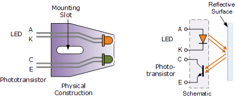
Optical switches come in a variety of different types and designs for use in a whole range of interfacing applications. The most common use for opto-switches is in the detection of moving or stationary objects. The phototransistor and photodarlington configurations provide most of the features required for photo-switches and are therefore the most commonly used.
|
Fig 8 - Slotted Optical Switch
A DC voltage is generally used to drive a light emitting diode (LED) which converts the input signal into infrared light energy. This light is reflected and collected by the phototransistor on the other side of the isolation gap and converted back into an output signal.
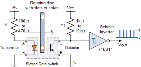
For normal opto-switches, the forward voltage drop of the LED is about 1.2 to 1.6 volts at a normal input current of 5 to 20 milliamperes. This gives a series resistor value of between 180 and 470Ω’s.
|
Fig 9 - Slotted Opto-switch Circuit
Rotary and slotted disk optical sensors are used extensively in positional encoders, shaft encoders and even the rotary wheel of your computer mouse and as such make excellent input interfacing devices. The rotary disk has a number of slots cut out of an opaque wheel with the number of evenly spaced slots representing the resolution per degree of rotation. Typical encoded discs have a resolution of up to 256 pulses or 8-bits per rotation.
During one revolution of the disk the infrared light from the LED strikes the phototransistor through the slot and then is blocked as the disk rotates, turning the transistor “ON” and then “OFF” each pass of the slot. Resistor R1 set the LED current and the pull-up resistor R2 ensures the supply voltage, Vcc is connected to the input of the Schmitt inverter when the transistor is “OFF” producing a LOW, logic “0” output.
When the disk rotates to an open cut out, the infrared light from the LED strikes the phototransistor and shorts the Collector-to-Emitter terminals to ground producing a LOW input to the Schmitt inverter which in turn outputs a HIGH or logic “1”. If the inverters output was connected to a digital counter or encoder, then it would be possible to determine the shafts position or count the numbers of shaft revolutions per unit time to give the shafts rotations per minute (rpm).
As well as using slotted opto devices as input interfacing switches, there is another type of optical device called a reflective optical sensor which uses an LED and photodevice to detect an object. The reflective opto switch can detect the absence or presence of an object by reflecting (hence its name) the LEDs infrared light of the reflective object being sensed. The basic arrangement of a reflective opto sensor is given below.
|
Fig 10 - Reflective Optical Switch
The phototransistor has a very high “OFF” resistance (dark) and a low “ON” resistance (light), which are controlled by the amount of light striking its base from the LED. If there is no object in front of the sensor then the LEDs infrared light will shine forward as a single beam. When there is an object in close proximity to the sensor the LEDs light is reflected back and detected by the phototransistor. The amount of reflected light sensed by the phototransistor and the degree of transistor saturation will depend on how close or reflective the object is.
As well as using slotted or reflective photo switches for the input interfacing of circuits, we can also use other types of semiconductor light detectors such as photo resistive light detectors, PN junction photodiodes and even solar cells. All these photo sensitive devices use ambient light such as sunlight or normal room light to activate the device allowing them to be easily interfaced to any type of electronic circuit.
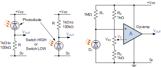
Normal signal and power diodes have their PN junction sealed within a plastic body for both safety and to stop photons of light from hitting it. When a diode is reverse biased it blocks the flow of current, acting like a high resistance open switch. However, if we were to shine a light onto this PN junction the photons of light open up the junction allowing current to flow depending upon the intensity of the light on the junction.
Photodiodes exploit this by having a small transparent window that allows light to strike their PN junction making the photodiode extremely photosensitive. Depending upon the type and amount of semiconductor doping, some photodiodes respond to visible light, and some to infra-red (IR) light. When there is no incident light, the reverse current, is almost negligible and is called the “dark current”. An increase in the amount of light intensity produces an increase in the reverse current.
Then we can see that a photodiode allows reverse current to flow in one direction only which is the opposite to a standard rectifying diode. This reverse current only flows when the photodiode receives a specific amount of light acting as very high impedances under dark conditions and as low impedance devices under bright light conditions and as such of the photodiode can be used in many applications as a high-speed light detector.
|
Fig 11 - Interfacing Photodiodes
In the two basic circuits on the left, the photodiode is simply reverse biased through the resistor with the output voltage signal taken from across the series resistor. This resistor can be of a fixed value, usually between the 10kΩ to 100kΩ range, or as a variable 100kΩ potentiometer as shown. This resistor can be connected between the photodiode and 0v ground, or between the photodiode and the positive Vcc supply.
While photodiodes such as the BPX48 give a very fast response to changes in light level, they can be less sensitive compared to other photo-devices such as the Cadmium Sulphide LDR cell so some form of amplification in the form of a transistor or op-amp may be required. Then we have seen that the photodiode can be used as a variable-resistive device controlled by the amount of light falling on its junction. Photodiodes can be switch from “ON” to “OFF” and back very fast sometimes in nano-seconds or with frequencies above 1MHz and so are commonly used in optical encoders and fibre optic communications.
As well as PN junction photo devices, such as the photodiode or the phototransistor, there are other types of semiconductor light detectors that operate without a PN junction and change their resistive characteristics with changes or variations in light intensity. These devices are called Light Dependant Resistors, or LDR’s.
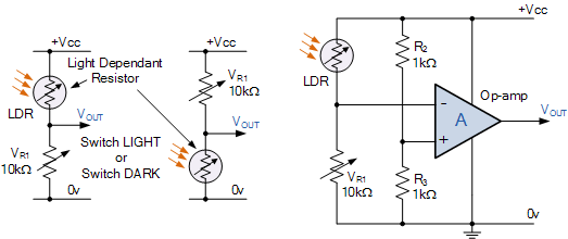
The LDR, also known as a cadmium-sulphide (CdS) photocell, is a passive device with a resistance that varies with visible light intensity. When no light is present their internal resistance is very high in the order of mega-ohms ( MΩ ). However, when illuminated their resistance falls to below 1kΩ in strong sunlight. Then light dependant resistors operate in a similar fashion to potentiometers but with light intensity controlling their resistive value.
|
Fig 12 - Interfacing LDR Photoresistors
Light dependant resistors change their resistive value in proportion to the light intensity. Then LDRs can be used with a series resistor, R to form a voltage divider network across the supply. In the dark the resistance of the LDR is much greater than that of the resistor so by connecting the LDR from supply to resistor or resistor to ground, it can be used as a light detector or as a dark detector as shown.
As LDRs such as the NORP12, produce a variable voltage output relative to their resistive value, they can be used for analogue input interfacing circuits. But LDRs can also be connected as part of a Wheatstone Bridge arrangement as the input of an op-amp voltage comparator or a Schmitt trigger circuit to produce a digital signal for interfacing to digital and microcontroller input circuits.
Simple threshold detectors for either light level, temperature or strain can be used to produce TTL compatible outputs suitable for interfacing directly to a logic circuit or digital input port. Light and temperature level threshold detectors based on an op-amp comparator generate a logic “1” or a logic “0” input whenever the measured level exceeds or falls below the threshold setting.
As we have seen throughout this tutorial section on input and output devices, there are many different types of sensors which can be used to convert one or more physical properties into an electrical signal that can then be used and processed by a suitable electronic, microcontroller or digital circuit.
The problem is that just about all of the physical properties being measured can not be directly connected to the processing or amplifying circuit. Then some form of input interfacing circuit is required to interface the wide range of different analogue input voltages and currents to a microprocessor digital circuit.
Today with modern PC’s, microcontrollers, PIC’s and other such microprocessor based systems, input interfacing circuits allows these low voltage, low power devices to easily communicate with the outside world as many of these PC based devices have built-in input–output ports for transferring data to and from the controllers program and attached switches or sensors.
We have seen that sensors are electrical components that convert one type of property into an electrical signal thereby functioning as input devices. Adding input sensors to an electronic circuit can expand its capabilities by providing information about the surrounding environment. However, sensors can not operate on their own and in the most cases an electrical or electronic circuit called an interface is required.
Then input interfacing circuits allow external devices to exchange signals (data or codes) from either simple switches using switch debounce techniques from a single push button or keyboard for data entry, to input sensors that can detect physical quantities such as light, temperature, pressure, and speed for conversion using analogue-to-digital converters. Then interfacing circuits allow us to do just that.
Key takeaways
- Interfacing is the method of connecting or linking together one device, especially a computer or micro-controller with another allowing us to design or adapt the output and input configurations of the two electronic devices so that they can work together.
- But interfacing is more than just using the software program of computers and processors to control something. While computer interfacing uses the unidirectional and bidirectional input and output ports to drive various peripheral devices, many simple electronic circuits can be used to interface to the real world either using mechanical switches as inputs, or individual LEDs as outputs.
Peripheral Component Interconnect (PCI)
PCI stands for Peripheral Component Interconnect.
It could be a standard information transport that was common in computers from 1993 to 2007 or so. It was for a long time the standard transport for extension cards in computers, like sound cards, network cards, etc. It was a parallel transport, that, in its most common shape, had a clock speed of 66 MHz, and can either be 32 or 64 bits wide. It has since been replaced by PCI Express, which could be a serial transport as contradicted to PCI. A PCI port, or, more precisely, PCI opening, is essentially the connector that’s utilized to put through the card to the transport. When purge, it basically sits there and does nothing.
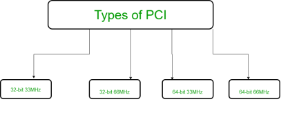
Types of PCI:
These are various types of PCI:
|
Fig 13 – Types of PCI
- PCI 32 bits have a transport speed of 33 MHz and work at 132 MBps.
- PCI 64 bits have a transport speed of 33 MHz and work at 264 MBps.
- PCI 64 bits have a transport speed of 66 MHz and work at 512 MBps.
- PCI 64 bits have a transport speed of 66 MHz and work at 1 GBps.
Function of PCI:
PCI slots are utilized to install sound cards, Ethernet and remote cards and presently strong state drives utilizing NVMe innovation to supply SSD drive speeds that are numerous times speedier than SATA SSD speeds. PCI openings too permit discrete design cards to be included to a computer as well.
PCI openings (and their variations) permit you to include expansion cards to a motherboard. The extension cards increment the machines capabilities past what the motherboard may create alone, such as: upgraded illustrations, extended sound, expanded USB and difficult drive controller, and extra arrange interface options, to title a couple of.
Advantage of PCI:
- You’ll interface a greatest of five components to the PCI and you’ll be able moreover supplant each of them by settled gadgets on the motherboard.
- You have different PCI buses on the same computer.
- The PCI transport will improve the speed of the exchanges from 33MHz to 133 MHz with a transfer rate of 1 gigabyte per second.
- The PCI can handle gadgets employing a greatest of 5 volts and the pins utilized can exchange more that one flag through one stick.
Disadvantage of PCI:
- PCI Graphics Card cannot get to to system memory.
- PCI does not support pipeline.
Small Computer System Interface
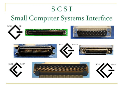
The basic interface for connecting peripheral devices to a PC is a small computer system interface. Based on the specification, it can typically respond up to 16 external devices using a single route, along with a host adapter. Small Computer System Interface is used to boost performance, deliver fast data transfer delivery and provide wider expansion for machines like CD-ROM drivers, scanners, DVD> drives and CD writers. Small Computer System Interface is most commonly used for RAID, servers, highly efficient desktop computers, and storage area networks. The Small Computer System Interface has control, which is responsible for transmitting data across the Small Computer System Interface bus and the computers. It can be fixed on a motherboard, or one client adapter is installed through an extension on the computer's motherboard. The controller also incorporates a simple SCSI input/output system, which is a small chip that provides access and control equipment with the necessary software. The SCSI ID is his number. Using serial storage architecture initiators, new serial SCSI IDs such as serial attached SCSI use an automatic process which assigns a 7-bit number.
|
Fig 14 - SCSI
SAS goods are compliant with appliances that use previous SCSI technology. The Serial Storage Architecture standard can be used if SCSI performance is not appropriate, as can iSCSI, which preserves the SCSI command set by embedding SCSI-3 over TCP/IP. In enterprise environments, SAS has become a common alternative to parallel SCSI. Serial and parallel small computer system interface are both based on the set of SCSI commands.
SAS provides the following unique benefits over parallel SCSI:
Through buses and interfaces, peripheral devices are connected to the CPU, and the most common interface for connecting these devices is SCSI. Compared to the parallel data transfer interfaces used in earlier days, SCSI was revolutionary technology in terms of data transfer and compatibility. SCSI also provides backward compatibility when systems are compliant with the previous SCSI edition. A modern variant of SCSI can also be connected to these machines, although the data transfer rate would be higher. A SCSI parallel bus was used for the original SCSI.
In 2008, the Serial SCSI architecture, which is faster and more stable than the parallel SCSI bus, was implemented. Internet SCSI used Internet protocol. This design does not have any physical features. It transmits data through TCP/IP. The Shugart Associates Machine Interface developed SCSI in 1978 and industrialized it in 1981. The founder of this technology was Larry Boucher, once employed for Shugart Associates, then subsequently for Adaptec, a company that produces SCSI, serial attached SCSI, and supporting host adapters. For data transmission, the SASI was developed as an interface between an HDD and a host PC. Utilizing an 8-bit parity bus, it had a 50-pin ribbon plug and supported up to 8 devices. The SASI sent data in blocks with a 5 MHz clock speed and ran asynchronously in synchronous mode at 3.5 MB/ps or 5 MB/ps.
By 2000, the Ultra 640 SCSI had a 160 MHz clock speed, creating parallel cabling problems. The serial SCSI was changed to fix the error. Device links are now hot-swappable plus compliant at a lower cost for serial advanced technology attachment. The clock speed increased to 4 GHz using the arbitrated fiber channel loop and optical fiber cables. Using one socket, the SCSI can support external and internal SCSI devices. There are usually two or three 50, 68 or 80 pin sockets for the internal parallel SCSI ribbon wire. A port is used by external devices. Depending on the SCSI bus standard, the external cable is always shielded and has 50 or 69 pin sockets on each end. There is also a single connector attachment, which contains two variations of an internal connection.
A single daisy chain is supported by both SCSI devices and the host adapter. In a sequence of nodes, a daisy chain ties the modules one after the other using a hardware setup. Depending on the SCSI version, the SCSI Graphic User Interface (GUI) supports different devices. A daisy chain's advantage is the ability to add an extra node anywhere on the chain. One or more signals may be modified by each unit in the chain before being sent to the next unit. Sixteen computers are supported by SCSI-2, 5 to 8 are supported by super SCSI, and 16 are supported by ultra-320 SCSI.
Universal Serial Bus (USB)
Universal Serial Bus (USB) is an industry standard that establishes specifications for connectors, cables and protocols for communication, connection and power supply between personal computers and their peripheral devices. There have been 3 generations of USB specifications:
1. USB 1.x
2. USB 2.0
3. USB 3.x
USB 2.0 have multiple updates and additions. The USB Implementer Forum (USB IF) currently maintains the USB standard and it was released in 1996.
USB was designed to standardize the connection of peripherals like pointing devices, keyboards, digital still and video cameras. But soon devices such as printers, portable media players, disk drives and network adaptors to personal computers used USB to communicate and to supply electric power. It is a commonplace to many devices and has largely replaced interfaces such as serial ports and parallel ports. USB connectors have replaced other types for battery chargers of portable devices with itself.
Advantages of USB –
The Universal Serial Bus was designed to simplify and improve the interface between personal computers and peripheral devices, when compared with previously existing standard or ad-hoc proprietary interfaces.
- The USB interface is self-configuring. This means that the user need not adjust settings on the device and interface for speed or data format, or configure interrupts, input/output addresses, or direct memory access channels.
- USB connectors are standardized at the host, so any peripheral can use any available receptacle. USB takes full advantage of the additional processing power that can be economically put into peripheral devices so that they can manage themselves. USB devices mostly do not have user-adjustable interface settings.
- The USB interface is hot pluggable or plug and play, meaning devices can be exchanged without rebooting the host computer. Small devices can be powered directly from the USB interface thus removing extra power supply cables.
- The USB interface defines protocols for improving reliability over previous interfaces and recovery from common errors.
- Installation of a device relying on the USB standard minimal operator action is required.
Disadvantages of USB –
- USB cables are limited in length.
- USB has a strict “tree” topology and “master-slave” protocol for addressing peripheral devices. Peripheral devices cannot interact with one another except via the host, and two hosts cannot communicate over their USB ports directly.
- Some very high speed peripheral devices require sustained speeds not available in the USB standard.
- For a product developer, use of USB requires implementation of a complex protocol and implies an intelligent controller in the peripheral device.
- Use of the USB logos on the product require annual fees and membership in the organization.
Key takeaways
- It could be a standard information transport that was common in computers from 1993 to 2007 or so. It was for a long time the standard transport for extension cards in computers, like sound cards, network cards, etc. It was a parallel transport, that, in its most common shape, had a clock speed of 66 MHz, and can either be 32 or 64 bits wide. It has since been replaced by PCI Express, which could be a serial transport as contradicted to PCI. A PCI port, or, more precisely, PCI opening, is essentially the connector that’s utilized to put through the card to the transport. When purge, it basically sits there and does nothing.
References
1. William Stallings: Computer Organization & Architecture, 7th Edition, PHI, 2006.
2. Vincent P. Heuring & Harry F. Jordan: Computer Systems Design and Architecture, 2 nd Edition, Pearson Education, 2004.
