A memory unit is an essential component in any digital computer since it is needed for storing programs and data.
Typically, a memory unit can be classified into two categories:
- The memory unit that establishes direct communication with the CPU is called Main Memory. The main memory is often referred to as RAM (Random Access Memory).
- The memory units that provide backup storage are called Auxiliary Memory. For instance, magnetic disks and magnetic tapes are the most commonly used auxiliary memories.
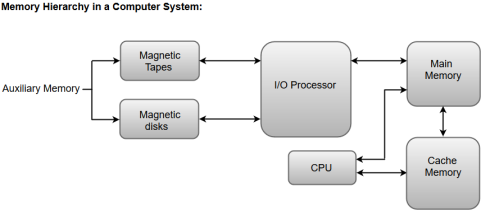
Apart from the basic classifications of a memory unit, the memory hierarchy consists all of the storage devices available in a computer system ranging from the slow but high-capacity auxiliary memory to relatively faster main memory.
The following image illustrates the components in a typical memory hierarchy.
|
Fig 1 – Memory hierarchy in a computer system
Auxiliary Memory
Auxiliary memory is known as the lowest-cost, highest-capacity and slowest-access storage in a computer system. Auxiliary memory provides storage for programs and data that are kept for long-term storage or when not in immediate use. The most common examples of auxiliary memories are magnetic tapes and magnetic disks.
A magnetic disk is a digital computer memory that uses a magnetization process to write, rewrite and access data. For example, hard drives, zip disks, and floppy disks.
Magnetic tape is a storage medium that allows for data archiving, collection, and backup for different kinds of data.
The main memory in a computer system is often referred to as Random Access Memory (RAM). This memory unit communicates directly with the CPU and with auxiliary memory devices through an I/O processor.
The programs that are not currently required in the main memory are transferred into auxiliary memory to provide space for currently used programs and data.
The primary function of an I/O Processor is to manage the data transfers between auxiliary memories and the main memory.
The data or contents of the main memory that are used frequently by CPU are stored in the cache memory so that the processor can easily access that data in a shorter time. Whenever the CPU requires accessing memory, it first checks the required data into the cache memory. If the data is found in the cache memory, it is read from the fast memory. Otherwise, the CPU moves onto the main memory for the required data.
The main memory acts as the central storage unit in a computer system. It is a relatively large and fast memory which is used to store programs and data during the run time operations.
The primary technology used for the main memory is based on semiconductor integrated circuits. The integrated circuits for the main memory are classified into two major units.
- RAM (Random Access Memory) integrated circuit chips
- ROM (Read Only Memory) integrated circuit chips
The RAM integrated circuit chips are further classified into two possible operating modes, static and dynamic.
The primary compositions of a static RAM are flip-flops that store the binary information. The nature of the stored information is volatile, i.e. it remains valid as long as power is applied to the system. The static RAM is easy to use and takes less time performing read and write operations as compared to dynamic RAM.
The dynamic RAM exhibits the binary information in the form of electric charges that are applied to capacitors. The capacitors are integrated inside the chip by MOS transistors. The dynamic RAM consumes less power and provides large storage capacity in a single memory chip.
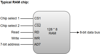
RAM chips are available in a variety of sizes and are used as per the system requirement. The following block diagram demonstrates the chip interconnection in a 128 * 8 RAM chip.
|
Fig 2 – Typical RAM chip
- A 128 * 8 RAM chip has a memory capacity of 128 words of eight bits (one byte) per word. This requires a 7-bit address and an 8-bit bidirectional data bus.
- The 8-bit bidirectional data bus allows the transfer of data either from memory to CPU during a read operation or from CPU to memory during a write operation.
- The read and write inputs specify the memory operation, and the two chip select (CS) control inputs are for enabling the chip only when the microprocessor selects it.
- The bidirectional data bus is constructed using three-state buffers.
- The output generated by three-state buffers can be placed in one of the three possible states which include a signal equivalent to logic 1, a signal equal to logic 0, or a high-impedance state.
Note: The logic 1 and 0 are standard digital signals whereas the high-impedance state behaves like an open circuit, which means that the output does not carry a signal and has no logic significance.
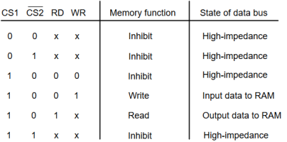
The following function table specifies the operations of a 128 * 8 RAM chip.
|
From the functional table, we can conclude that the unit is in operation only when CS1 = 1 and CS2 = 0. The bar on top of the second select variable indicates that this input is enabled when it is equal to 0.
The primary component of the main memory is RAM integrated circuit chips, but a portion of memory may be constructed with ROM chips.
A ROM memory is used for keeping programs and data that are permanently resident in the computer.
Apart from the permanent storage of data, the ROM portion of main memory is needed for storing an initial program called a bootstrap loader. The primary function of the bootstrap loader program is to start the computer software operating when power is turned on.
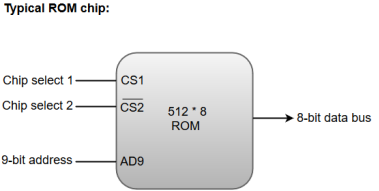
ROM chips are also available in a variety of sizes and are also used as per the system requirement. The following block diagram demonstrates the chip interconnection in a 512 * 8 ROM chip.
|
Fig 3 – Typical ROM chip
- A ROM chip has a similar organization as a RAM chip. However, a ROM can only perform read operation; the data bus can only operate in an output mode.
- The 9-bit address lines in the ROM chip specify any one of the 512 bytes stored in it.
- The value for chip select 1 and chip select 2 must be 1 and 0 for the unit to operate. Otherwise, the data bus is said to be in a high-impedance state.
Key takeaways
- A memory unit is an essential component in any digital computer since it is needed for storing programs and data.
- Typically, a memory unit can be classified into two categories:
- The memory unit that establishes direct communication with the CPU is called Main Memory. The main memory is often referred to as RAM (Random Access Memory).
- The memory units that provide backup storage are called Auxiliary Memory. For instance, magnetic disks and magnetic tapes are the most commonly used auxiliary memories.
Semiconductor memory is used in any electronics assembly that uses computer processing technology. Semiconductor memory is the essential electronics component needed for any computer-based PCB assembly.
In addition to this, memory cards have become commonplace items for temporarily storing data - everything from the portable flash memory cards used for transferring files, to semiconductor memory cards used in cameras, mobile phones and the like.
The use of semiconductor memory has grown, and the size of these memory cards has increased as the need for larger and larger amounts of storage is needed.
To meet the growing needs for semiconductor memory, there are many types and technologies that are used. As the demand grows new memory technologies are being introduced and the existing types and technologies are being further developed.
A variety of different memory technologies are available - each one suited to different applications. Names such as ROM, RAM, EPROM, EEPROM, Flash memory, DRAM, SRAM, SDRAM, as well as F-RAM and MRAM are available, and new types are being developed to enable improved performance.
Terms like DDR3, DDR4, DDR5 and many more are seen and these refer to different types of SDRAM semiconductor memory.
In addition to this the semiconductor devices are available in many forms - ICs for printed board assembly, USB memory cards, Compact Flash cards, SD memory cards and even solid-state hard drives. Semiconductor memory is even incorporated into many microprocessor chips as on-board memory.
|
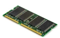
Fig 4 - Printed circuit board containing computer memory
Semiconductor memory: main types
There are two main types or categories that can be used for semiconductor technology. These memory types or categories differentiate the memory to the way in which it operates:
RAM - Random Access Memory: As the names suggest, the RAM or random-access memory is a form of semiconductor memory technology that is used for reading and writing data in any order - in other words as it is required by the processor. It is used for such applications as the computer or processor memory where variables and other stored and are required on a random basis. Data is stored and read many times to and from this type of memory.
Random access memory is used in huge quantities in computer applications as current day computing and processing technology requires large amounts of memory to enable them to handle the memory hungry applications used today. Many types of RAM including SDRAM with its DDR3, DDR4, and soon DDR5 variants are used in huge quantities.
ROM - Read Only Memory: A ROM is a form of semiconductor memory technology used where the data is written once and then not changed. In view of this it is used where data needs to be stored permanently, even when the power is removed - many memory technologies lose the data once the power is removed.
As a result, this type of semiconductor memory technology is widely used for storing programs and data that must survive when a computer or processor is powered down. For example, the BIOS of a computer will be stored in ROM. As the name implies, data cannot be easily written to ROM. Depending on the technology used in the ROM, writing the data into the ROM initially may require special hardware. Although it is often possible to change the data, this gain requires special hardware to erase the data ready for new data to be written in.
As can be seen, these two types of memory are very different, and as a result they are used in very different ways.
Each of the semiconductor memory technologies outlined below falls into one of these two types of category. each technology offers its own advantages and is used in a particular way, or for a particular application.
Semiconductor memory technologies
There is a large variety of types of ROM and RAM that are available. Often the overall name for the memory technology includes the initials RAM or ROM and this gives a guide as to the overall type of format for the memory.
With technology moving forwards apace, not only are the established technologies moving forwards with SDRAM technology moving from DDR3 to DDR4 and then to DDR5, but Flash memory used in memory cards is also developing as are the other technologies.
In addition to this, new memory technologies are arriving on the scene and they are starting to make an impact in the market, enabling processor circuits to perform more effectively.
The different memory types or memory technologies are detailed below:
DRAM: Dynamic RAM is a form of random-access memory. DRAM uses a capacitor to store each bit of data, and the level of charge on each capacitor determines whether that bit is a logical 1 or 0. However these capacitors do not hold their charge indefinitely, and therefore the data needs to be refreshed periodically. As a result of this dynamic refreshing, it gains its name of being a dynamic RAM. DRAM is the form of semiconductor memory that is often used in equipment including personal computers and workstations where it forms the main RAM for the computer. The semiconductor devices are normally available as integrated circuits for use in PCB assembly in the form of surface mount devices or less frequently now as leaded components.
EEPROM: This is an Electrically Erasable Programmable Read Only Memory. Data can be written to these semiconductor devices and it can be erased using an electrical voltage. This is typically applied to an erase pin on the chip. Like other types of PROM, EEPROM retains the contents of the memory even when the power is turned off. Also, like other types of ROM, EEPROM is not as fast as RAM.
EPROM: This is an Erasable Programmable Read Only Memory. These semiconductor devices can be programmed and then erased at a later time. This is normally achieved by exposing the semiconductor device itself to ultraviolet light. To enable this to happen there is a circular window in the package of the EPROM to enable the light to reach the silicon of the device. When the PROM is in use, this window is normally covered by a label, especially when the data may need to be preserved for an extended period. The PROM stores its data as a charge on a capacitor. There is a charge storage capacitor for each cell and this can be read repeatedly as required. However, it is found that after many years the charge may leak away and the data may be lost. Nevertheless, this type of semiconductor memory used to be widely used in applications where a form of ROM was required, but where the data needed to be changed periodically, as in a development environment, or where quantities were low.
Flash memory: Flash memory may be considered as a development of EEPROM technology. Data can be written to it and it can be erased, although only in blocks, but data can be read on an individual cell basis.
To erase and re-programme areas of the chip, programming voltages at levels that are available within electronic equipment are used. It is also non-volatile, and this makes it particularly useful. As a result, Flash memory is widely used in many applications including USB memory sticks, compact Flash memory cards, SD memory cards and also now solid-state hard drives for computers and many other applications.
F-RAM: Ferroelectric RAM is a random-access memory technology that has many similarities to the standard DRAM technology. The major difference is that it incorporates a ferroelectric layer instead of the more usual dielectric layer and this provides its non-volatile capability. As it offers a non-volatile capability, F-RAM is a direct competitor to Flash.
MRAM: This is Magneto-resistive RAM, or Magnetic RAM. It is a non-volatile RAM memory technology that uses magnetic charges to store data instead of electric charges.
Unlike technologies including DRAM, which require a constant flow of electricity to maintain the integrity of the data, MRAM retains data even when the power is removed. An additional advantage is that it only requires low power for active operation. As a result, this technology could become a major player in the electronics industry now that production processes have been developed to enable it to be produced.
P-RAM / PCM: This type of semiconductor memory is known as Phase change Random Access Memory, P-RAM or just Phase Change memory, PCM. It is based around a phenomenon where a form of chalcogenide glass changes is state or phase between an amorphous state (high resistance) and a polycrystalline state (low resistance). It is possible to detect the state of an individual cell and hence use this for data storage. Currently this type of memory has not been widely commercialised, but it is expected to be a competitor for flash memory.
PROM: This stands for Programmable Read Only Memory. It is a semiconductor memory which can only have data written to it once - the data written to it is permanent. These memories are bought in a blank format and they are programmed using a special PROM programmer.
Typically, a PROM will consist of an array of fuseable links some of which are "blown" during the programming process to provide the required data pattern.
SDRAM: Synchronous DRAM. This form of semiconductor memory can run at faster speeds than conventional DRAM. It is synchronised to the clock of the processor and is capable of keeping two sets of memory addresses open simultaneously. By transferring data alternately from one set of addresses, and then the other, SDRAM cuts down on the delays associated with non-synchronous RAM, which must close one address bank before opening the next.
Within the SDRAM family there are several types of memory technologies that are seen. These are referred to by the letters DDR - Double Data Rate. DDR4 is currently the latest technology, but this is soon to be followed by DDR5 which will offer some significant improvements in performance.
SRAM: Static Random-Access Memory. This form of semiconductor memory gains its name from the fact that, unlike DRAM, the data does not need to be refreshed dynamically.
These semiconductor devices are able to support faster read and write times than DRAM (typically 10 ns against 60 ns for DRAM), and in addition its cycle time is much shorter because it does not need to pause between accesses. However, they consume more power, they are less dense and more expensive than DRAM. As a result of this SRAM is normally used for caches, while DRAM is used as the main semiconductor memory technology.
Semiconductor memory technology is developing at a fast rate to meet the ever-growing needs of the electronics industry. Not only are the existing technologies themselves being developed, but considerable amounts of research are being invested in new types of semiconductor memory technology.
In terms of the memory technologies currently in use, SDRAM versions like DDR4 are being further developed to provide DDR5 which will offer significant performance improvements. In time, DDR5 will be developed to provide the next generation of SDRAM.
Other forms of memory are seen around the home in the form of USB memory sticks, Compact Flash, CF cards or SD memory cards for cameras and other applications as well as solid state hard drives for computers.
The semiconductor devices are available in a wide range of formats to meet the differing PCB assembly and other needs.
Key takeaways
- Semiconductor memory is used in any electronics assembly that uses computer processing technology. Semiconductor memory is the essential electronics component needed for any computer-based PCB assembly.
- In addition to this, memory cards have become commonplace items for temporarily storing data - everything from the portable flash memory cards used for transferring files, to semiconductor memory cards used in cameras, mobile phones and the like.
- The use of semiconductor memory has grown, and the size of these memory cards has increased as the need for larger and larger amounts of storage is needed.
- To meet the growing needs for semiconductor memory, there are many types and technologies that are used. As the demand grows new memory technologies are being introduced and the existing types and technologies are being further developed.
|
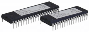
Fig 5 - ROM
ROM, which stands for read only memory, is a memory device or storage medium that stores information permanently. It is also the primary memory unit of a computer along with the random access memory (RAM). It is called read only memory as we can only read the programs and data stored on it but cannot write on it. It is restricted to reading words that are permanently stored within the unit.
The manufacturer of ROM fills the programs into the ROM at the time of manufacturing the ROM. After this, the content of the ROM can't be altered, which means you can't reprogram, rewrite, or erase its content later. However, there are some types of ROM where you can modify the data.
ROM contains special internal electronic fuses that can be programmed for a specific interconnection pattern (information). The binary information stored in the chip is specified by the designer and then embedded in the unit at the time of manufacturing to form the required interconnection pattern (information). Once the pattern (information) is established, it stays within the unit even when the power is turned off. So, it is a non-volatile memory as it holds the information even when the power is turned off, or you shut down your computer.
The information is added to a RAM in the form of bits by a process known as programming the ROM as bits are stored in the hardware configuration of the device. So, ROM is a Programmable Logic Device (PLD).
A simple example of ROM is the cartridge used in video game consoles that allows the system to run many games. The data which is stored permanently on personal computers and other electronic devices like smartphones, tablets, TV, AC, etc. is also an example of ROM.
For example, when you start your computer, the screen does not appear instantly. It takes time to appear as there are startup instructions stored in ROM which are required to start the computer during the booting process. The work of the booting process is to start the computer. It loads the operating system into the main memory (RAM) installed on your computer. The BIOS program, which is also present in the computer memory (ROM) is used by the microprocessor of the computer to start the computer during the booting process. It allows you to open the computer and connects the computer with the operating system.
ROM is also used to store Firmware, which is a software program which remains attached to the hardware or programmed on a hardware device like a keyboard, hard drive, video cards, etc. It is stored in the flash ROM of a hardware device. It provides instructions to the device to communicate and interact with other devices.
|
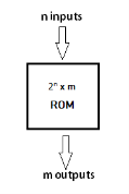
Fig 6 - Block Diagram of ROM
The block of ROM has 'n' input lines and 'm' output lines. Each bit combination of the input variables is known as an address. Each bit combination that comes out through output lines is called a word. The number of bits per word is equal to the number of output lines, m.
The address of a binary number refers to one of the addresses of n variables. So, the number of possible addresses with 'n' input variables is 2n. An output word has a unique address, and as there are 2n distinct addresses in a ROM, there are 2n separate words in the ROM. The words on the output lines at a given time depends on the address value applied to the input lines.
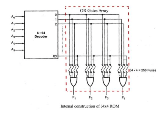
The internal structure comprises two basic components: decoder and OR gates. A decoder is a circuit that decodes an encoded form (such as binary coded decimal, BCD) to a decimal form. So, the input is in binary form, and the output is its decimal equivalent. All the OR gates present in the ROM will have outputs of the decoder as their output. Let us take an example of 64 x 4 ROM. The structure is shown in the following image.
|
Fig 7 –Internal construction
This Read Only Memory consists of 64 words of 4 bits each. So, there would be four output lines, and one of the 64 words available on the output lines is determined from the six input lines as we have only six inputs because in this ROM we have 26 = 64, so we can specify 64 addresses or minterms. For each address input, there is a unique selected word. For example, if the input address is 000000, word number 0 will be selected and applied to the output lines. If the input address is 111111, word number 63 is selected and applied to the output lines.
1) Masked Read Only Memory (MROM):
It is the oldest type of read only memory (ROM). It has become obsolete so it is not used anywhere in today's world. It is a hardware memory device in which programs and instructions are stored at the time of manufacturing by the manufacturer. So it is programmed during the manufacturing process and can't be modified, reprogrammed, or erased later.
The MROM chips are made of integrated circuits. Chips send a current through a particular input-output pathway determined by the location of fuses among the rows and columns on the chip. The current has to pass along a fuse-enabled path, so it can return only via the output the manufacturer chooses. This is the reason the rewriting and any other modification is not impossible in this memory.
2) Programmable Read Only Memory (PROM):
PROM is a blank version of ROM. It is manufactured as blank memory and programmed after manufacturing. We can say that it is kept blank at the time of manufacturing. You can purchase and then program it once using a special tool called a programmer.
In the chip, the current travels through all possible pathways. The programmer can choose one particular path for the current by burning unwanted fuses by sending a high voltage through them. The user has the opportunity to program it or to add data and instructions as per his requirement. Due to this reason, it is also known as the user-programmed ROM as a user can program it.
To write data onto a PROM chip; a device called PROM programmer or PROM burner is used. The process or programming a PROM is known as burning the PROM. Once it is programmed, the data cannot be modified later, so it is also called as one-time programmable device.
Uses: It is used in cell phones, video game consoles, medical devices, RFID tags, and more.
3) Erasable and Programmable Read Only Memory (EPROM):
EPROM is a type of ROM that can be reprogramed and erased many times. The method to erase the data is very different; it comes with a quartz window through which a specific frequency of ultraviolet light is passed for around 40 minutes to erase the data. So, it retains its content until it is exposed to the ultraviolet light. You need a special device called a PROM programmer or PROM burner to reprogram the EPROM.
Uses: It is used in some micro-controllers to store program, e.g., some versions of Intel 8048 and the Freescale 68HC11.
4) Electrically Erasable and Programmable Read Only Memory (EEPROM):
ROM is a type of read only memory that can be erased and reprogrammed repeatedly, up to 10000 times. It is also known as Flash EEPROM as it is similar to flash memory. It is erased and reprogrammed electrically without using ultraviolet light. Access time is between 45 and 200 nanoseconds.
The data in this memory is written or erased one byte at a time; byte per byte, whereas, in flash memory data is written and erased in blocks. So, it is faster than EEPROM. It is used for storing a small amount of data in computer and electronic systems and devices such as circuit boards.
Uses: The BIOS of a computer is stored in this memory.
It is an advanced version of EEPROM. It stores information in an arrangement or array of memory cells made from floating-gate transistors. The advantage of using this memory is that you can delete or write blocks of data around 512 bytes at a particular time. Whereas, in EEPROM, you can delete or write only 1 byte of data at a time. So, this memory is faster than EEPROM.
It can be reprogrammed without removing it from the computer. Its access time is very high, around 45 to 90 nanoseconds. It is also highly durable as it can bear high temperature and intense pressure.
Uses: It is used for storage and transferring data between a personal computer and digital devices. It is used in USB flash drives, MP3 players, digital cameras, modems and solid-state drives (SSDs). The BIOS of many modern computers are stored on a flash memory chip, called flash BIOS.
Key takeaways
- ROM, which stands for read only memory, is a memory device or storage medium that stores information permanently. It is also the primary memory unit of a computer along with the random-access memory (RAM). It is called read only memory as we can only read the programs and data stored on it but cannot write on it. It is restricted to reading words that are permanently stored within the unit.
- The manufacturer of ROM fills the programs into the ROM at the time of manufacturing the ROM. After this, the content of the ROM can't be altered, which means you can't reprogram, rewrite, or erase its content later. However, there are some types of ROM where you can modify the data.
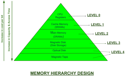
In the Computer System Design, Memory Hierarchy is an enhancement to organize the memory such that it can minimize the access time. The Memory Hierarchy was developed based on a program behaviour known as locality of references. The figure below clearly demonstrates the different levels of memory hierarchy:
|
Fig 8 – Memory hierarchy design
This Memory Hierarchy Design is divided into 2 main types:
- External Memory or Secondary Memory –
Comprising of Magnetic Disk, Optical Disk, Magnetic Tape i.e. peripheral storage devices which are accessible by the processor via I/O Module.
2. Internal Memory or Primary Memory –
Comprising of Main Memory, Cache Memory & CPU registers. This is directly accessible by the processor.
We can infer the following characteristics of Memory Hierarchy Design from above figure:
- Capacity:
It is the global volume of information the memory can store. As we move from top to bottom in the Hierarchy, the capacity increases.
2. Access Time:
It is the time interval between the read/write request and the availability of the data. As we move from top to bottom in the Hierarchy, the access time increases.
3. Performance:
Earlier when the computer system was designed without Memory Hierarchy design, the speed gap increases between the CPU registers and Main Memory due to large difference in access time. This results in lower performance of the system and thus, enhancement was required. This enhancement was made in the form of Memory Hierarchy Design because of which the performance of the system increases. One of the most significant ways to increase system performance is minimizing how far down the memory hierarchy one has to go to manipulate data.
4. Cost per bit:
As we move from bottom to top in the Hierarchy, the cost per bit increases i.e., Internal Memory is costlier than External Memory.
Key takeaways
- External Memory or Secondary Memory –
Comprising of Magnetic Disk, Optical Disk, Magnetic Tape i.e. peripheral storage devices which are accessible by the processor via I/O Module.
2. Internal Memory or Primary Memory –
Comprising of Main Memory, Cache Memory & CPU registers. This is directly accessible by the processor.
Cache Memory is a special very high-speed memory. It is used to speed up and synchronizing with high-speed CPU. Cache memory is costlier than main memory or disk memory but economical than CPU registers. Cache memory is an extremely fast memory type that acts as a buffer between RAM and the CPU. It holds frequently requested data and instructions so that they are immediately available to the CPU when needed.
Cache memory is used to reduce the average time to access data from the Main memory. The cache is a smaller and faster memory which stores copies of the data from frequently used main memory locations. There are various different independent caches in a CPU, which store instructions and data.
|
Fig 9 – Cache memory
Levels of memory:
Level 1 or Register –
It is a type of memory in which data is stored and accepted that are immediately stored in CPU. Most commonly used register is accumulator, Program counter, address register etc.
Level 2 or Cache memory –
It is the fastest memory which has faster access time where data is temporarily stored for faster access.
Level 3 or Main Memory –
It is memory on which computer works currently. It is small in size and once power is off data no longer stays in this memory.
Level 4 or Secondary Memory –
It is external memory which is not as fast as main memory but data stays permanently in this memory.
Cache Performance:
When the processor needs to read or write a location in main memory, it first checks for a corresponding entry in the cache.
If the processor finds that the memory location is in the cache, a cache hit has occurred and data is read from cache
If the processor does not find the memory location in the cache, a cache miss has occurred. For a cache miss, the cache allocates a new entry and copies in data from main memory, then the request is fulfilled from the contents of the cache.
The performance of cache memory is frequently measured in terms of a quantity called Hit ratio.
Hit ratio = hit / (hit + miss) = no. of hits/total accesses
We can improve Cache performance using higher cache block size, higher associativity, reduce miss rate, reduce miss penalty, and reduce the time to hit in the cache.
Cache Mapping:
There are three different types of mapping used for the purpose of cache memory which are as follows: Direct mapping, Associative mapping, and Set-Associative mapping. These are explained below.
Direct Mapping –
The simplest technique, known as direct mapping, maps each block of main memory into only one possible cache line. or
In Direct mapping, assign each memory block to a specific line in the cache. If a line is previously taken up by a memory block when a new block needs to be loaded, the old block is trashed. An address space is split into two parts index field and a tag field. The cache is used to store the tag field whereas the rest is stored in the main memory. Direct mappings performance is directly proportional to the Hit ratio.
i = j modulo m
where
i=cache line number
j= main memory block number
m=number of lines in the cache
For purposes of cache access, each main memory address can be viewed as consisting of three fields. The least significant w bits identify a unique word or byte within a block of main memory. In most contemporary machines, the address is at the byte level. The remaining s bits specify one of the 2s blocks of main memory. The cache logic interprets these s bits as a tag of s-r bits (most significant portion) and a line field of r bits. This latter field identifies one of the m=2r lines of the cache.
|
Fig 10 – Memory pages
Associative Mapping –
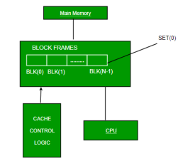
In this type of mapping, the associative memory is used to store content and addresses of the memory word. Any block can go into any line of the cache. This means that the word id bits are used to identify which word in the block is needed, but the tag becomes all of the remaining bits. This enables the placement of any word at any place in the cache memory. It is considered to be the fastest and the most flexible mapping form.
|
Fig 11 – Main memory example
Set-associative Mapping –
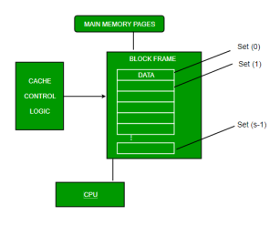
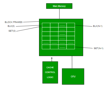
This form of mapping is an enhanced form of direct mapping where the drawbacks of direct mapping are removed. Set associative addresses the problem of possible thrashing in the direct mapping method. It does this by saying that instead of having exactly one line that a block can map to in the cache, we will group a few lines together creating a set. Then a block in memory can map to any one of the lines of a specific set..Set-associative mapping allows that each word that is present in the cache can have two or more words in the main memory for the same index address. Set associative cache mapping combines the best of direct and associative cache mapping techniques.
In this case, the cache consists of a number of sets, each of which consists of a number of lines. The relationships are
m = v * k i= j mod v where i=cache set number j=main memory block number v=number of sets m=number of lines in the cache number of sets k=number of lines in each set |
|
Fig 12 - Example
Application of Cache Memory –
Usually, the cache memory can store a reasonable number of blocks at any given time, but this number is small compared to the total number of blocks in the main memory.
The correspondence between the main memory blocks and those in the cache is specified by a mapping function.
Types of Cache
Primary Cache –
A primary cache is always located on the processor chip. This cache is small and its access time is comparable to that of processor registers.
Secondary Cache –
Secondary cache is placed between the primary cache and the rest of the memory. It is referred to as the level 2 (L2) cache. Often, the Level 2 cache is also housed on the processor chip.
Locality of reference –
Since size of cache memory is less as compared to main memory. So to check which part of main memory should be given priority and loaded in cache is decided based on locality of reference.
Types of Locality of reference
Spatial Locality of reference
This says that there is a chance that element will be present in the close proximity to the reference point and next time if again searched then more close proximity to the point of reference.
Temporal Locality of reference
In this Least recently used algorithm will be used. Whenever there is page fault occurs within a word will not only load word in main memory but complete page fault will be loaded because spatial locality of reference rule says that if you are referring any word next word will be referred in its register that’s why we load complete page table so the complete block will be loaded.
Key takeaways
1. Cache Memory is a special very high-speed memory. It is used to speed up and synchronizing with high-speed CPU. Cache memory is costlier than main memory or disk memory but economical than CPU registers. Cache memory is an extremely fast memory type that acts as a buffer between RAM and the CPU. It holds frequently requested data and instructions so that they are immediately available to the CPU when needed.
The page replacement algorithm decides which memory page is to be replaced. The process of replacement is sometimes called swap out or write to disk. Page replacement is done when the requested page is not found in the main memory (page fault).
|
Fig 13 – Virtual Memory
There are two main aspects of virtual memory, Frame allocation and Page Replacement. It is very important to have the optimal frame allocation and page replacement algorithm. Frame allocation is all about how many frames are to be allocated to the process while the page replacement is all about determining the page number which needs to be replaced in order to make space for the requested page.
What If the algorithm is not optimal?
1. if the number of frames which are allocated to a process is not sufficient or accurate then there can be a problem of thrashing. Due to the lack of frames, most of the pages will be residing in the main memory and therefore more page faults will occur.
However, if OS allocates more frames to the process then there can be internal fragmentation.
2. If the page replacement algorithm is not optimal then there will also be the problem of thrashing. If the number of pages that are replaced by the requested pages will be referred in the near future then there will be more number of swap-in and swap-out and therefore the OS has to perform more replacements then usual which causes performance deficiency.
Therefore, the task of an optimal page replacement algorithm is to choose the page which can limit the thrashing.
Types of Page Replacement Algorithms
There are various page replacement algorithms. Each algorithm has a different method by which the pages can be replaced.
- Optimal Page Replacement algorithm → this algorithm replaces the page which will not be referred for so long in future. Although it cannot be practically implementable but it can be used as a benchmark. Other algorithms are compared to this in terms of optimality.
- Least recent used (LRU) page replacement algorithm → this algorithm replaces the page which has not been referred for a long time. This algorithm is just opposite to the optimal page replacement algorithm. In this, we look at the past instead of staring at future.
- FIFO → in this algorithm, a queue is maintained. The page which is assigned the frame first will be replaced first. In other words, the page which resides at the rare end of the queue will be replaced on the every page fault.
Key takeaways
1. The page replacement algorithm decides which memory page is to be replaced. The process of replacement is sometimes called swap out or write to disk. Page replacement is done when the requested page is not found in the main memory (page fault).
Computer performance is the amount of work accomplished by a computer system. The word performance in computer performance means “How well is the computer doing the work it is supposed to do?”. It basically depends on response time, throughput and execution time of a computer system.
Response time is the time from start to completion of a task. This also includes:
- Operating system overhead.
- Waiting for I/O and other processes
- Accessing disk and memory
- Time spent executing on the CPU or execution time.
Throughput is the total amount of work done in a given time.
CPU execution time is the total time a CPU spends computing on a given task. It also excludes time for I/O or running other programs. This is also referred to as simply CPU time.
Performance is determined by execution time as performance is inversely proportional to execution time.
Performance = (1 / Execution time) And, (Performance of A / Performance of B) = (Execution Time of B / Execution Time of A) |
If given that Processor A is faster than processor B, that means execution time of A is less than that of execution time of B. Therefore, performance of A is greater than that of performance of B.
Example –
Machine A runs a program in 100 seconds, Machine B runs the same program in 125 seconds (Performance of A / Performance of B) = (Execution Time of B / Execution Time of A) = 125 / 100 = 1.25 That means machine A is 1.25 times faster than Machine B. And, the time to execute a given program can be computed as: Execution time = CPU clock cycles x clock cycle time Since clock cycle time and clock rate are reciprocals, so, Execution time = CPU clock cycles / clock rate The number of CPU clock cycles can be determined by, CPU clock cycles = (No. of instructions / Program) x (Clock cycles / Instruction) = Instruction Count x CPI Which gives, Execution time = Instruction Count x CPI x clock cycle time = Instruction Count x CPI / clock rate |
The units for CPU Execution time are:
|
How to Improve Performance?
To improve performance, you can either:
- Decrease the CPI (clock cycles per instruction) by using new Hardware.
- Decrease the clock time or Increase clock rate by reducing propagation delays or by use pipelining.
- Decrease the number of required cycles or improve ISA or Compiler.
Key takeaways
- Computer performance is the amount of work accomplished by a computer system. The word performance in computer performance means “How well is the computer doing the work it is supposed to do?”. It basically depends on response time, throughput and execution time of a computer system.
- Response time is the time from start to completion of a task. This also includes:
- Operating system overhead.
- Waiting for I/O and other processes
- Accessing disk and memory
- Time spent executing on the CPU or execution time.
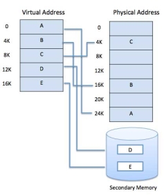
A computer can address more memory than the amount physically installed on the system. This extra memory is actually called virtual memory and it is a section of a hard disk that's set up to emulate the computer's RAM.
The main visible advantage of this scheme is that programs can be larger than physical memory. Virtual memory serves two purposes. First, it allows us to extend the use of physical memory by using disk. Second, it allows us to have memory protection, because each virtual address is translated to a physical address.
Following are the situations, when entire program is not required to be loaded fully in main memory.
- User written error handling routines are used only when an error occurred in the data or computation.
- Certain options and features of a program may be used rarely.
- Many tables are assigned a fixed amount of address space even though only a small amount of the table is actually used.
- The ability to execute a program that is only partially in memory would counter many benefits.
- Less number of I/O would be needed to load or swap each user program into memory.
- A program would no longer be constrained by the amount of physical memory that is available.
- Each user program could take less physical memory, more programs could be run the same time, with a corresponding increase in CPU utilization and throughput.
Modern microprocessors intended for general-purpose use, a memory management unit, or MMU, is built into the hardware. The MMU's job is to translate virtual addresses into physical addresses. A basic example is given below −
|
Fig 14 – Memory Address
Virtual memory is commonly implemented by demand paging. It can also be implemented in a segmentation system. Demand segmentation can also be used to provide virtual memory.
Demand Paging
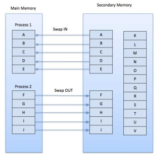
A demand paging system is quite similar to a paging system with swapping where processes reside in secondary memory and pages are loaded only on demand, not in advance. When a context switch occurs, the operating system does not copy any of the old program’s pages out to the disk or any of the new program’s pages into the main memory Instead, it just begins executing the new program after loading the first page and fetches that program’s pages as they are referenced.
|
Fig 15 – Swap in swap out
While executing a program, if the program references a page which is not available in the main memory because it was swapped out a little ago, the processor treats this invalid memory reference as a page fault and transfers control from the program to the operating system to demand the page back into the memory.
Following are the advantages of Demand Paging −
- Large virtual memory.
- More efficient use of memory.
- There is no limit on degree of multiprogramming.
- Number of tables and the amount of processor overhead for handling page interrupts are greater than in the case of the simple paged management techniques.
Page Replacement Algorithm
Page replacement algorithms are the techniques using which an Operating System decides which memory pages to swap out, write to disk when a page of memory needs to be allocated. Paging happens whenever a page fault occurs and a free page cannot be used for allocation purpose accounting to reason that pages are not available or the number of free pages is lower than required pages.
When the page that was selected for replacement and was paged out, is referenced again, it has to read in from disk, and this requires for I/O completion. This process determines the quality of the page replacement algorithm: the lesser the time waiting for page-ins, the better is the algorithm.
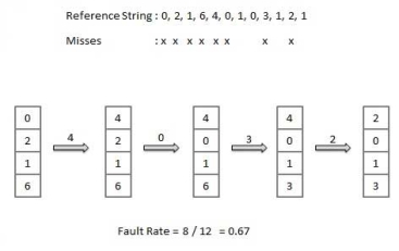
A page replacement algorithm looks at the limited information about accessing the pages provided by hardware, and tries to select which pages should be replaced to minimize the total number of page misses, while balancing it with the costs of primary storage and processor time of the algorithm itself. There are many different page replacement algorithms. We evaluate an algorithm by running it on a particular string of memory reference and computing the number of page faults,
Reference String
The string of memory references is called reference string. Reference strings are generated artificially or by tracing a given system and recording the address of each memory reference. The latter choice produces a large number of data, where we note two things.
- For a given page size, we need to consider only the page number, not the entire address.
- If we have a reference to a page p, then any immediately following references to page p will never cause a page fault. Page p will be in memory after the first reference; the immediately following references will not fault.
- For example, consider the following sequence of addresses − 123,215,600,1234,76,96
- If page size is 100, then the reference string is 1,2,6,12,0,0
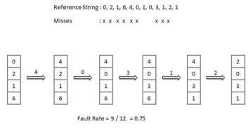
First In First Out (FIFO) algorithm
- Oldest page in main memory is the one which will be selected for replacement.
- Easy to implement, keep a list, replace pages from the tail and add new pages at the head.
|
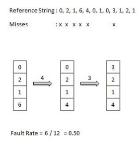
- An optimal page-replacement algorithm has the lowest page-fault rate of all algorithms. An optimal page-replacement algorithm exists, and has been called OPT or MIN.
- Replace the page that will not be used for the longest period of time. Use the time when a page is to be used.
|
Least Recently Used (LRU) algorithm
- Page which has not been used for the longest time in main memory is the one which will be selected for replacement.
- Easy to implement, keep a list, replace pages by looking back into time.
|
- To get a process start quickly, keep a pool of free frames.
- On page fault, select a page to be replaced.
- Write the new page in the frame of free pool, mark the page table and restart the process.
- Now write the dirty page out of disk and place the frame holding replaced page in free pool.
Least frequently Used (LFU) algorithm
- The page with the smallest count is the one which will be selected for replacement.
- This algorithm suffers from the situation in which a page is used heavily during the initial phase of a process, but then is never used again.
Most frequently Used (MFU) algorithm
- This algorithm is based on the argument that the page with the smallest count was probably just brought in and has yet to be used.
Key takeaways
- A computer can address more memory than the amount physically installed on the system. This extra memory is actually called virtual memory and it is a section of a hard disk that's set up to emulate the computer's RAM.
- The main visible advantage of this scheme is that programs can be larger than physical memory. Virtual memory serves two purposes. First, it allows us to extend the use of physical memory by using disk. Second, it allows us to have memory protection, because each virtual address is translated to a physical address.
The secondary storage devices which are built into the computer or connected to the computer are known as a secondary memory of the computer. It is also known as external memory or auxiliary storage.
The secondary memory is accessed indirectly via input/output operations. It is non-volatile, so permanently stores the data even when the computer is turned off or until this data is overwritten or deleted. The CPU can't directly access the secondary memory. First, the secondary memory data is transferred to primary memory then the CPU can access it.
Some of the secondary memory or storage devices are described below:
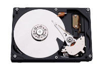
It is a rigid magnetic disc that is used to store data. It permanently stores data and is located within a drive unit.
|
Fig 16 – Hard disk
The hard disk is also known as a hard drive. It is a rigid magnetic disc that stores data permanently, as it is a non-volatile storage device. The hard disk is located within a drive unit on the computer's motherboard and comprises one or more platters packed in an air-sealed casing. The data is written on the platters by moving a magnetic head over the platters as they spin. The data stored on a computer's hard drive generally includes the operating system, installed software, and the user's files and programs, including pictures, music, videos, text documents, etc.
The main components of a hard drive include a head actuator, read/write actuator arm, read/write head, platter, and spindle. A circuit board, which is called the disk controller or interface board, is present on the back of a hard drive. It allows the hard drive to communicate with the computer.
|
Fig 17 - SSD
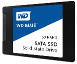
SSD (Solid State Drive) is also a non-volatile storage medium that is used to hold and access data. Unlike a hard drive, it does not have moving components, so it offers many advantages over SSD, such as faster access time, noiseless operation, less power consumption, and more.
As the cost of SSD has come down, it has become an ideal replacement for a standard hard drive in desktop and laptop computers. It is also suitable for notebooks, and tablets that don't require lots of storage.
|
Fig 18 – Pen drive
Pen drive is a compact secondary storage device. It is also known as a USB flash drive, thumb drive or a jump drive. It connects to a computer via a USB port. It is commonly used to store and transfer data between computers. For example, you can write a report using a computer and then copy or transfer it in the pen drive. Later, you can connect this pen drive to a computer to see or edit your report. You can also store your important documents and pictures, music, videos in the pen drive and keep it at a safe place.
Pen drive does not have movable parts; it comprises an integrated circuit memory chip that stores the data. This chip is housed inside a plastic or aluminium casing. The data storage capacity of the pen drive generally ranges from 2 GB to 128 GB. Furthermore, it is a plug and play device as you don't need additional drives, software, or hardware to use it.
|
Fig 19 – SD card
SD Card stands for Secure Digital Card. It is most often used in portable and mobile devices such as smartphones and digital cameras. You can remove it from your device and see the things stored in it using a computer with a card reader.
There are many memory chips inside the SD card that store the data; it does not have moving parts. SD cards are not created equal, so they may differ from each other in terms of speed, physical sizes, and capacity. For example, standard SD cards, mini-SD cards, and micro-SD cards.
|
Fig 20 - CD
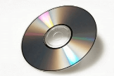
Compact Disk is a portable secondary storage device in the shape of a round medium disk. It is made of polycarbonate plastic. The concept of CD was co-developed by Philips and Sony in 1982. The first CD was created on 17 August 1982 at the workshop of Philips in Germany.
In the beginning, it was used for storing and playing sound recordings, later it was used for various purposes such as for storing documents, audio files, videos, and other data like software programs in a CD.
Physical characteristics of a CD/ Structure of CD:
A standard CD is around 5 inches in diameter and 0.05 inches in thickness. It is made of a clear polycarbonate plastic substrate, a reflective metallic layer, and a clear coating of acrylic plastic. These thin circular layers are attached one on top of another as described below:
- A polycarbonate disc layer at the bottom has the data encoded by creating lands and pits.
- The polycarbonate disc layer is coated with a thin aluminium layer that reflects the laser.
- The reflective aluminium layer is coated with a lacquer layer to prevent oxidation in order to protect the below layers. It is generally spin coated directly on the top of the reflective layer.
- The label print is applied on the lacquer layer, or artwork is screen printed on the top of the disc on the lacquer layer by offset printing or screen printing.
The data or information is stored or recorded or encoded in CD digitally using a laser beam that etches tiny indentations or bumps on its surface. The bump is called a pit, which represents the number 0. Space, where the bump is not created, is called land, and it represents the number 1. Thus, the data is encoded into a compact disc by creating pits (0) and lands (1). The CD players use laser technology to read the optically recorded data.
|
Fig 21 - DVD
DVD is short for digital versatile disc or digital video disc. It is a type of optical media used for storing optical data. Although it has the same size as a CD, its storage capacity is much more than a CD. So, it is widely used for storing and viewing movies and to distribute software programs as they are too large to fit on a CD. DVD was co-developed by Sony, Panasonic, Philips, and Toshiba in 1995.
DVDs can be divided into three main categories which are as follows:
- DVD-ROM (Read-Only): These types of DVDs come with media already recorded on them, such as movie dvds. As the name suggests, data on these discs cannot be erased or added, so these discs are known as a read-only or non-writable DVD.
- DVD-R (Writable): It allows you to record or write information to the DVD. However, you can write information only once as it becomes a read-only DVD once it is full.
- DVD-RW (Rewritable or Erasable): This type of discs can be erased, written, or recorded multiple times.
Key takeaways
- The secondary storage devices which are built into the computer or connected to the computer are known as a secondary memory of the computer. It is also known as external memory or auxiliary storage.
- The secondary memory is accessed indirectly via input/output operations. It is non-volatile, so permanently stores the data even when the computer is turned off or until this data is overwritten or deleted. The CPU can't directly access the secondary memory. First, the secondary memory data is transferred to primary memory then the CPU can access it.
References
1. William Stallings: Computer Organization & Architecture, 7th Edition, PHI, 2006.
2. Vincent P. Heuring & Harry F. Jordan: Computer Systems Design and Architecture, 2 nd Edition, Pearson Education, 2004.
