The microprocessor has become a more essential part of many gadgets. The evolution of microprocessor was divided into five generations such as first, second, third, fourth, and fifth-generation and the characteristics of these generations are discussed below.
First Generation Microprocessors
The first generation microprocessors were introduced in the year 1971-1972. The instructions of these microprocessors were processed serially, they fetched the instruction, decoded and then executed it. When an instruction of the microprocessor was finished, then the microprocessor updates the instruction pointer & fetched the following instruction, performing this consecutive operation for each instruction in turn.
Second Generation Microprocessors
In the year 1970, a small number of transistors were available on the integrated circuit in the second-generation microprocessors. Examples of the second-generation microprocessors are 16-bit arithmetic 7 pipelined instruction processing, MC68000 Motorola microprocessor. The second generation of the microprocessor is defined by overlapped fetch, decode, and execute the steps. When the first generation is processed in the execution unit, then the second instruction is decoded and the third instruction is fetched.
Third Generation Microprocessors
The third-generation microprocessors were introduced in the year 1978, as denoted by Intel’s 8086 and the Zilog Z8000. These were 16-bit processors with a performance like mini computers. These types of microprocessors were different from the previous generations of microprocessors in that all main workstation industrialists began evolving their own ISC based microprocessor architectures.
Fourth Generation Microprocessors
As many industries converted from commercial microprocessors to in house designs, the fourth-generation microprocessors are entered with outstanding design with a million transistors. Leading-edge microprocessors like Motorola’s 88100 and Intel’s 80960CA could issue & retire more than one instruction per clock cycle.
Fifth Generation Microprocessors
Fifth-generation microprocessors employed decoupled superscalar processing, and their design soon exceeded 10 million transistors. In the fifth generation, PCs are a low-margin, high volume business conquered by a single microprocessor.
Key takeaways
The microprocessor is clock driven sequential device. There are 8-bit, 16-bits, 64-bits of microprocessors.
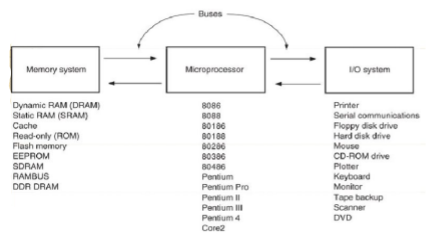
The introduction of microprocessors had a huge impact in the way we use computers. Computers that once took large areas were reduced to the size of small desktops. Although these desktop computers are small and compact, they possess computing power more than that of the large size computers of the previous generation. Here, in this section, we are going to learn about the structure of a microprocessor based personal computer system. The block diagram of a personal computer system is shown in the figure. This block diagram also applies to any computer system, from the early mainframe computers to the modern microprocessor-based systems. The block diagram is shown below.
|
Fig 1 Block Diagram of Microprocessor Based System
The memory and the input/output system
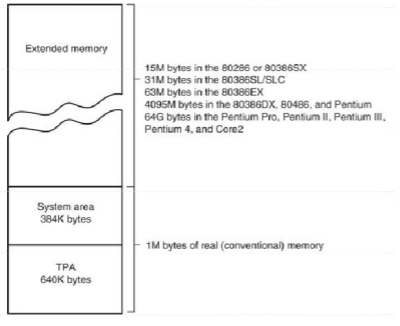
The memory structure of all Intel 80x86 to Pentium 4 based personal computer systems are similar. This includes the first computers based on 8088 introduced in 1981 by IBM to the most modern computers based on Pentium 4. The memory structure of microprocessor-based computer systems can be divided into three main regions. These are
Transient program area (TPA)
System area
Extended memory system (XMS)
|
Fig 2 Memory Map
It should be noted that the Extended memory system is not available in those computers based on 8086 or 8088. In these old computers the TPA and System area exists but not the Extended memory system. The TPA is of size 640 Kb and System area is of size 384Kb. The TPA and System area together forms the real or conventional memory which is of size 1024Kb or 1 Mb. It's called as real or conventional memory because each Intel microprocessor is designed to function in this area using its real mode of operation.
Those computer systems that uses the any of the microprocessors, Intel 80286 through Pentium 4, has the 640 Kb of TPA and 384 Kb of system area, In addition , these systems also have an Extended memory. Hence IBM designates these systems as AT class machines (AT- Advanced class computer systems). These systems are also called as ISA (Industry standard architecture) or EISA (Extended ISA). The extended memory available in the computer systems using the 80286- 80386SX microprocessors is 15Mb. While the amount of extended memory available in the computer systems using 80386DX - Pentium microprocessors are 4095Mb, excluding the 1Mb real or conventional memory. The Computer systems having Pentium pro - Pentium 4 microprocessors can have 1Mb less than 4Gb to 64GB extended memory.
The Transient Program area (TPA)
The transient program area or TPA holds the DOS operating system and other programs that control the computer system. The TPA also holds other active or inactive application programs. We know that the TPA is 640Kb and since it holds DOS on it a part of this 640 kb is used up by DOS operating system. The size of the TPA available for other application programs is 628Kb if MS-DOS version 7.X is used as the operating system. The older versions of DOS used to take up large spaces of TPA leaving only less than 530Kb for other applications. PCDOS is another operating system that is found in computer systems. Both PC-DOS and MSDOS are compatible with each other, hence both functioned similarly with application programs. Windows and OS/2 are other operating systems compatible with DOS and allows DOS programs to execute.
|
Fig 3 Memory Map of TPA
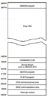
The memory map of the TPA is shown in the figure. The memory map shows how different areas of the TPA are allotted to the system programs, data and drivers. To the left of each area is a hexadecimal number that shows the memory address that begin and end each data area.
Interrupt Vectors - The interrupt vectors which occupy the area between 00000 and 00400 is responsible for accessing various features of the DOS, BIOS and other application programs.
BIOS communication area and DOS communication area - BIOS is nothing but Basic Input/Output System. BIOS is a collection of programs that is stored in the ROM or flash memory that is used to control the Input/Output devices that is connected to the computer system. The BIOS and DOS communication areas have transient data that can be used by programs to access the I/O devices or other parts of the computer system.
IO.SYS - The IO.SYS is a program that loads into the TPA from the disk when the computer system using MSDOS or PCDOS are switched ON. The programs in the IO.SYS enables the DOS programs to use the keyboard, the display, printer and other I/O devices.
MSDOS - MSDOS occupies two parts of the TPA. One is at the top of TPA which is considerably small and 16 bytes in length. The other is at the bottom and is larger. The memory size occupied by the DOS depends on the version of the DOS installed. Older versions usually needed larger areas of TPA compared to the newer versions.
Device Drivers- Drivers are those files with an extension .SYS such as MOUSE.SYS. Drivers are programs that control the installable devices like mouse, hand scanner and also other installable application programs. The size of the driver and the number of drivers vary from one computer to the another.
COMMAND.COM- The COMMAND.COM helps to control the computer system using the keyboard when operated in DOS mode. The COMMAND.COM program processes the DOS commands as they are typed from the keyboard.
Free TPA- The free TPA holds the active DOS application programs. These DOS application programs can be exemplified as the word processor, spreadsheet and CAD programs. In addition to these, free TPA also holds the TSR (Terminate and Stay Resident) programs. These remain in the free TPA in an inactive state until initiated by a hot-key or an interrupt. hotkey. An example of TSR is the calculator program that is activated upon the ALT+C.
SYSTEM AREA
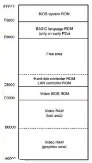
The System area which is smaller than the TPA is considerably important. It contains programs for data storage and these programs are stored in ROM or flash memory and also in some areas of the RAM. The system area map is shown in the figure.
|
Fig 4 System Area
On the left side memory addresses of the particular regions are given in hexadecimal format. The first area of the system space extends from A0000H to C7FFFH and has the video display RAM and video control programs. The Video display RAM is stored in two parts, first from A0000H to A7FFFH and is for the graphical data, second from B0000H to B7FFFH and stores the text data. The video BIOS contains programs that control the video display of the computer and is located on ROM or flash memory. It's area in system space is from C0000H to C7FFFH. The size and amount of the memory used depends upon the type of video display adapter used.
The area C8000H - DFFFFH is free system area and is called the open system area. It is mostly used as the extended memory system in PC and XT machines (PC and XT machines means those computers based on 8086/8088 microprocessor) and as an upper memory system in AT class machines (Computers using 80286 or above microprocessors). Memory locations E0000H-EFFFFH contains the cassette BASIC language on ROM found in the older IBM based systems. In almost all the newer systems this particular area is kept open or free and is also used as RAM to aid the faster operation of DOS application programs.
The system area F0000H to FFFFFH is used by the System BIOS ROM, but this System BIOS ROM only operates the I/O devices and is not responsible for the controlling of the video display system which is done by the separate system BIOS ROM at the location C0000H. The system BIOS at the top is divided into two parts, first part is in the area F0000H to F7FFFH and contains programs that set up the computer. The second part contains procedures that control the I/O devices.
Key takeaway
It should be noted that the Extended memory system is not available in those computers based on 8086 or 8088. In these old computers the TPA and System area exists but not the Extended memory system. The TPA is of size 640 Kb and System area is of size 384Kb.
The interrupt vectors which occupy the area between 00000 and 00400 is responsible for accessing various features of the DOS, BIOS and other application programs.
Operations of 8085 Microprocessor
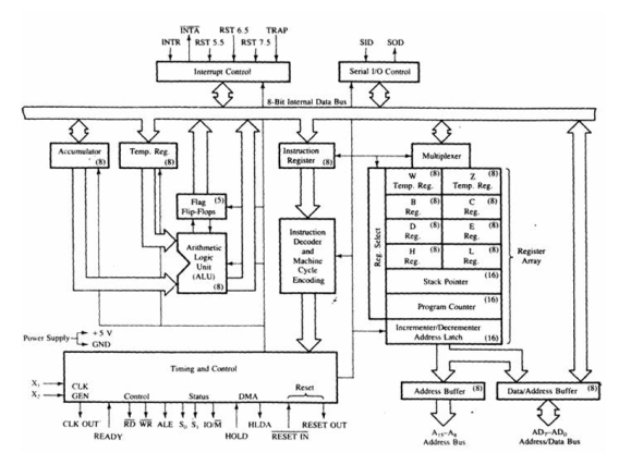
It performs all arithmetical and logical operations like add, subtract, AND, OR etc. The temporary registers and accumulators hold the information throughout the operations and the result is stored in the accumulator. The different flags are arranged or rearranged on the basis of result.
Flag Registers
It is an 8 bit register. They are of five types namely sign, zero, auxiliary carry, parity and carry.
Control and Timing Unit
It coordinates with all the processes of the microprocessor by the clock and provides the control signals required for communication between the microprocessor and peripherals. It is used to control the internal as well as external circuits.
- Decoder and Instruction Register
when an order is received from memory which is located in the instruction register, it is encoded & decoded into various device cycles.
Register Array
The general purpose registers are classified into several types such as B, C, D, E, H, & L. They are 8-bit registers. The register pairs are BC, DE & HL.
- Special Purpose Registers
These registers are of four types namely program counter, stack pointer, increment or decrement register, address or data buffer.
Program Counter
It is a 16 bit register. It is used to store data, memory information etc. whenever memory is incremented, the PC then points to the next location.
Stack Pointer
It is a 16 bit register. It always points to stack which can be incremented or decremented by PUSH and POP instruction.
Increment or Decrement Register
It is an 8-bit register which can be increased or decreased by one. It is useful for incrementing or decrementing program counters as well as stack pointer register content with one. This operation can be done on any memory location or any kind of register.
Address Bus and Data Bus
Data bus carries the data required to be stored. It is bidirectional. Address bus carries the location to where the data should be stored and it is unidirectional. It is used to transfer the data & address.
|
Fig.5: Architecture of 8085 (ref 1)
Key takeaway
It includes the timing & control unit, Arithmetic and logic unit, decoder, instruction register, interrupt control, a register array, serial input/output control and the central processing unit.
Two Real modes of addressing on 80x86 Pentium 4 comes up in the real-mode after it is reset. It will remain in this mode unless it is switched to protected-mode by software.
• In real mode, the Pentium 4 operates as a very high performance 8086.
• Pentium 4 can be used to execute the base instruction set of the 8086 MPU.
In addition, a number of new instructions (called extended instruction set) have been added to enhance its performance and functionality (such new instructions can be run in the real-mode as well as the protected-mode). In real-mode, only the first 1 M bytes of memory can be addressed with the typical segment off-set logical address. Each segment is 64K bytes long. Pentium 4 microprocessor has 36-bit address bus, which means it can support up to 236 = 64G bytes of total memory.
Real mode flat model means strictly converting one address value into a physically meaningful location in the RAM. Real mode segmented model means o location. strictly converting two address values into a physically meaningful memory o gives access to one megabyte (1,048,576 bytes) of directly addressable memory, known as real mode memory.
Segment Registers
Segment registers are basically memory pointers located inside the CPU.
Segment registers point to a place in memory where one of the following things begin:
- Data storage
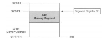
- Code execution. Example: code segment register CS points to a 64K region of memory:
|
Fig 6 Code Segment Register
Real Mode Segmented Model
• Segmented organization o 16-bit wide segments
• Two components: Base (16 bits) and Offset (16 bits)
• Two-component specification is called logical address, also called effective address.
• Logical address translates to a 20-bit physical address.
• Addresses are limited to 20 bits: 2 20=1,048,576 bytes.
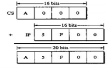
• Physical address is generated by adding a 16-bit segment register, shifted left four plus a 16 bit-offset.
• Generating 20-bit physical address in Real Mode
|
Fig 7 Physical address in real mode
Problems Related to Segmentation
• Segmentation structures: often caused grief for programmers who tried to access large data o Since an offset cannot exceed 16 bits, you cannot increment beyond 64k.
• Instead, program must watch out for a 64k boundary and then play games with the segment register.
• This nightmare was originally created to support CP/M-80 programs ported from 8080 chip to 8086.
Address Space in Real Mode
• Address space in real mode segmented model runs from o 00000h to 0FFFFFh, within one megabyte of memory.
• For compatibility reasons, Pentium CPU is capable of switching itself into real mode segmented model, is effectively becoming a good old 8086 chip.
Key takeaway
Two Real modes of addressing on 80x86 Pentium 4 comes up in the real-mode after it is reset. It will remain in this mode unless it is switched to protected-mode by software.
Reference:
1. Gaonkar, Ramesh S , “Microprocessor Architecture, Programming and Applications with 8085”, Penram International Publishing.
2. Ray A K, Bhurchandi K M, “Advanced Microprocessors and Peripherals”, TMH Hall D V, Microprocessor Interfacing’, TMH
3.Liu and, “Introduction to Microprocessor”, TMH
4. Brey, Barry B, “INTEL Microprocessors”, PHI
