UNIT - 6
Hardware Specifications, Memory Interface – 1
|
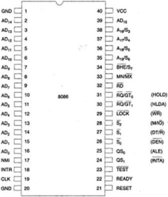
Fig 1: Pin Diagram
- It uses 5V DC supply at VCC pin 40, and uses ground at VSS pin 1 and 20 for its operation.
- Clock signal is provided at Pin-19. It is used to provide timing to the processor for operations. Its frequency varies for different versions, i.e. 5MHz, 8MHz and 10MHz.
- AD0-AD15 are 16 address/data bus. AD0-AD7 carries lower order data byte and AD8-AD15 carries higher order data byte.
- A16-A19/S3-S6 are the 4 address/status buses. During the first clock cycle, they carry 4-bit address and then carries status signals.
- BHE stands for Bus High Enable. It is present at pin 34 and used to indicate the transfer of data using data bus D8-D15. This is low signal present during the first clock cycle and thereafter it is active.
- RD is present at pin 32 and is used for Read operation.
- READY is available at pin 22. It is an active high signal. It is an acknowledgement signal from I/O devices when data is transferred. When it is high, it indicates that the device is ready to transfer data else it indicates wait state.
- RESET is available at pin 21 and is used for restarting the execution. The processor immediately terminates its present activity when it is executed. This signal is active high for the first 4 clock cycles to RESET the microprocessor.
- INTR is at pin 18. It is an interrupt request signal which is used to determine if the processor has an interrupt or not.
- NMI stands for non-maskable interrupt and is at pin 17. It is an edge triggered input which causes an interrupt request to the microprocessor.
- TEST signal is same as wait state and is present at pin 23. When it is high, then the processor has to wait for IDLE state else the execution continues.
- MN/MX stands for Minimum/Maximum and is present at pin 33. It shows what mode the processor is operating in. When it is high, it works in the minimum mode and vice-a-versa.
- INTA is an interrupt acknowledgement signal and is present at pin 24. When the microprocessor receives this signal, it acknowledges the interrupt.
- ALE stands for address latch enable and is available at pin 25. A positive pulse is generated each time the processor begins any operation. This signal indicates the availability of address on the address/data lines.
- DE stands for Data Enable and is available at pin 26. It is used to enable Transreceiver 8286.
- DT/R stands for Data Transmit/Receive signal and is present at pin 27. It decides the direction of data flow with the help of the transreceiver. When it is high, data is transmitted and vice-a-versa.
- M/IO is used to distinguish between memory and I/O operations. When it is high, it indicates I/O operation and when low it indicates the memory operation. It is present at pin 28.
- WR stands for write signal and is present at pin 29. It is used for writing the data into the memory or the output device depending on the status of M/IO signal.
- HLDA stands for Hold Acknowledgement signal and is present at pin 30. This signal acknowledges the HOLD signal.
- HOLD indicates the processor that external devices are requesting to access its address/data buses. It is present at pin 31.
- The queue status signals are present at pin 24 and 25. They provide the status of instruction queue and their conditions are–
QS0 | QS1 | Status |
0 | 0 | No operation |
0 | 1 | First byte of opcode from the queue |
1 | 0 | Empty the queue |
1 | 1 | Subsequent byte from the queue |
- S0, S1, S2
They are the status signals that provides the status of operation used by the Bus Controller 8288 to generate memory & I/O control signals. These are present at pin 26, 27, and 28.
S2 | S1 | S0 | Status |
0 | 0 | 0 | Interrupt acknowledgement |
0 | 0 | 1 | I/O Read |
0 | 1 | 0 | I/O Write |
0 | 1 | 1 | Halt |
1 | 0 | 0 | Opcode fetch |
1 | 0 | 1 | Memory read |
1 | 1 | 0 | Memory write |
1 | 1 | 1 | Passive |
- When LOCK is active, it shows to the other processors not to request the CPU to leave the system bus. It is present at pin 29.
- RQ/GT1 and RQ/GT0 are the Request/Grant signals used by the other processors to request the CPU to free the system bus. When the signal is received by CPU, it sends acknowledgment. RQ/GT0 has a higher priority than RQ/GT1.
Key takeaway
It is a 40-pin chip. AD0-AD15 are 16 address/data bus. AD0-AD7 carries lower order data byte and AD8-AD15 carries higher order data byte.
A16-A19/S3-S6 are the 4 address/status buses. During the first clock cycle, they carry 4-bit address and then carries status signals.
|
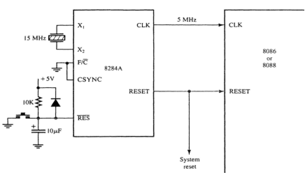
Fig 2 Clock Generator
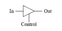
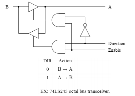
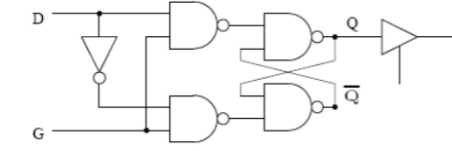
Latches are used to de-multiplex the address/data and address/status lines and commonly have output buffers for driving external loads. Buffers are used to drive external loads, and to isolate component when disabled.
|
Fig 3 Latches for various purpose
When enabled by the control line, output follows input (buffered, pass-through). When disabled, output is a very high impedance which prevents the output from driving or loading connected circuits. When disabled, the outputs are said to be floating. It is like a switch.
|
Fig 4 Latches
When enable is high, Q follows D. • When enable goes low, Q maintains (latches) state of D.
Key takeaway
Latches are used to de-multiplex the address/data and address/status lines and commonly have output buffers for driving external loads. Buffers are used to drive external loads, and to isolate component when disabled.
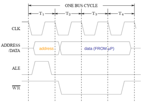
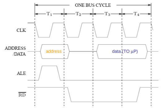
8086 and 8088 bus cycles consume four system clock periods (T-states), T1, T2, T3 and T4. At 5MHz, each T-state is 200nS, therefore a bus cycle is 800nS. Semi-synchronous bus control allows inserting of wait states (Tw), also 200nS, between T3 and T4 which allows access to slow memory and I/O devices. Most processors are very similar in I/O and memory access operations.
|
Fig 5 Write Cycle
|
Fig 6 Read Cycle
T1: Address, ALE, DT/R, M/IO.
T2: RD, WR, DEN, data on the bus (for write).
At the end of T2 (middle of T3), µP samples READY
T3 /Tw: Gives time for memory or I/O device to read/write.
For read cycles, data bus is sampled at end of T3.
T4: All bus signals are deactivated.
Key takeaway
Normal memory access time is 460nS. Slower devices will need at least one wait state which will give 660nS.
Wait state (TW): It is an extra clocking period, inserted between T2 & T3 in order to give memory and other slow devices to complete data transfer.
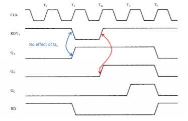
READY input: This input causes wait states for slower memory & I/O components. It is sampled at the end of T2, and if applicable, in middle of TW. If READY = 0 at end of T2: T3 is delayed and TW is inserted between T2 and T3. READY is next sampled at middle of TW: to determine whether the next state is another TW or T3.
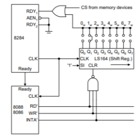
The timing requirements of the Ready signal are given below. These requirements are guaranteed by the 8284A clock generator. 8284A receives wait state information via its RDY input and then through its internal synchronization circuitry, it generates Ready signal for microprocessor. If one wait state in inserted, then the memory access time, normally 460 ns with a 5 MHz clock, is lengthened by one clocking period (200ns) to 660 ns
|
Fig 7 Time Required for Ready Signal
Wait State Generation Circuit
|
Fig 8 Wait State Generation Circuit
|
Fig 9 Wait State Generation Timing Diagram
Key takeaway
Wait state (TW): It is an extra clocking period, inserted between T2 & T3 in order to give memory and other slow devices to complete data transfer.
READY input: This input causes wait states for slower memory & I/O components.
8086 microprocessor operates in 2 modes:
Minimum mode
- It can be selected by setting MN/MX pin to logic 1 and it acts like a single microprocessor.
- In this mode, all the control signals are provided by the microprocessor chip itself.
Maximum mode
- This operation can be selected by setting MN/MX pin to logic 0 and microprocessor acts like a multiprocessor.
- It provides the signals for implementing a multi core processor system environment and in this each processor executes its own program.
- In this type of system environment, some system resources that are common to all processors are present.
- They are known as global resources.
- Co-processor means there is a second processor in the system, but both of them cannot access the system bus at the same time.
One processor passes the control of the system bus to the other & then can also suspend its operation.
Key takeaway
8086 microprocessor operates in 2 modes:
Minimum mode: It can be selected by setting MN/MX pin to logic 1 and it acts like a single microprocessor.
Maximum mode: This operation can be selected by setting MN/MX pin to logic 0 and microprocessor acts like a multiprocessor.
When we are executing any instruction, we need the microprocessor to access the memory for reading instruction codes and the data stored in the memory. For this, both the memory and the microprocessor require some signals to read from and write to registers.
The interfacing process includes some key factors to match with the memory requirements and microprocessor signals. The interfacing circuit therefore should be designed in such a way that it matches the memory signal requirements with the signals of the microprocessor.
Reference:
1. Gaonkar, Ramesh S , “Microprocessor Architecture, Programming and Applications with 8085”, Penram International Publishing.
2. Ray A K, Bhurchandi K M, “Advanced Microprocessors and Peripherals”, TMH Hall D V, Microprocessor Interfacing’, TMH
3.Liu and, “Introduction to Microprocessor”, TMH
4. Brey, Barry B, “INTEL Microprocessors”, PHI
